


When a data register is used as either a source or a destination operand, only the appropriate low-order portion is changed; the remaining high-order portion is neither used nor changed.
2.3.2 Address Registers
Each address register (and the stack pointer) is 32 bits wide and holds a full, 32-bit address. Address registers do not support byte-sized operands. Therefore, when an address register is used as a source operand, either the low-order word or the entire long-word operand is used, depending upon the operation size. When an address register is used as the destination operand, the entire register is affected, regardless of the operation size. If the operation size is word, operands are sign-extended to 32 bits before the operation is performed.
2.4 DATA ORGANIZATION IN MEMORY
Bytes are individually addressable. As shown in Figure 2-5, the high-order byte of a word has the same address as the word. The low-order byte has an odd address, one count higher. Instructions and multibyte data are accessed only on word (even byte) boundaries. If a long-word operand is located at address n (n even), then the second word of that operand is located at address n+2.
15 |
14 |
13 |
12 |
11 |
10 |
9 |
8 |
|
7 |
6 |
5 |
4 |
3 |
2 |
1 |
0 |
|
||
ADDRESS |
|
|
|
|
|
|
|
|
WORD 0 |
|
|
|
|
|
|
|
|
|
|
$000000 |
|
|
|
|
BYTE 000000 |
|
|
|
|
|
|
|
BYTE 000001 |
|
|
|
|
||
|
|
|
|
|
|
|
|
|
|
|
|
|
|
|
|
|
|
|
|
$000002 |
|
|
|
|
BYTE 000002 |
|
|
WORD 1 |
|
|
|
|
|
|
|
|
|
||
|
|
|
|
|
|
|
|
|
|
|
BYTE 000003 |
|
|
|
|
||||
|
|
|
|
|
|
|
|
|
|
|
|
|
|
|
|
||||
|
|
|
|
|
|
|
|
|
|
|
|
|
|
|
|
|
|
|
|
|
|
|
|
|
|
|
|
|
|
|
|
|
|
|
|
|
|
|
|
|
|
|
|
|
|
$FFFFFE |
|
WORD 7FFFFF |
|||
BYTE FFFFFE |
|
BYTE FFFFFE |
|||
|
|
|
|||
|
|
|
|
|
|
Figure 2-5. Word Organization in Memory
The data types supported by the M68000 MPUs are bit data, integer data of 8, 16, and 32 bits, 32-bit addresses, and binary-coded-decimal data. Each data type is stored in memory as shown in Figure 2-6. The numbers indicate the order of accessing the data from the processor. For the MC68008 with its 8-bit bus, the appearance of data in memory is identical to the all the M68000 MPUs. The organization of data in the memory of the MC68008 is shown in Figure 2-7.
2-6 |
M68000 8-/16-/32-BIT MICROPROCESSOR USER’S MANUAL |
MOTOROLA |
|
|
|
|
|
|
|
|
|
BIT DATA |
|
|
|
|
|
|
|
|||
|
|
|
|
|
|
|
|
1 BYTE = 8 BITS |
|
|
|
|
|
|
|
||||
|
|
|
|
|
7 |
6 |
5 |
4 |
|
3 |
|
2 |
1 |
0 |
|
|
|
|
|
|
|
|
|
|
|
|
|
|
|
|
|
|
|
|
|
|
|
|
|
|
|
|
|
|
|
|
|
INTEGER DATA |
|
|
|
|
|
|
|
||||
|
|
|
|
|
|
|
|
1 BYTE = 8 BITS |
|
|
|
|
|
|
|
||||
15 |
14 |
13 |
12 |
|
11 |
10 |
9 |
8 |
|
7 |
|
6 |
5 |
4 |
3 |
2 |
1 |
0 |
|
MSB |
|
|
BYTE 0 |
|
|
|
LSB |
|
|
|
|
BYTE 1 |
|
|
|
||||
|
|
|
|
|
|
|
|
|
|
|
|
|
|
|
|
|
|||
|
|
|
BYTE 2 |
|
|
|
|
|
|
|
|
|
BYTE 3 |
|
|
|
|||
|
|
|
|
|
|
|
|
|
|
|
|
|
|
|
|
|
|
|
|
|
|
|
|
|
|
|
1 WORD = 16 BITS |
|
|
|
|
|
|
|
|||||
15 |
14 |
13 |
12 |
|
11 |
10 |
9 |
8 |
|
7 |
|
6 |
5 |
4 |
3 |
2 |
1 |
0 |
|
MSB |
|
|
|
|
|
|
|
|
WORD 0 |
|
|
|
|
|
|
LSB |
|||
|
|
|
|
|
|
|
|
|
|
|
|
|
|
|
|
|
|
||
|
|
|
|
|
|
|
|
|
WORD 1 |
|
|
|
|
|
|
|
|||
|
|
|
|
|
|
|
|
|
|
|
|
|
|
|
|
|
|||
|
|
|
|
|
|
|
|
|
WORD 2 |
|
|
|
|
|
|
|
|||
|
|
|
|
|
|
|
|
|
|
|
|
|
|
|
|
|
|||
|
|
EVEN BYTE |
|
|
|
|
|
|
|
|
|
|
ODD BYTE |
|
|
|
|||
7 |
6 |
5 |
4 |
|
3 |
2 |
1 |
0 |
|
7 |
|
6 |
5 |
4 |
3 |
2 |
1 |
0 |
|
|
|
|
|
|
|
|
1 LONG WORD = 32 BITS |
|
|
|
|
|
|
||||||
15 |
14 |
13 |
12 |
|
11 |
10 |
9 |
8 |
|
7 |
|
6 |
5 |
4 |
3 |
2 |
1 |
0 |
|
MSB |
|
|
|
|
|
|
|
|
HIGH ORDER |
|
|
|
|
|
|
|
|||
|
|
LONG WORD 0 |
|
|
|
|
|
|
|
|
|
|
|||||||
|
|
|
|
|
|
|
|
|
|
|
|
|
|
|
|
||||
|
|
|
|
|
|
|
|
|
LOW ORDER |
|
|
|
|
|
|
LSB |
|||
|
|
LONG WORD 1 |
|
|
|
|
|
|
|
|
|
|
|
|
|
|
|
||
|
|
|
|
|
|
|
|
|
|
|
|
|
|
|
|
|
|
||
|
|
LONG WORD 2 |
|
|
|
|
|
|
|
|
|
|
|
|
|
|
|
||
|
|
|
|
|
|
|
|
|
|
|
|
|
|
|
|
|
|||
|
|
|
|
|
|
|
|
|
ADDRESSES |
|
|
|
|
|
|
|
|||
|
|
|
|
|
|
|
1 ADDRESS = 32 BITS |
|
|
|
|
|
|
||||||
15 |
14 |
13 |
12 |
|
11 |
10 |
9 |
8 |
|
7 |
|
6 |
5 |
4 |
3 |
2 |
1 |
0 |
|
MSB |
|
|
|
|
|
|
|
|
HIGH ORDER |
|
|
|
|
|
|
|
|||
|
|
ADDRESS 0 |
|
|
|
|
|
|
|
|
|
|
|
||||||
|
|
|
|
|
|
LOW ORDER |
|
|
|
|
|
|
|
||||||
|
|
|
|
|
|
|
|
|
|
|
|
|
|
|
LSB |
||||
ADDRESS 1
ADDRESS 2
MSB = MOST SIGNIFICANT BIT
LSB = LEAST SIGNIFICANT BIT
|
|
|
|
|
|
|
DECIMAL DATA |
|
|
|
|
|
|
|
|
|
|
|
|
2 BINARY-CODED-DECIMAL DIGITS = 1 BYTE |
|
|
|
|
|
||||||
15 |
14 |
13 |
12 |
11 |
10 |
9 |
8 |
7 |
6 |
5 |
4 |
3 |
2 |
1 |
0 |
MSD |
|
BCD 0 |
|
|
|
BCD 1 |
|
|
BCD 2 |
|
|
|
BCD 3 |
|
|
|
|
|
|
|
LSD |
|
|
|
|
|
|
||||
|
|
|
|
|
|
|
|
|
|
|
|
|
|
|
|
|
|
BCD 4 |
|
|
|
BCD 5 |
|
|
BCD 6 |
|
|
|
BCD 7 |
|
|
|
|
|
|
|
|
|
|
|
|
|
|
|
|
|
|
MSD = MOST SIGNIFICANT DIGIT
LSD = LEAST SIGNIFICANT DIGIT
Figure 2-6. Data Organization in Memory
MOTOROLA |
M68000 8-/16-/32-BIT MICROPROCESSOR USER’S MANUAL |
2-7 |

|
|
BIT DATA 1 BYTE = 8 BITS |
|
|
||||
7 |
6 |
5 |
4 |
3 |
2 |
|
1 |
0 |
|
|
|
|
|
|
|
|
|
|
|
INTEGER DATA 1 BYTE = 8 BITS |
|
|||||||
7 |
6 |
5 |
4 |
3 |
2 |
1 |
|
|
0 |
|
|
|
|
BYTE 0 |
|
|
|
|
|
|
|
|
|
|
|
|
|
|
|
|
|
|
|
|
|
BYTE 1 |
|
|
|
|
|
|
|
|
|
|
|
|
|
|
|
|
|
|
|
|
|
BYTE 2 |
|
|
|
|
|
|
|
|
|
|
|
|
|
|
|
|
|
|
|
|
|
BYTE 3 |
|
|
|
|
|
|
|
|
|
|
|
|
|
|
||||
|
|
1 WORD = 2 BYTES = 16 BITS |
|
|||||||
BYTE 0 |
(MS BYTE) |
|
|
|
|
|
|
|
|
|
|
|
|
|
|
|
WORD 0 |
|
|
||
BYTE 1 |
(LS BYTE) |
|
|
|
|
|
||||
|
|
|
|
|
|
|
|
|||
|
|
|
|
|
|
|
|
|
||
BYTE 0 (MS BYTE) |
|
|
|
|
|
|
|
|
||
|
|
|
|
|
|
WORD 1 |
|
|
||
BYTE 1 |
(LS BYTE) |
|
|
|
|
|
||||
|
|
|
|
|
|
|
|
|||
|
|
|
|
|||||||
1 LONG WORD = 2 WORDS = 4 BYTES = 32 BITS |
||||||||||
BYTE 0 |
|
|
|
HIGH-ORDER |
|
|||||
|
|
|
|
|
|
|||||
BYTE 1 |
|
|
|
|
|
WORD |
|
|||
|
|
|
|
|
|
|
|
|
||
BYTE 2 |
LONG WORD 0 |
|
LOW-ORDER |
|
||||||
|
|
|
|
|
||||||
|
|
|
|
|
|
|
||||
BYTE 3 |
|
|
|
|
|
WORD |
|
|||
|
|
|
|
|
|
|
|
|
||
|
|
|
|
|
|
|
|
|
|
|
BYTE 0 |
|
|
|
HIGH-ORDER |
|
|||||
|
|
|
|
|
|
|||||
BYTE 1 |
|
|
|
|
|
WORD |
|
|||
|
|
|
|
|
|
|
|
|
||
BYTE 2 |
LONG WORD 1 |
|
LOW-ORDER |
|
||||||
|
|
|
|
|
||||||
|
|
|
|
|
|
|
||||
BYTE 3 |
|
|
|
|
|
WORD |
|
|||
|
|
|
|
|
|
|
|
|
||
|
|
|
|
|
|
|
|
|
|
|
LOWER ADDRESSES
HIGHER ADDRESSES
LOWER ADDRESSES
HIGHER ADDRESSES
LOWER ADDRESSES
HIGHER ADDRESSES
Figure 2-7. Memory Data Organization of the MC68008
2.5 INSTRUCTION SET SUMMARY
Table 2-2 provides an alphabetized listing of the M68000 instruction set listed by opcode, operation, and syntax. In the syntax descriptions, the left operand is the source operand, and the right operand is the destination operand. The following list contains the notations used in Table 2-2.
2-8 |
M68000 8-/16-/32-BIT MICROPROCESSOR USER’S MANUAL |
MOTOROLA |
Notation for operands:
PC — |
Program counter |
SR — |
Status register |
V — |
Overflow condition code |
Immediate Data — Immediate data from the instruction |
|
Source — |
Source contents |
Destination — Destination contents |
|
Vector — |
Location of exception vector |
+inf — |
Positive infinity |
–inf — |
Negative infinity |
<fmt> — |
Operand data format: byte (B), word (W), long (L), single |
|
(S), double (D), extended (X), or packed (P). |
FPm — |
One of eight floating-point data registers (always |
|
specifies the source register) |
FPn — One of eight floating-point data registers (always specifies the destination register)
Notation for subfields and qualifiers:
<bit> of <operand> — Selects a single bit of the operand <ea>{offset:width} — Selects a bit field
(<operand>) — The contents of the referenced location
<operand>10 — The operand is bina ry-coded decimal, operations are performed in decimal
(<address register>) — The register indirect operator
–(<address register>) — Indicates that the operand register points to the memory (<address register>)+ — Location of the instruction operand—the optional mode
qualifiers are –, +, (d), and (d, ix)
#xxx or #<data> — Immediate data that follows the instruction word(s)
Notations for operations that have two operands, written <operand> <op> <operand>, where <op> is one of the following:
→— The source operand is moved to the destination operand
↔— The two operands are exchanged
+— The operands are added
– — The destination operand is subtracted from the source operand
× — The operands are multiplied
÷ — The source operand is divided by the destination operand
< — Relational test, true if source operand is less than destination operand
> — Relational test, true if source operand is greater than destination operand
V — Logical OR
— Logical exclusive OR
Λ— Logical AND
MOTOROLA |
M68000 8-/16-/32-BIT MICROPROCESSOR USER’S MANUAL |
2-9 |
shifted by, rotated by — The source operand is shifted or rotated by the number of positions specified by the second operand
Notation for single-operand operations:
~<operand> — The operand is logically complemented
<operand>sign-extended — The operand is sign-extended, all bits of the upper portion are made equal to the high-order bit of the lower portion
<operand>tested — The operand is compared to zero and the condition codes are set appropriately
Notation for other operations:
TRAP — Equivalent to Format/Offset Word → (SSP); SSP–2 → SSP; PC → (SSP); SSP–4 → SSP; SR → (SSP); SSP–2 → SSP; (vector) → PC
STOP — Enter the stopped state, waiting for interrupts
If <condition> then — The condition is tested. If true, the operations after "then"
<operations> else |
are performed. If the condition is false and the optional |
<operations> |
"else" clause is present, the operations after "else" are |
|
performed. If the condition is false and else is omitted, the |
|
instruction performs no operation. Refer to the Bcc |
|
instruction description as an example. |
2-10 |
M68000 8-/16-/32-BIT MICROPROCESSOR USER’S MANUAL |
MOTOROLA |

Table 2-2. Instruction Set Summary (Sheet 1 of 4)
Opcode |
Operation |
S y n t a x |
ABCD |
Source10 + Destination10 + X → Destination |
ABCD Dy,Dx |
|
|
ABCD –(Ay), –(Ax) |
ADD |
Source + Destination → Destination |
ADD <ea>,Dn |
|
|
ADD Dn,<ea> |
ADDA |
Source + Destination → Destination |
ADDA <ea>,An |
ADDI |
Immediate Data + Destination → Destination |
ADDI # <data>,<ea> |
ADDQ |
Immediate Data + Destination → Destination |
ADDQ # <data>,<ea> |
ADDX |
Source + Destination + X → Destination |
ADDX Dy, Dx |
|
|
ADDX –(Ay), –(Ax) |
AND |
Source Λ Destination → Destination |
AND <ea>,Dn |
|
|
AND Dn,<ea> |
ANDI |
Immediate Data Λ Destination → Destination |
ANDI # <data>, <ea> |
ANDI to CCR |
Source Λ CCR → CCR |
ANDI # <data>, CCR |
ANDI to SR |
If supervisor state |
ANDI # <data>, SR |
|
then Source Λ SR → SR |
|
|
else TRAP |
|
ASL, ASR |
Destination Shifted by <count> → Destination |
ASd Dx,Dy |
|
|
ASd # <data>,Dy |
|
|
ASd <ea> |
Bcc |
If (condition true) then PC + d → PC |
Bcc <label> |
BCHG |
~ (<number> of Destination) → Z; |
BCHG Dn,<ea> |
|
~ (<number> of Destination) → <bit number> of Destination |
BCHG # <data>,<ea> |
BCLR |
~ (<bit number> of Destination) → Z; |
BCLR Dn,<ea> |
|
0 → <bit number> of Destination |
BCLR # <data>,<ea> |
BKPT |
Run breakpoint acknowledge cycle; |
BKPT # <data> |
|
TRAP as illegal instruction |
|
BRA |
PC + d → PC |
BRA <label> |
BSET |
~ (<bit number> of Destination) → Z; |
BSET Dn,<ea> |
|
1 → <bit number> of Destination |
BSET # <data>,<ea> |
BSR |
SP – 4 → SP; PC → (SP); PC + d → PC |
BSR <label> |
BTST |
– (<bit number> of Destination) → Z; |
BTST Dn,<ea> |
|
|
BTST # <data>,<ea> |
CHK |
If Dn < 0 or Dn > Source then TRAP |
CHK <ea>,Dn |
CLR |
0 → Destination |
CLR <ea> |
CMP |
Destination—Source → cc |
CMP <ea>,Dn |
CMPA |
Destination—Source |
CMPA <ea>,An |
CMPI |
Destination —Immediate Data |
CMPI # <data>,<ea> |
CMPM |
Destination—Source → cc |
CMPM (Ay)+, (Ax)+ |
DBcc |
If condition false then (Dn – 1 → Dn; |
DBcc Dn,<label> |
|
If Dn ≠ –1 then PC + d → PC) |
|
MOTOROLA |
M68000 8-/16-/32-BIT MICROPROCESSOR USER’S MANUAL |
2-11 |

Table 2-2. Instruction Set Summary (Sheet 2 of 4)
Opcode |
Operation |
DIVS |
Destination/Source → Destination |
DIVU |
Destination/Source → Destination |
EOR |
Source Destination → Destination |
EORI |
Immediate Data Destination → Destination |
EORI to CCR |
Source CCR → CCR |
EORI to SR |
If supervisor state |
|
then Source SR → SR |
|
else TRAP |
EXG |
Rx ↔ Ry |
EXT |
Destination Sign-Extended → Destination |
ILLEGAL |
SSP – 2 → SSP; Vector Offset → (SSP); |
|
SSP – 4 → SSP; PC → (SSP); |
|
SSP – 2 → SSP; SR → (SSP); |
|
Illegal Instruction Vector Address → PC |
JMP |
Destination Address → PC |
JSR |
SP – 4 → SP; PC → (SP) |
|
Destination Address → PC |
LEA |
<ea> → An |
LINK |
SP – 4 → SP; An → (SP) |
|
SP → An, SP + d → SP |
LSL,LSR |
Destination Shifted by <count> → Destination |
MOVE |
Source → Destination |
MOVEA |
Source → Destination |
MOVE from |
CCR → Destination |
CCR |
|
MOVE to |
Source → CCR |
CCR |
|
MOVE from |
SR → Destination |
SR |
If supervisor state |
|
then SR → Destination |
|
else TRAP (MC68010 only) |
MOVE to SR |
If supervisor state |
|
then Source → SR |
|
else TRAP |
S y n t a x
DIVS.W <ea>,Dn |
32/16 → 16r:16q |
DIVU.W <ea>,Dn |
32/16 → 16r:16q |
EOR Dn,<ea> |
|
EORI # <data>,<ea> |
|
EORI # <data>,CCR |
|
EORI # <data>,SR |
|
EXG Dx,Dy |
|
EXG Ax,Ay |
|
EXG Dx,Ay |
|
EXG Ay,Dx |
|
EXT.W Dn |
extend byte to word |
EXT.L Dn |
extend word to long word |
ILLEGAL |
|
 JMP <ea>
JSR <ea>
 LEA <ea>,An
LINK An, # <displacement>
LSd1 Dx,Dy
LSd1 # <data>,Dy
LSd1 <ea>
 MOVE <ea>,<ea>
MOVEA <ea>,An
MOVE CCR,<ea>
MOVE <ea>,CCR
MOVE SR,<ea>
MOVE <ea>,SR
2-12 |
M68000 8-/16-/32-BIT MICROPROCESSOR USER’S MANUAL |
MOTOROLA |

Table 2-2. Instruction Set Summary (Sheet 3 of 4)
Opcode |
Operation |
MOVE USP |
If supervisor state |
|
then USP → An or An → USP |
|
else TRAP |
MOVEC |
If supervisor state |
|
then Rc → Rn or Rn → Rc |
|
else TRAP |
MOVEM |
Registers → Destination |
|
Source → Registers |
MOVEP |
Source → Destination |
MOVEQ |
Immediate Data → Destination |
MOVES |
If supervisor state |
|
then Rn → Destination [DFC] or Source [SFC] → Rn |
|
else TRAP |
MULS |
Source × Destination → Destination |
MULU |
Source × Destination → Destination |
NBCD |
0 – (Destination10) – X → Destination |
NEG |
0 – (Destination) → Destination |
NEGX |
0 – (Destination) – X → Destination |
NOP |
None |
NOT |
~Destination → Destination |
OR |
Source V Destination → Destination |
ORI |
Immediate Data V Destination → Destination |
ORI to CCR |
Source V CCR → CCR |
ORI to SR |
If supervisor state |
|
then Source V SR → SR |
|
else TRAP |
PEA |
Sp – 4 → SP; <ea> → (SP) |
RESET |
If supervisor state |
|
then Assert RESET Line |
|
else TRAP |
ROL, ROR |
Destination Rotated by <count> → Destination |
ROXL, |
Destination Rotated with X by <count> → Destination |
ROXR |
|
RTD |
(SP) → PC; SP + 4 + d → SP |
S y n t a x
MOVE USP,An
MOVE An,USP
MOVEC Rc,Rn
MOVEC Rn,Rc
MOVEM register list,<ea>
MOVEM <ea>,register list
MOVEP Dx,(d,Ay)
MOVEP (d,Ay),Dx
 MOVEQ # <data>,Dn
MOVES Rn,<ea>
MOVES <ea>,Rn
MULS.W <ea>,Dn |
16 x 16 → 32 |
MULU.W <ea>,Dn |
16 x 16 → 32 |
 NBCD <ea>
NEG <ea>
 NEGX <ea>
NOP
 NOT <ea>
OR <ea>,Dn
OR Dn,<ea>
 ORI # <data>,<ea>
ORI # <data>,CCR
ORI # <data>,SR
 PEA <ea>
RESET
ROd1 Rx,Dy
ROd1 # <data>,Dy
ROd1 <ea>
ROXd1 Dx,Dy
ROXd1 # <data>,Dy
ROXd1 <ea>
 RTD #<displacement>
MOTOROLA |
M68000 8-/16-/32-BIT MICROPROCESSOR USER’S MANUAL |
2-13 |

Table 2-2. Instruction Set Summary (Sheet 4 of 4)
Opcode |
Operation |
S y n t a x |
RTE |
If supervisor state |
RTE |
|
then (SP) → SR; SP + 2 → SP; (SP) → PC; |
|
|
SP + 4 → SP; |
|
|
restore state and deallocate stack according to (SP) |
|
|
else TRAP |
|
RTR |
(SP) → CCR; SP + 2 → SP; |
RTR |
|
(SP) → PC; SP + 4 → SP |
|
RTS |
(SP) → PC; SP + 4 → SP |
RTS |
SBCD |
Destination10 – Source10 – X → Destination |
SBCD Dx,Dy |
|
|
SBCD –(Ax),–(Ay) |
Scc |
If condition true |
Scc <ea> |
|
then 1s → Destination |
|
|
else 0s → Destination |
|
STOP |
If supervisor state |
STOP # <data> |
|
then Immediate Data → SR; STOP |
|
|
else TRAP |
|
SUB |
Destination – Source → Destination |
SUB <ea>,Dn |
|
|
SUB Dn,<ea> |
SUBA |
Destination – Source → Destination |
SUBA <ea>,An |
SUBI |
Destination – Immediate Data → Destination |
SUBI # <data>,<ea> |
SUBQ |
Destination – Immediate Data → Destination |
SUBQ # <data>,<ea> |
SUBX |
Destination – Source – X → Destination |
SUBX Dx,Dy |
|
|
SUBX –(Ax),–(Ay) |
SWAP |
Register [31:16] ↔ Register [15:0] |
SWAP Dn |
TAS |
Destination Tested → Condition Codes; 1 → bit 7 of |
TAS <ea> |
|
Destination |
|
TRAP |
SSP – 2 → SSP; Format/Offset → (SSP); |
TRAP # <vector> |
|
SSP – 4 → SSP; PC → (SSP); SSP–2 → SSP; |
|
|
SR → (SSP); Vector Address → PC |
|
TRAPV |
If V then TRAP |
TRAPV |
TST |
Destination Tested → Condition Codes |
TST <ea> |
UNLK |
An → SP; (SP) → An; SP + 4 → SP |
UNLK An |
NOTE: d is direction, L or R.
2-14 |
M68000 8-/16-/32-BIT MICROPROCESSOR USER’S MANUAL |
MOTOROLA |
SECTION 3
SIGNAL DESCRIPTION
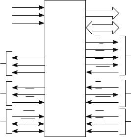
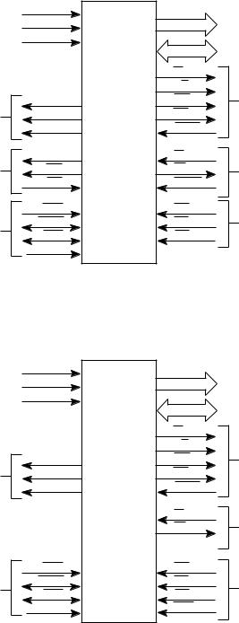
This section contains descriptions of the input and output signals. The input and output signals can be functionally organized into the groups shown in Figure 3-1 (for the
MC68000, the MC68HC000 and the MC68010), Figure 3-2 ( for the MC68HC001), Figure
3-3 (for the MC68EC000), Figure 3-4 (for the MC68008, 48-pin version), and Figure 3-5
(for the MC68008, 52-pin version). The following paragraphs provide brief descriptions of the signals and references (where applicable) to other paragraphs that contain more information about the signals.
NOTE
The terms assertion and negation are used extensively in this manual to avoid confusion when describing a mixture of "active-low" and "active-high" signals. The term assert or assertion is used to indicate that a signal is active or true, independently of whether that level is represented by a high or low voltage. The term negate or negation is used to indicate that a signal is inactive or false.
|
VCC(2) |
ADDRESS |
|
|
|
GND(2) |
|
||
|
BUS |
A23–A1 |
||
|
|
|||
|
CLK |
|
|
|
|
|
DATA BUS |
D15–D0 |
|
|
|
AS |
|
|
|
|
R/W |
ASYNCHRONOUS |
|
|
FC0 |
UDS |
||
PROCESSOR |
BUS |
|||
FC1 |
LDS |
CONTROL |
||
STATUS |
FC2 |
DTACK |
|
|
|
|
|||
MC6800 |
E |
BR |
BUS |
|
VMA |
BG |
|||
PERIPHERAL |
ARBITRATION |
|||
VPA |
|
|||
CONTROL |
BGACK |
CONTROL |
||
SYSTEM |
BERR |
IPL0 |
INTERRUPT |
|
RESET |
IPL1 |
|||
CONTROL |
CONTROL |
|||
HALT |
IPL2 |
|||
|
|
Figure 3-1. Input and Output Signals
(MC68000, MC68HC000 and MC68010)
MOTOROLA |
M68000 8-/16-/32-BIT MICROPROCESSORS USER'S MANUAL |
3-1 |
|
VCC(2) |
ADDRESS |
|
|
|
GND(2) |
|
||
|
BUS |
A23–A0 |
||
|
|
|||
|
CLK |
|
|
|
|
|
DATA BUS |
D15–D0 |
|
|
|
AS |
|
|
|
|
R/W |
ASYNCHRONOUS |
|
|
FC0 |
UDS |
||
PROCESSOR |
BUS |
|||
FC1 |
LDS |
CONTROL |
||
STATUS |
FC2 |
DTACK |
|
|
|
|
|||
MC6800 |
E |
BR |
BUS |
|
VMA |
BG |
|||
PERIPHERAL |
ARBITRATION |
|||
VPA |
|
|||
CONTROL |
BGACK |
CONTROL |
||
|
BERR |
IPL0 |
INTERRUPT |
|
SYSTEM |
RESET |
IPL1 |
||
CONTROL |
||||
CONTROL |
HALT |
IPL2 |
||
|
||||
|
MODE |
|
|
Figure 3-2. Input and Output Signals
(MC68HC001)
|
VCC(2) |
|
ADDRESS |
|
|
GND(2) |
|
|
|
|
|
BUS |
A23–A0 |
|
|
|
|
||
|
CLK |
|
|
|
|
|
|
DATA BUS |
D15–D0 |
|
|
|
AS |
|
|
|
|
R/W |
ASYNCHRONOUS |
|
FC0 |
|
UDS |
|
PROCESSOR |
|
BUS |
||
FC1 |
|
LDS |
CONTROL |
|
STATUS |
FC2 |
MC68EC000 |
DTACK |
|
|
|
|||
|
|
|
BR |
BUS |
|
|
|
BG |
ARBITRATION |
|
|
|
|
CONTROL |
|
BERR |
|
IPL0 |
|
SYSTEM |
RESET |
|
IPL1 |
INTERRUPT |
CONTROL |
HALT |
|
IPL2 |
CONTROL |
|
MODE |
|
AVEC |
|
Figure 3-3. Input and Output Signals
(MC68EC000)
3-2 |
M68000 8-/16-/32-BIT MICROPROCESSORS USER'S MANUAL |
MOTOROLA |