


PROGRAMMABLE LOGIC DESIGN: QUICK START HANDBOOK • CHAPTER 1
using the best gate configuration to minimize power, or using the FPGAfriendly, register-rich configuration for state machines.
You can easily experiment with different vendors, device families, and optimization constraints, thus exploring many different solutions instead of just one with the schematic approach.
To recap, the advantages of high level design and synthesis are many. It is much simpler and faster to specify your design using HLD, and much easier to make changes to the design because of the self-documenting nature of the language.
You are relieved from the tedium of selecting and interconnecting at the gate level. Merely select the library and optimization criteria (e.g., speed, area) and the synthesis tool will determine the results.
You can also try different design alternatives and select the best one for the application. In fact, there is no real practical alternative for designs exceeding 10,000 gates.
Intellectual Property (IP) Cores
IP cores are very complex pre-tested system-level functions that are used in logic designs to dramatically shorten development time.
The benefits of using an IP core include:
•Faster time to market
•A simplified development process
•Minimal design risk
•Reduced software compile time
•Reduced verification time
•Predictable performance/functionality.
IP cores are similar to vendor-provided soft macros in that they simplify the design specification step by removing designers from gate-level details of commonly used functions.
IP cores differ from soft macros in that they are generally much larger sys- tem-level functions, such as a PCI bus interface, DSP filter, or PCMCIA interface. They are extensively tested (and hence rarely free of charge) to prevent designers from having to verify the IP core functions themselves.
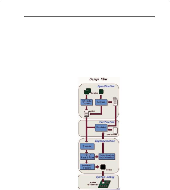
Design Verification
Programmable logic designs are verified by using a simulator, which is a software program that confirms the functionality or timing of a circuit.
The industry-standard formats used ensure that designs can be reused. If a vendors changes its libraries, only a synthesis recompile is necessary.
Xilinx • 14
INTRODUCTION
Even if you decide to move to a different vendor and/or technology, you’re just a compile away after selecting the new library. It’s even design-tool independent, so you can try synthesis tools from different vendors and pick the best results.
IP cores are more commonly available in HDL format, since that makes them easier to modify and use with different device vendors.
After completing the design specification, you’ll need to know if the circuit actually works as it’s supposed to. That is the purpose of design verification.
A simulator simulates the circuit. You’ll need to provide the design information (via the netlist after schematic capture or synthesis) and the specific input pattern, or test vectors, that you want checked. The simulator takes this information and determines the outputs of the circuit.
FIGURE 1-10: THE PLD DESIGN FLOW
Xilinx • 15

PROGRAMMABLE LOGIC DESIGN: QUICK START HANDBOOK • CHAPTER 1
Functional Simulation
At this point in the design flow, a functional simulation only checks that the circuits give the right combinations of ones and zeros. You would conduct a timing simulation a little later in the design flow.
If there are any problems, you can go back to the schematic or HDL file, make changes, re-generate the netlist, and then rerun the simulation. Designers typically spend 50% of their development time going through this loop until the design works as required.
Using HDL offers an additional advantage when verifying the design: You can simulate directly from the HDL source file. This bypasses the time-consum- ing synthesis process that would normally be required for every design change iteration.
Once the circuit works correctly, running the synthesis tool generates the netlist for the next step in the design flow – device implementation.
Device Implementation
A design netlist completely describes the design using the gates for a specific vendor/device family. Once it’s fully verified, it’s time to put this in a chip, referred to as device implementation.
Translate comprises various programs used to import the design netlist and prepare it for layout. The programs will vary among vendors.
Some of the more common programs during translate include: optimization, translation to the physical device elements, and device-specific design rule checking (e.g,. does the design exceed the number of clock buffers available in this device?).
During the stage of the design flow, you will be asked to select the target device, package, speed grade, and any other device-specific options.
The translate step usually ends with a comprehensive report of the results of all the programs executed. In addition to warnings and errors is usually a listing of device and I/O utilization, which helps you to determine if you’ve selected the best device.
Fitting
For CPLDs, the design step is called fitting, meaning to “fit” the design to the target device. In the diagram above, a section of the design is fit to the CPLD.
CPLDs are a fixed architecture, so the software needs to pick the gates and interconnect paths that match the circuit. This is usually a fast process.
The biggest potential problem is if you had previously assigned the exact locations of the I/O pins, commonly referred to as pin locking. Most often, this occurs when using a legacy design iteration that has been committed to the printed circuit board layout.
Architectures that support I/O pin locking (such as the Xilinx XC9500 and CoolRunner CPLDs) have a very big advantage. They allow you to keep the
Xilinx • 16

INTRODUCTION
original I/O pin placements regardless of the number of design changes, utilization, or required performance.
Pin locking is very important when using ISP. If you layout your PCB to accept a specific pin out, and then change the design, you can re-program confident that you pin out will stay the same.
Place and Route
For FPGAs, place and route programs are run after compile. “Place” is the process of selecting specific modules, or logic blocks, in the FPGAs where design gates will reside.
“Route,” as the name implies, is the physical routing of the interconnect between the logic blocks.
Most vendors provide automatic place and route tools so that you don’t have to worry about the intricate details of the device architecture. Some vendors offer tools that allow expert users to manually place and/or route the most critical parts of their designs to achieve better performance than with the automatic tools. Floorplanner is a type of manual tool.
Place and route programs require the longest time to complete successfully because it’s a complex task to determine the location of large designs, ensure that they all get connected correctly, and meet the desired performance.
These programs however, can only work well if the target architecture has sufficient routing for the design. No amount of fancy coding can compensate for an ill-conceived architecture, especially if there are not enough routing tracks.
If you were to encounter this problem, the most common solution would be to use a larger device. And you would likely remember the experience the next time you selected a vendor.
A related program is called timing-driven place and route (TDPR). This allows you to specify timing criteria that will be used during device layout.
A static timing analyzer is usually part of the vendor’s implementation software. It provides timing information about paths in the design. This information is very accurate and can be viewed in many different ways, such as displaying all paths in the design and ranking them from longest to shortest delay.
In addition, at this point you can use the detailed layout information after reformatting and go back to your chosen simulator with detailed timing information.
This process is called back-annotation and has the advantage of providing the accurate timing as well as the zeros and ones operation of your design.
In both cases, the timing reflects delays of the logic blocks as well as the interconnect.
The final implementation step is the download or program.
Xilinx • 17

PROGRAMMABLE LOGIC DESIGN: QUICK START HANDBOOK • CHAPTER 1
Downloading or Programming
Download generally refers to volatile devices such as SRAM FPGAs. As the name implies, you download the device configuration information into the device memory.
The bitstream that is transferred contains all the information to define the logic and interconnect of the design and is different for every design.
Because SRAM devices lose their configuration when the power is turned off, the bitstream must be stored somewhere for a production solution. A common such place is a serial PROM. There is an associated piece of hardware that connects from the computer to a board containing the target device.
Program is used to program all non-volatile programmable logic devices, including serial PROMs. Programming performs the same function as download, except that the configuration information is retained after the power is removed from the device.
For antifuse devices, programming can only be done once per device – hence the term one-time programmable.
Programming of Xilinx CPLDs can be done in-system via JTAG or with a conventional device programmer such as Data I/O.
JTAG Boundary Scan – formally known as IEEE/ANSI standard 1149.1_1190 – is a set of design rules that facilitate testing, device programming, and debugging at the chip, board, and system levels.
In-system programming has an added advantage in that devices can be soldered directly to the PCB (such as TQFP surface-mount-type devices). If the design changes, the devices do not need to be removed from the board but simply re-programmed in-system.
Xilinx • 18
INTRODUCTION
FIGURE 1-11: DEVICE IMPLEMENTATION – DOWNLOAD/PROGRAM
System Debug
The device is now working, but you still need to verify that the device works in the actual board, a process called system debug.
Any major problems here mean that you have made an assumption on the device specification that is incorrect, or have not considered some aspect of the signal required to/from the programmable logic device.
If so, you can collect data on the problem and go back to the drawing (or behavioral) board.
Xilinx has the world’s first WebPOWERED programmable logic devices. This means we have the first WebFITTER CPLD design fitting tool, enabling you to fit your design in real time at our website.
Simply take your existing design to our WebFITTER web page – these files can be HDL source code or netlists – and specify your target device or your key design criteria, such as speed or low power. Then press “fit.”
You will receive your results moments later via e-mail, which includes full fitter results, design files, and a programming file (JEDEC file). If you like the results, you can then obtain an online price.
You can download your personal copy in modules, so you can decide which parts you need. Modules include the design environment (Project Navigator), XST (Xilinx Synthesis Tool), ModelSim™ Xilinx Edition Starter (a thirdparty simulator), ChipViewer, and eventually ECS schematic capture and VSS.
Xilinx • 19

PROGRAMMABLE LOGIC DESIGN: QUICK START HANDBOOK • CHAPTER 1
Xilinx ChipViewer (a Java utility) graphically represents pin constraints and assignments. You can also use this tool to graphically view design implementations from the chip boundary to the individual macrocell equations.
Xilinx • 20