


PROGRAMMABLE LOGIC DESIGN: QUICK START HANDBOOK • CHAPTER 1
There are also costs associated with inventory and reliability. PLDs can reduce inventory costs by replacing standard discrete logic devices. Standard logic has a predefined function. In a typical design, lots of different types have to be purchased and stocked. If the design is changed, there may be excess stock of superfluous devices.
This issue can be alleviated by using PLDs. You only need to stock one device; if your design changes, you simply reprogram. By utilizing one device instead of many, your board reliability will increase by only picking and placing one device instead of many.
Reliability can also be increased by using ultra-low-power CoolRunner CPLDs. Their lower heat dissipation and lower power operation leads to decreased FIT.
Field Programmable Gate Arrays (FPGAs)
In 1985, a company called Xilinx introduced a completely new idea: combine the user control and time to market of PLDs with the densities and cost benefits of gate arrays.
Customers liked it – and the FPGA was born. Today Xilinx is still the num- ber-one FPGA vendor in the world.
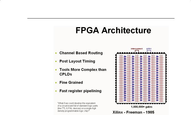
An FPGA is a regular structure of logic cells (or modules) and interconnect, which is under your complete control. This means that you can design, program, and make changes to your circuit whenever you wish.
With FPGAs now exceeding the 10 million gate limit (the Xilinx Virtex™-II FPGA is the current record holder), you can really dream big.
Xilinx • 6
INTRODUCTION
FIGURE 1-4: FPGA ARCHITECTURE
With the introduction of the Spartan series of FPGAs, Xilinx can now compete with gate arrays on all aspects – price, gate, and I/O count, as well as performance and cost.
The Spartan-IIE FPGA provides as many as 300,000 gates at a price point that enables application specific standard product (ASSP) replacement. For example, a Reed Solomon IP core implemented in a Spartan-II XC2S100 FPGA has an effective cost of $9.95, whereas the equivalent ASSP would cost around $20.
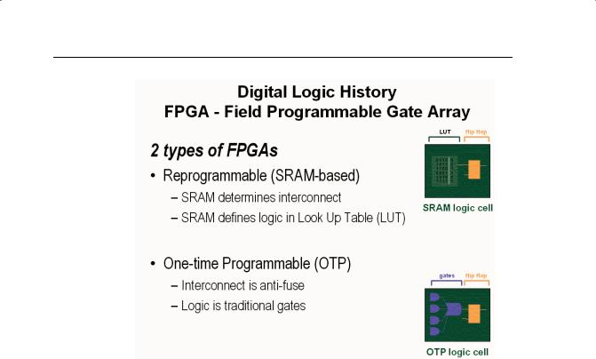
There are two basic types of FPGAs: SRAM-based reprogrammable and OTP. These two types of FPGAs differ in the implementation of the logic cell and the mechanism used to make connections in the device.
The dominant type of FPGA is SRAM-based and can be reprogrammed as often as you choose. In fact, an SRAM FPGA is reprogrammed every time it’s powered up, because the FPGA is really a fancy memory chip. That’s why you need a serial PROM or system memory with every SRAM FPGA.
Xilinx • 7
PROGRAMMABLE LOGIC DESIGN: QUICK START HANDBOOK • CHAPTER 1
FIGURE 1-5: DIGITAL LOGIC HISTORY
In the SRAM logic cell, instead of conventional gates, an LUT determines the output based on the values of the inputs. (In the “SRAM logic cell” diagram above, six different combinations of the four inputs determine the values of the output.) SRAM bits are also used to make connections.
OTP FPGAs use anti-fuses (contrary to fuses, connections are made, not “blown,” during programming) to make permanent connections in the chip. Thus, OTP FPGAs do not require SPROM or other means to download the program to the FPGA.
However, every time you make a design change, you must throw away the chip! The OTP logic cell is very similar to PLDs, with dedicated gates and flipflops.
DESIGN INTEGRATION
The integration of 74 series standard logic into a low-cost CPLD is a very attractive proposition. Not only do you save PCB area and board layers – thus reducing your total system cost – but you only have to purchase and stock one generic part instead of as many as 20 pre-defined logic devices.
In production, the pick and place machine only has to place one part, therefore speeding up production. Less parts means higher quality and better FIT factor.
Xilinx • 8