


CHA PT E R 5
Implementing CPLDs
Introduction
After you have successfully simulated your design, the synthesis stage converts the text-based design into an NGC netlist file.
The netlist is a non-readable file that describes the actual circuit to be implemented at a very low level.
The implementation phase uses the netlist and a constraints file to recreate the design using the available resources within the CPLD.
Constraints may be physical or timing and are commonly used for setting the required frequency of the design or declaring the required pinout.
The first step is translate. This step checks the design and ensures that the netlist is consistent with the chosen architecture. Translate also checks the UCF for any inconsistencies. In effect, this stage prepares the synthesized design for use within a CPLD.
The fit stage distributes the design to the resources in the CPLD and places those resources according to the constraints specified. Obviously, if the design is too big for the chosen device, the fit process will not be able to complete its job.
The fitter also uses the UCF file to understand timing and may sometimes decide to change the actual design.
For example, sometimes the fitter will change the D-Type flip-flops in the design to Toggle Type or T-Type registers. It all depends on how well the design converts into product terms.
Once the fitter has completed, it is good practice to re-simulate. As all the logic delays added by the macrocells, switch matrix, and flip-flops are known, MXE can use information for timing simulation.

PROGRAMMABLE LOGIC DESIGN -- QUICK START HANDBOOK • CHAPTER 5
The fitter creates a JEDEC file, which is used to program the device either on the board via a parallel cable or using programming equipment.
The steps of implementation must be carried out in this order.
WebPACK ISE software will automatically perform the steps required if a particular step is selected.
For example, if the design has only just been functionally simulated and you decide to do a timing simulation, the software will automatically synthesize, translate, and tit the design. It will then generate the timing information before it opens MXE and gives the timing simulation results.
The rest of this chapter demonstrates the steps required to successfully implement our traffic light design.
Synthesis
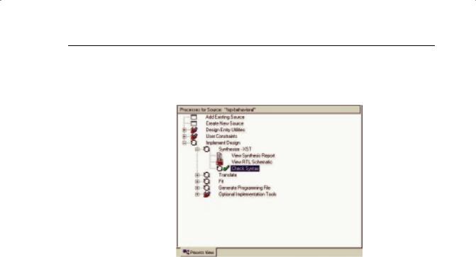
The XST synthesis tool will only attempt to synthesize the file highlighted in the Sources window.
In our traffic light design, “top.vhd” (for VHDL designs) or “top_sch” (for schematic designs) instantiates two lower level blocks, “stat_mac” and “counter.”
The synthesis tool recognizes all the lower level blocks used in the top-level code and synthesizes them together to create a single bitstream.
In the Sources window, ensure that “top.vhd” (or “top_sch” for schematic flows) is highlighted.
In the Process window, expand the Synthesis subsection by clicking on the “+” next to Synthesize.
You can now check your design by double-clicking on Check Syntax.
Ensure that any errors in your code are corrected before you continue. If the syntax check is OK, a tick will appear.
Xilinx • 132
IMPLEMENTING CPLDS
The design should be okay because both the HDL Bencher tool and MXE simulator have already checked for syntax errors. (It is useful, when writing code, to periodically check your design for any mistakes using this feature.)
FIGURE 5-1: PROCESS WINDOW SHOWING CHECK SYNTAX
Right-click on Synthesize and select Properties.
A window appears allowing you to influence the way in which your design is interpreted.
The Help feature will explain each of the options in each tab. Click on the
HDL Options tab.
In the Xilinx Specific Options tab, ensure that the Add IO Buffers box is ticked. The I/O buffers will be attached to all the port names in the top-level entity of the design.
Clicking on Help in each tab demonstrates the complex issue of synthesis and how the final result could change. The synthesis tool will never alter the function of the design, but it has a huge influence on how the design will perform in the targeted device.
Click OK in the Process Properties window and double-click on Synthesize.
When the synthesis is complete, a green tick will appear next to Synthesize. Double-click on View Synthesis Report.
Constraints Editor
To get the ultimate performance from the device, you must tell the implementation tools what and where performance is required.
This design is particularly slow and timing constraints are unnecessary.
Constraints can also be physical; pin locking is a physical constraint.
Xilinx • 133
PROGRAMMABLE LOGIC DESIGN -- QUICK START HANDBOOK • CHAPTER 5
For this design, assume that the specification for clock frequency is 100 MHz and that the pin-out has been pre-determined to that of a CoolRunner-II pre-designed board.
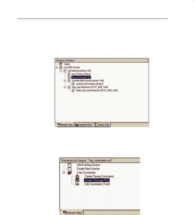
In the Source window, add a New Source of type Implementation Constraints File. Call this file “top_constraints “and associate it with the module “top.”
FIGURE 5-2: CONSTRAINTS FILE AS A SOURCE
In the Process window, expand the User Constraints section and doubleclick on Assign Package Pins.
FIGURE 5-3: ASSIGN PACKAGE PINS IN PACE TOOL
Xilinx • 134
IMPLEMENTING CPLDS
Notice that the translate step in the Implement Design section runs automatically. This is because the implementation stage must see the netlist before it can offer you the chance to constrain sections of the design.
When translate has completed, the Xilinx PACE (Pinout Area and Constraints Editor) tool opens.
If there are already constraints in the UCF file, these will be imported by PACE and displayed. As we have an empty UCF file, nothing exists for PACE to import.
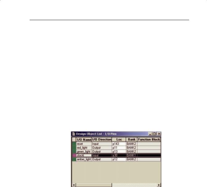
In the Design Object List, you can enter a variety of constraints on the I/O pins used in the design. PACE recognizes the five pins in the design and displays them in the list.
Click in the Loc area next to each signal and enter the following location constraints:
clock p38
reset p143
red_light p11
green_light p13
amber_light p12
FIGURE 5-4: ENTER LOCATION CONSTRAINTS
When a pin is highlighted in the Design Object List, the pin to which it is “Loc'ed” is highlighted in the Package Pins view.
Save the PACE session and exit the PACE tool.
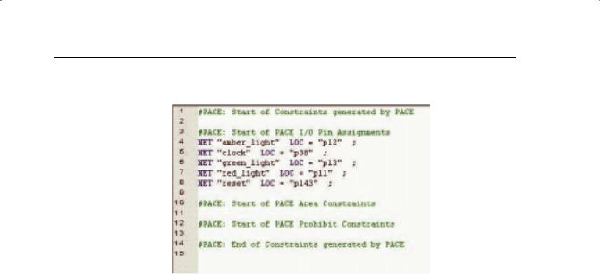
It is now possible to see the constraints in the UCF file.
With “top_constraints.ucf” highlighted in the Source window, double-click
Edit Constraints (Text) in the Process window.
The UCF file will open in the main window of the ISE Project Navigator.
Xilinx • 135
PROGRAMMABLE LOGIC DESIGN -- QUICK START HANDBOOK • CHAPTER 5
The constraints entered into PACE can be seen in Figure 5-5.
FIGURE 5-5: TEXT CONSTRAINTS IMPORTED FROM PACE
To force a signal onto a global resource, you can apply the BUFG constraint. In this case, we will apply the BUFG constraint to the clock signal.
Enter the following syntax in the text file:
NET "clock" BUFG=CLK;
Save and close the text file.
The next step is to create timing constraints. With the UCF highlighted in the Source window, double-click on Create Timing Constraints in the Process window.
The Constraints Editor will open. This tool can be used to set location constraints, but for this tutorial it will only be used to create timing constraints.
The Constraints Editor recognizes the one global signal in the design.
Xilinx • 136
IMPLEMENTING CPLDS
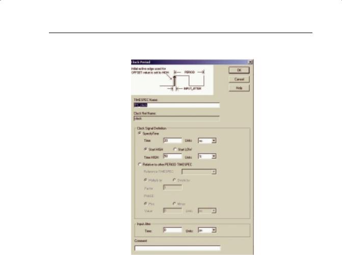
DoubLe-click in the Period window of the global clock signal.
FIGURE 5-6: CLOCK PERIOD EDITOR WINDOW
In the Clock Period definition window, change the Time value to 10 ns. The duty cycle should stay at 50% high, 50% low.
The period constraint is now written into the UCF file and can be seen in the constraints list at the bottom of the Constraints Editor.
A period constraint ensures that the internal paths starting and ending at synchronous points (flip-flop, latch) have a logic delay less than 10 ns.
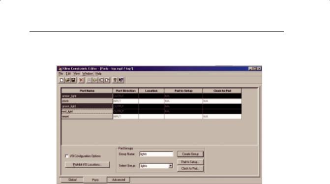
Click the Ports tab in the Constraints Editor. As there were already constraints in the UCF, they have been imported.
Xilinx • 137
PROGRAMMABLE LOGIC DESIGN -- QUICK START HANDBOOK • CHAPTER 5
Highlight the three outputs “red_light,” “green_light,” and “amber_light” using ctrl select.
FIGURE 5-7: CONSTRAINTS EDITOR – CREATE GROUP
In the Group Name field, type “lights” and then click the Create Group but-
ton.
In the Select Group box, select “lights” and click the Clock to Pad button.
Xilinx • 138
IMPLEMENTING CPLDS
In the Clock to Pad dialog box, set the Time Requirement to 15 ns relative to the clock. (There is only one clock, but in some designs there may be more).
FIGURE 5-8: CLOCK TO PAD DIALOG BOX
Click OK.
Notice that the Clock to Pad fields have been filled in automatically and that the UCF generated has appeared in the UCF constraints tab at the bottom of the screen.
The UCF file should look similar to Figure 5-9.
FIGURE 5-9: COMPLETE CONSTRAINTS LIST
Xilinx • 139

PROGRAMMABLE LOGIC DESIGN -- QUICK START HANDBOOK • CHAPTER 5
Save the Constraints Editor session and exit the Constraints Editor.
CoolRunner-II architecture supports the use of non 50:50 duty cycle clocks by implementing input hysteresis. This can be selected on a pin-by-pin basis.
For example, if the clock used in this design is an RC oscillator, the input hysteresis can be used to clean up the clock using the following constraint syntax:
NET “clock” schmitt_trigger;
The CoolRunner-II CPLD also supports different I/O standards.
If the three light signals had to go to a downstream device that required the signals to conform to a certain I/O standard, you could use the following constraint syntax:
NET “red_light” IOSTANDARD=LVTTL;
The permissible standards are LVTTL, LVCMOS15, LVCMOS18, LVCMOS25, LVCMOS33. On larger devices (128 macrocell and larger), the permissible standards are HSTL_I, SSTL2_I, and SSTL3_I.
However, you can use only one I/O standard per bank, so take care when assigning different I/O standards in a design.
The CoolRunner-II family has several features that are aimed at reducing power consumption in the device.
One of these features is known as CoolClock. The clock signal on Global Clock Input 2 (GCK2) is divided by 2 as soon as it enters the device.
All of the registers clocked by this clock are then automatically configured as dual-edge triggered flip-flops.
The highest toggling net in the design will now be toggling at half the frequency, which will reduce the power consumption of that net without compromising the performance of the design.
The CoolClock attribute can be applied by right-clicking on GCK2 in ChipViewer or by adding the following line in the UCF:
NET “clock” COOL_CLK;
However, we will not use these features in this tutorial.
For more information on the use of CoolRunner-II CPLDs, and their advanced features, visit www.xilinx.com/apps/epld.htm for a number of application notes, often including free code examples.
You must re-run translate so the new constraints can be read.
Xilinx • 140
IMPLEMENTING CPLDS
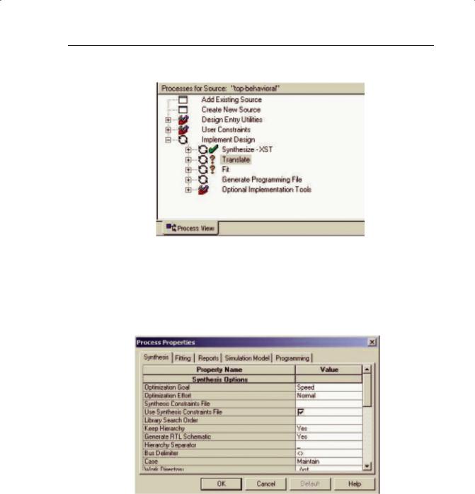
Click on the “+” next to Implement Design in the Process window.
FIGURE 5-10: DESIGN PROCESS WINDOW
The implementation steps are now visible. An orange question mark indicates that translate is now out of date and should be re-run.
A right-click on Implement Design allows you to edit the properties for each particular step.
FIGURE 5-11: PROCESS PROPERTIES – IMPLEMENT DESIGN
The Help button will explain the operation of each field.
You can set the default I/O standard under the Fitting tab of the Process Properties window, as shown in Figure 5-11.
Xilinx • 141