![](/user_photo/2706_HbeT2.jpg)
- •Navigating This Book
- •Table of Contents
- •Introduction
- •The History of Programmable Logic
- •Complex Programmable Logic Devices (CPLDs)
- •Why Use a CPLD?
- •Field Programmable Gate Arrays (FPGAs)
- •Design Integration
- •The Basic Design Process
- •HDL File Change Example
- •Before (16 x 16 multiplier):
- •After (32 x 32 multiplier):
- •Intellectual Property (IP) Cores
- •Design Verification
- •Xilinx Solutions
- •Introduction
- •Xilinx Devices
- •Platform FPGAs
- •Virtex FPGAs
- •Virtex-II Pro FPGAs
- •Virtex FPGAs
- •Spartan FPGAs
- •Spartan-3 FPGAs
- •Spartan-IIE FPGAs
- •Spartan-IIE Architectural Features
- •Xilinx CPLDs
- •XC9500 ISP CPLD Overview
- •XC9500XL 3.3V Family
- •XC9500XV 2.5V CPLD Family
- •CoolRunner Low-Power CPLDs
- •CoolRunner-II CPLDs
- •CoolRunner Reference Designs
- •Military and Aerospace
- •Automotive and Industrial
- •Design Tools
- •Design Entry
- •Synthesis
- •Implementation and Configuration
- •Board-Level Integration
- •Verification Technologies
- •Advanced Design Techniques
- •Embedded SW Design Tools Center
- •Xilinx IP Cores
- •Web-Based Information Guide
- •End Markets
- •Silicon Products and Solutions
- •Design Resources
- •System Resources
- •Xilinx Online (IRL)
- •Configuration Solutions
- •Processor Central
- •Tools and Partnerships
- •Memory Corner
- •Silicon
- •Design Tools and Boards
- •Technical Literature and Training
- •Connectivity Central
- •High-Speed Design Resources
- •Signal Integrity Tools
- •Partnerships
- •Signal Integrity
- •Services
- •Xilinx Design Services
- •Education Services
- •Live E-Learning Environment
- •Day Segment Courses
- •Computer-Based Training (CBT)
- •University Program
- •Design Consultants
- •Technical Support
- •Module Descriptions
- •WebPACK Design Suite
- •WebPACK Design Entry
- •WebPACK StateCAD
- •WebPACK MXE Simulator
- •WebPACK HDL Bencher Tool
- •WebPACK FPGA Implementation Tools
- •WebPACK CPLD Implementation Tools
- •WebPACK iMPACT Programmer
- •WebPACK ChipViewer
- •XPower
- •WebPACK CD-ROM Installation
- •Getting Started
- •Licenses
- •Projects
- •Summary
- •Introduction
- •Design Entry
- •The Language Template
- •Close the Language Templates
- •Edit the Counter Module
- •Save the Counter Module
- •Functional Simulation
- •State Machine Editor
- •Top-Level VHDL Designs
- •Top-Level Schematic Designs
- •ECS Hints
- •I/O Markers
- •Implementing CPLDs
- •Introduction
- •Synthesis
- •Constraints Editor
- •CPLD Reports
- •Timing Simulation
- •Configuration
- •Implementing FPGAs
- •Introduction
- •Synthesis
- •The Constraints File
- •FPGA Reports
- •Programming
- •Summary
- •Design Reference Bank
- •Introduction
- •Get the Most out of Microcontroller-Based Designs
- •Conventional Stepper Motor Control
- •Using a Microcontroller to Control a Stepper Motor
- •Stepper Motor Control Using a CPLD
- •PC-Based Motor Control
- •Design Partitioning
- •Conclusion
- •Documentation and Example Code
- •Website Reference
- •ACRONYMS
- •GLOSSARY OF TERMS
![](/html/2706/360/html_VlCnZR7m53.iSY_/htmlconvd-3KC6_4165x1.jpg)
IMPLEMENTING FPGAS
The Constraints File
To get the ultimate performance from the device, you must tell the implementation tools what and where performance is required.
This design is particularly slow and timing constraints are unnecessary.
Constraints can also be physical; pin locking is a physical constraint.
For this design, assume that the specification for clock frequency is 100 MHz and that the pin-out has been pre-determined to that of a Spartan-3 device.
There are already some constraints in the UCF from the previous project implementation. It will be necessary to delete these constraints.
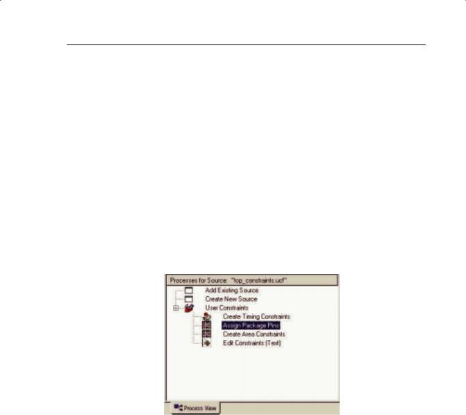
Highlight “top_constraints.ucf” in the Source window. Expand the “+” next to User Constraints and double-click Edit Constraints (Text).
Highlight all of the constraints and delete them. Save the UCF and close it.
Double-click on Assign Package Pins.
Alternatively, you can highlight the top level (“top.vhd”) and expand the User Constraints branch.
FIGURE 6-5: PROCESS WINDOW SHOWING ASSIGN PACKAGE PINS
The PACE tool will be launched.
Assign all I/O pins in the Design Object List as follows.
reset |
p36 |
red_light |
p44 |
green_light |
p52 |
clock |
p55 |
amber_light |
p46 |
|
|
Xilinx • 153
![](/html/2706/360/html_VlCnZR7m53.iSY_/htmlconvd-3KC6_4166x1.jpg)
PROGRAMMABLE LOGIC DESIGN -- QUICK START HANDBOOK • CHAPTER 6
Save and Exit the PACE session.
Double-click on Create Timing Constraints in the Process window, as seen above Assign Package Pins in Figure 6-5.
Notice that the Constraints Editor is invoked and picks up the LOC constraints entered in PACE.
These can be edited by double-clicking on them in the read-write window or under the Ports tab in the Main window.
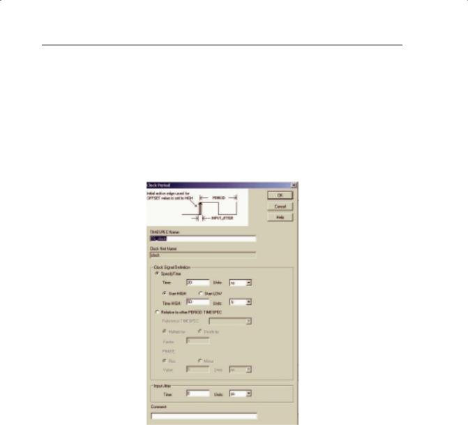
Double-click in the Period window of the global signal clock and enter a period of 10 ns.
FIGURE 6-6: SPECIFY PERIOD CONSTRAINT
Click OK.
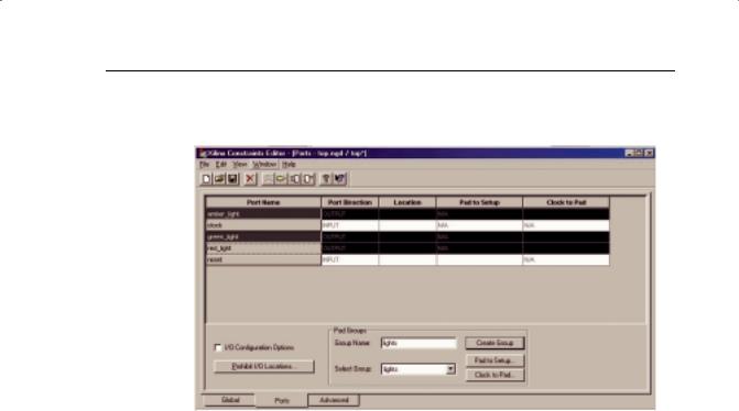
Click on the Ports tab in the Constraints Editor. As there were already constraints in the UCF, they have been imported.
Xilinx • 154
![](/html/2706/360/html_VlCnZR7m53.iSY_/htmlconvd-3KC6_4167x1.jpg)
IMPLEMENTING FPGAS
Highlight the three outputs “red_light,” “green_light,” and “amber_light” using ctrl select.
FIGURE 6-7: CONSTRAINTS EDITOR – CREATE GROUP
In the Group Name field, type “lights” and then hit Create Group. In the Select Group box, select lights and hit the Clock to Pad button.
Xilinx • 155
![](/html/2706/360/html_VlCnZR7m53.iSY_/htmlconvd-3KC6_4168x1.jpg)
PROGRAMMABLE LOGIC DESIGN -- QUICK START HANDBOOK • CHAPTER 6
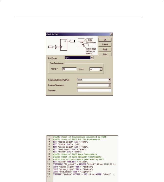
In the Clock to Pad dialog box, set the time requirement to 15 ns relative to the clock. There is only one clock, but in some designs there may be more.
FIGURE 6-8: CLOCK TO PAD DIALOG BOX
Click OK.
Notice that the Clock to Pad fields have been filled in automatically. Also notice that the UCF generated has appeared in the UCF Constraints tab at the bottom of the screen.
The UCF file should look similar to Figure 6-9.
FIGURE 6-9: COMPLETE CONSTRAINTS FILE
Xilinx • 156
![](/html/2706/360/html_VlCnZR7m53.iSY_/htmlconvd-3KC6_4169x1.jpg)
IMPLEMENTING FPGAS
Save and close the Constraints Editor session.
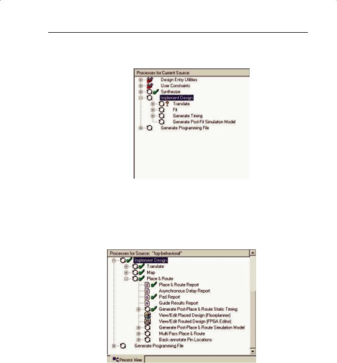
Click on the “+” next to Implement Design in the Process window.
FIGURE 6-10: PROCESS WINDOW SHOWING IMPLEMENT DESIGN
Implement the design by double-clicking on Implement Design. (You could run each stage separately if required.)
When there is a green tick next to Translate, Map, and Place and Route, your design has completed the implementation stage.
FIGURE 6-11: COMPLETED IMPLEMENTATION
A green tick means that the design ran through without any warnings.
Xilinx • 157