

WEBPACK ISE DESIGN ENTRY
You are now ready to go to the implementation stage.
Top-Level Schematic Designs
Sometimes, it’s easier to visualize designs when they have a schematic top level that instantiates the individual blocks of HDL. The blocks can then be wired together in the traditional method.
For designs in the WebPACK ISE tool, the entire project can be schematicbased.
This section discusses the method of connecting VHDL modules via the ECS schematic tool.
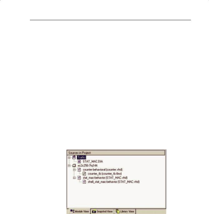
If you have worked through the previous session, you will first need to revert to the screen shown in Figure 4-32 (two modules with no top-level file).
At the bottom of the Sources window, select the Snapshot View tab.
Highlight Snap2 (two modules). In the Project menu, select Make Snapshot Current.
This action will take you back to the stage in the flow with only the “counter.vhd” and the “stat_mac.vhd” files.
WebPACK ISE software will ask if you would like to take another snapshot of the design in its current state.
Select Yes and create a third snapshot called “vhdl_top.”
The Sources window module view should look like Figure 4-32.
FIGURE 4-32: SOURCES IN PROJECT WINDOW
ECS HINTS
The ECS schematic capture program is designed around you selecting the action you wish to perform, followed by the object on which the action will be performed.
Xilinx • 125
PROGRAMMABLE LOGIC DESIGN -- QUICK START HANDBOOK • CHAPTER 4
In general, most Windows applications currently operate by selecting the object and then the action to be performed on that object.
Understanding this fundamental philosophy of operation makes learning ECS a much more enjoyable experience.
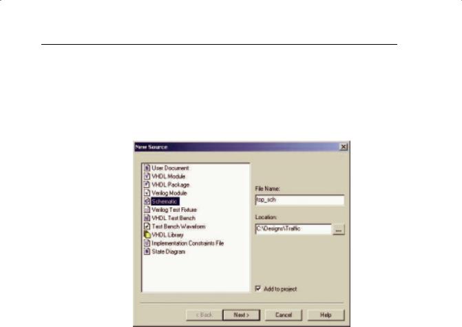
From the Project menu, select New Source > Schematic and give it the name “top_sch.”
FIGURE 4-33: NEW SOURCE WINDOW SHOWING TOP_SCH
Click the Next> button, then the Finish button.
The ECS Schematic Editor window will now appear.
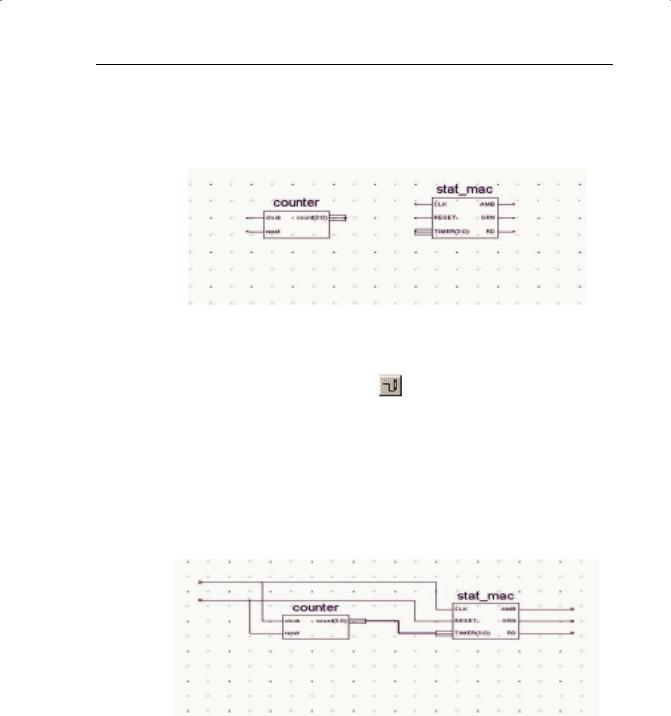
Back in the Project Navigator, highlight “counter.vhd” in the Sources window.
In the Process window, double-click on Create Schematic Symbol from the Design Entry Utilities section. This will create a schematic symbol and add it to the library in the Schematic Editor.
Create another symbol – this time for the state machine – by highlighting “stat_mac.vhd” and double-clicking on Create Schematic Symbol.
Returning to the Schematic editor, the symbol libraries can be found under the Symbol tab on the left-hand side of the page.
Add the counter and state machine by clicking on the new library in the Categories window at the top right of the ECS page and then selecting Counter.
Move the cursor over the sheet and drop the counter symbol by clicking where it should be placed.
Xilinx • 126
WEBPACK ISE DESIGN ENTRY
Move the cursor back into the Categories window and place the “stat_mac” symbol on the sheet.
Zoom in using the button so your zoom button and the window looks like Figure 4-34.
FIGURE 4-34: CLOSE-UP OF COUNTER AND STATE MACHINE SYMBOLS
Select the Add Wire tool from the Drawing toolbar.
To add a wire between two pins, click once on the symbol pin, once at each vertex, and once on the destination pin.
ECS will let you decide whether to use the Autorouter or manually place the signals on the page.
To add a hanging wire, click on the symbol pin to start the wire once at each vertex. Then double-click at the location where you want the wire to terminate.
Wire up the counter and state machine as shown in Figure 4-35:
FIGURE 4-35: COUNTER AND STATE MACHINE SYMBOLS WITH WIRE
Xilinx • 127
PROGRAMMABLE LOGIC DESIGN -- QUICK START HANDBOOK • CHAPTER 4
Select the Add Net Names tool from the Drawing toolbar.
Type “clock” (notice that the text appears in the window in the top lefthand side of the ECS page) and then place the net name on the end of the clock wire.
To add net names to wires that will be connected to your FPGA/CPLD I/Os, place the net name on the end of the hanging wire.
Finish adding net names so that your schematic looks similar to Figure 4-36.
FIGURE 4-36: MORE NET NAMES
ECS recognizes that count(3:0) and TIMER(3:0) are buses, and so connects them together with a bus rather than a single net.
I/O MARKERS
Select the Add I/O Marker tool from the Drawing toolbar.
With the Input type selected, click and drag around all the inputs to which you want to add input markers.
Repeat for the outputs but select Output type.
Xilinx • 128
WEBPACK ISE DESIGN ENTRY
Your completed schematic should look like Figure 4-37.
FIGURE 4-37: ADDING I/O MARKERS
Save the design and exit the Schematic editor.
(In the Design Entry utilities, you can view the VHDL created from the schematic when “top_sch” is selected in the Sources window. The synthesis tool actually works from this file.)
You can now simulate the entire design.
Highlight “top_sch.sch” in the Sources window.
Add a new testbench waveform source by right-clicking on “top_sch.sch” and selecting New Source. Call this source “top_sch_tb” and associate it with “top.”
Accept the timing in the Initialize Timing dialog box and click OK.
In the waveform diagram, enter the input stimulus as follows:
Set the RESET cell below CLK cycle 1 to a value of “1.”
Click the RESET cell below CLK cycle 2 to reset it low.
Xilinx • 129
PROGRAMMABLE LOGIC DESIGN -- QUICK START HANDBOOK • CHAPTER 4
Go to the 64th clock cycle, right-click and select Set End of
Testbench.
FIGURE 4-38: Waveform Diagram
Close the Edit Test Bench window.
Click the Save Waveform button.
Close the HDL Bencher tool.
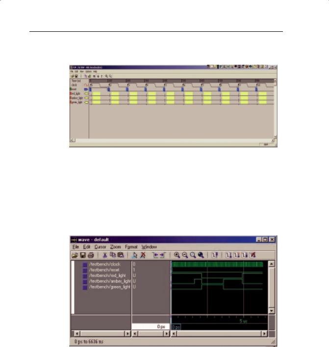
With “top_sch_tb.tbw” selected in the Sources window, expand ModelSim simulator and double-click Simulate Behavioral VHDL Model in the Process window.
FIGURE 4-39: MODELSIM SIMULATION WINDOW
You are now ready to go to the implementation stage.
Xilinx • 130