

INTRODUCTION
By using Xilinx CoolRunner devices, you can benefit from low power consumption and reduced thermal emissions. This in turn leads to the reduction of the use of heat sinks (another cost savings) and a higher reliability end product.
FIGURE 1-6: BASIC LOGIC DEFINITIONS
The Basic Design Process
The availability of products such as WebPACK ISE software has made it much easier to design with programmable logic. Designs can be described easily and quickly using a description language such as ABEL, VHDL, Verilog™, or with a schematic capture package.
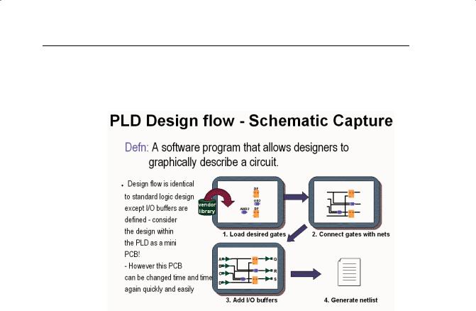
Schematic capture is the traditional method that designers have used to specify gate arrays and programmable logic devices. It is a graphical tool that allows you to specify the exact gates required and how you want them connected. There are four basic steps to using schematic capture:
1.After selecting a specific schematic capture tool and device library, begin building the circuit by loading the desired gates from the selected library. You can use any combination of gates that you need. You must choose a specific vendor and device family library at this time, but you don’t yet have to know what device within that family you will ultimately use with respect to package and speed.
2.Connect the gates together using nets or wires. You have complete control of connecting the gates in whatever configuration is required for your application.
Xilinx • 9
PROGRAMMABLE LOGIC DESIGN: QUICK START HANDBOOK • CHAPTER 1
3.Add and label the input and output buffers. These will define the I/O package pins for the device.
4.Generate a netlist.
FIGURE 1-7: PLD DESIGN FLOW
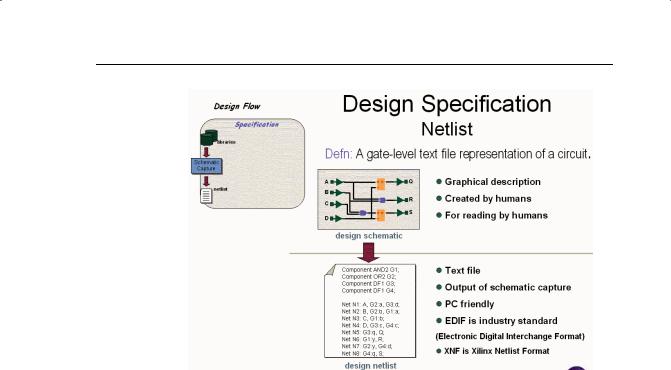
A netlist is a text equivalent of the circuit. It is generated by design tools such as a schematic capture program. The netlist is a compact way for other programs to understand what gates are in the circuit, how they are connected, and the names of the I/O pins.
In the example below, the netlist reflects the actual syntax of the circuit in the schematic. There is one line for each of the components and one line for each of the nets. Note that the computer assigns names to components (G1 to G4) and to the nets (N1 to N8). When implementing this design, it will have input package pins A, B, C, and D, and output pins Q, R, and S.
EDIF is the industry-wide standard for netlists; many others exist, including vendor-specific ones such as the Xilinx Netlist Format (XNF).
Once you have the design netlist, you have all you need to determine what the circuit does.
Xilinx • 10
INTRODUCTION
FIGURE 1-8: DESIGN SPECIFICATION – NETLIST
The example on the previous pages is obviously very simplistic. Let’s describe a more realistic design of 10,000 equivalent gates.
The typical schematic page contains about 200 gates, contained with soft macros. Therefore, it would require 50 schematic pages to create a 10,000-gate design! Each page needs to go through all the steps mentioned previously: adding components, interconnecting the gates, adding I/Os, and generating a netlist. This is rather time-consuming, especially if you want to have a 20,000, 50,000, or even larger design.
Another inherent problem with using schematic capture is the difficulty in migrating between vendors and technologies. If you initially create your 10,000gate design with FPGA vendor X and then want to migrate to a gate array, you would have to modify every one of those 50 pages using the gate array vendor’s component library.
There has to be a better way ... and of course, there is. It’s called high-level design (HLD), behavioral, or hardware description language (HDL). For our purposes, these three terms are essentially the same thing.
The idea is to use a high-level language to describe the circuit in a text file rather than a graphical low-level gate description. The term behavioral is used because in this powerful language, you describe the function or behavior of the circuit in words rather than figuring out the appropriate gates needed to create the application.
There are two major flavors of HDL: VHDL and Verilog.
Xilinx • 11
PROGRAMMABLE LOGIC DESIGN: QUICK START HANDBOOK • CHAPTER 1
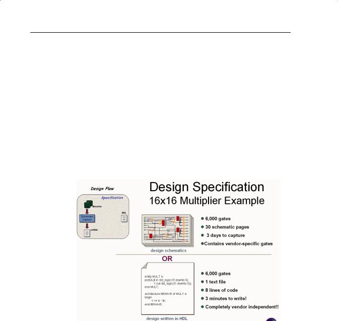
As an example, let’s design a 16 x 16 multiplier specified with a schematic capture and an HDL file.
A multiplier is a regular but complex arrangement of adders and registers that requires quite a few gates. Our example has two 16-bit inputs (A and B) and a 32-bit product output (Y = A x B) – that’s a total of 64 I/Os. This circuit requires approximately 6,000 equivalent gates.
In the schematic implementation, the required gates would have to be loaded, positioned on the page, and interconnected, with I/O buffers added. That’s about three days’ worth of work.
The HDL implementation, which is also 6,000 gates, requires eight lines of text and can be done in three minutes. This file contains all the information necessary to define our 16 x 16 multiplier.
So, as a designer, which method would you choose? In addition to the tremendous time savings, the HDL method is completely vendor-independent. This opens up tremendous design possibilities for engineers.
FIGURE 1-9: DESIGN SPECIFICATION – MULTIPLIER
To create a 32 x 32 multiplier, you could simply modify the work you’d already done for the smaller multiplier.
For the schematic approach, this would entail making three copies of the 30 pages, then figuring out where to edit the 90 pages so that they addressed the larger bus widths. This would probably require four hours of graphical editing.
Xilinx • 12