


XILINX SOLUTIONS
•Mainstream, scalable, high-reliability processing
•Fast ISP and erase times
Outperforms All Other 3.3V CPLDs
•Extended data retention supports longer system operating life
•Virtually eliminates ISP failures
•Superior pin-locking for lower design risk
•Glitch-free I/O pins during power-up
•Full IEEE 1149.1 (JTAG) ISP and Boundary Scan testing
•Free WebPOWERED software
XC9500XV 2.5V CPLD FAMILY
The Xilinx XC9500XV 2.5V CPLD family is based on an advanced architecture that combines system flexibility and low cost to allow for faster time to market and lower manufacturing and support costs.
Designed to operate with an internal core voltage of 2.5V, the XC9500XV silicon offers 30% lower power consumption than 3.3V CPLDs, resulting in lower heat dissipation and increased long-term device reliability.
The XC9500XV silicon plus the powerful WebPOWERED software offers a valuable logic solution that can't be beat when it comes to cost and ease of use.
High Performance Through Advanced Technology
Manufactured on the latest generation 0.25 µm process, the new XC9500XV CPLDs provide the same advanced architectural features and densities of the 3.3V XC9500XL family, with device offerings of 36, 72, 144, and 288 macrocells.
A high-performance version offering pin-to-pin delays as low as 3.5 ns and system frequencies as fast as 275 MHz will be available later this year.
The 2.5V XC9500XV devices also include optimized support for ISP through the industry's most extensive IEEE1149.1 JTAG and IEEE 1532 programming capability, which helps to streamline the manufacturing, testing, and programming of CPLD-based electronic products, including remote field upgrades.
The System Designer’s CPLD
The advanced architecture employed in the XC9500XV CPLD allows for easy design integration, thus empowering you to fully concentrate on your system design and not so much on chip-level details.
The unique features offered in the XC9500XV include a 54-input block fanin, which contributes to the device's superior pin-locking capability; built-in input hysteresis for improved noise margin; bus-hold circuitry for better I/O control; hot-plugging capability to eliminate the need for power sequencing; and local and global clock control to provide maximum flexibility.
Xilinx • 45
PROGRAMMABLE LOGIC DESIGN: QUICK START HANDBOOK • CHAPTER 2
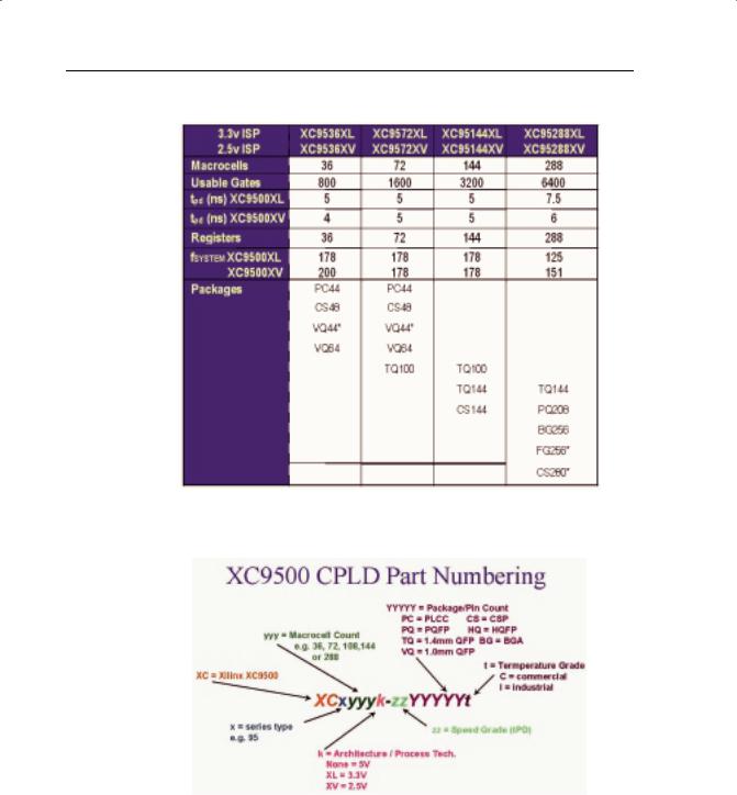
TABLE 2-3: XC9500XV AND XC9500XL PRODUCT SELECTION
FIGURE 2-20: XC9500 PART NUMBERING SYSTEM
Xilinx • 46
XILINX SOLUTIONS
COOLRUNNER LOW-POWER CPLDS
There are two members to the CoolRunner series, CoolRunner XPLA3 device (3.3V) and the CoolRunner-II (1.8V) device. Let’s look at the CoolRunner XPLA3 devices.
CoolRunner CPLDs combine very low power with high speed, high density, and high I/O counts in a single device. The CoolRunner 3.3V family ranges in density from 32 to 512 macrocells.
CoolRunner CPLDs feature Fast Zero Power technology, allowing the devices to draw virtually no power in standby mode. This makes them ideal for the fast-growing market of battery-operated portable electronic equipment, such as:
•Laptop PCs
•Telephone handsets
•Personal digital assistants
•Electronic games
•Web tablets.
These CPLDs also use far less dynamic power during actual operation compared to conventional CPLDs, an important feature for high-performance, heatsensitive equipment such as telecom switches, video conferencing systems, simulators, high-end testers, and emulators.
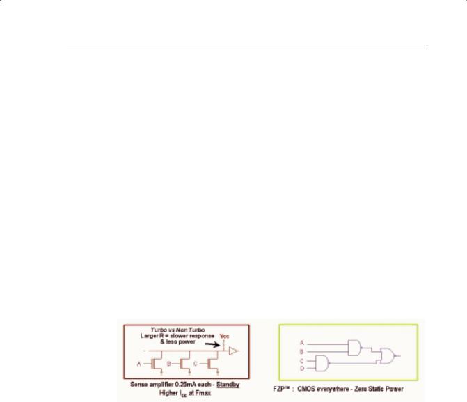
FIGURE 2-21: SENSE AMPLIFIER VS. CMOS CPLDS
The CoolRunner XPLA3 eXtended family of CPLDs is targeted for lowpower applications that include portable, handheld, and power-sensitive applications.
Each member of the XPLA3 family includes Fast Zero Power design technology that combines low power and high speed. With this design technique, the XPLA3 family offers true pin-to-pin speeds of 5.0 ns, while simultaneously delivering power that is <100 µA (standby) without the need for special "power down bits" that can negatively affect device performance.
By replacing conventional amplifier methods for implementing product terms (a technique that has been used in PLDs since the bipolar era) with a cas-
Xilinx • 47
PROGRAMMABLE LOGIC DESIGN: QUICK START HANDBOOK • CHAPTER 2
caded chain of pure CMOS gates, the dynamic power is also substantially lower than any competing CPLD.
CoolRunner devices are the only total CMOS PLDs, as they use both a CMOS process technology and the patented full CMOS Fast Zero Power design technique.
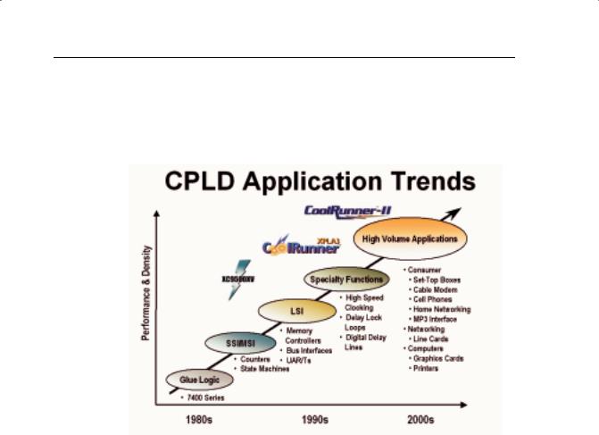
FIGURE 2-22: CPLD APPLICATION TRENDS
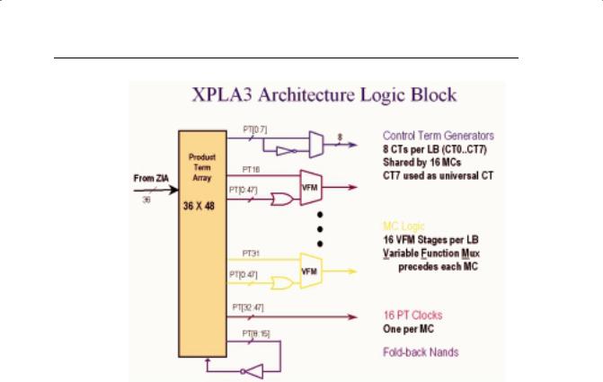
XPLA3 Architecture
The XPLA3 architecture features a direct input register path, multiple clocks, JTAG programming, 5V-tolerant I/Os, and a full PLA structure. These enhancements deliver high speed coupled with flexible logic allocation, which results in the ability to make design changes without changing pin-outs.
The XPLA3 architecture includes a pool of 48 product terms that can be allocated to any macrocell in the logic block. This combination allows logic to be allocated efficiently throughout the logic block and support as many product terms as needed per macrocell. In addition, using a variable number of product terms per macrocell incurs no speed penalty.
The XPLA3 family features industry-standard IEE 1149.1 JTAG interface, through which (ISP) and reprogramming of the device can occur. The XPLA3 CPLD is electrically reprogrammable using industry-standard device programmers from vendors such as Data I/O, BP Microsystems, and SMS.
Xilinx • 48
XILINX SOLUTIONS
Figure 2-23 shows a high-level block diagram of the XPLA3 architecture. The XPLA3 architecture comprises logic blocks inter-connected by ZIA. The ZIA is a virtual cross point switch. Each logic block has 36 inputs from the ZIA and 16 macrocells.
From this point of view, this architecture looks like many other CPLD architectures. What makes the XPLA3 family unique is logic allocation inside each logic block and the design technique used to implement these logic blocks.
FIGURE 2-23: COOLRUNNER XPLA3 ARCHITECTURE OVERVIEW
Logic Block Architecture
Figure 2-24 illustrates the logic block architecture of CoolRunner XPLA CPLDs.
Each logic block contains a PLA array that generates control terms and macrocells for use as asynchronous clocks, resets, presets, and output enables.
The other p-terms serve as additional single inputs into each macrocell. There are eight FoldBack NAND p-terms that are available for ease of fitting and pin locking.
Sixteen product terms are coupled with the associated programmable OR gate into the VFM. The VFM increases logic optimization by implementing any two input logic functions before entering the macrocell.
Xilinx • 49
PROGRAMMABLE LOGIC DESIGN: QUICK START HANDBOOK • CHAPTER 2
FIGURE 2-24: COOLRUNNER XPLA3 LOGIC BLOCK
Each macrocell supports combinatorial or registered inputs, preset and reset, configurable D, T, or latch functions. If a macrocell needs more product terms, it simply gets the additional product terms from the PLA array.
FoldBack NANDs
XPLA3 utilizes FoldBack NANDs to increase the effective product term width of a programmable logic device. These structures effectively provide an inverted product term to be used as a logic input by all of the local product terms.
Xilinx • 50
XILINX SOLUTIONS
Macrocell Architecture
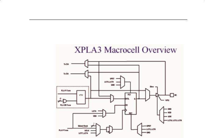
Figure 2-25 shows the architecture of a macrocell used in the CoolRunner XPLA3 CPLD. Any macrocell can be reset or pre-set on power-up.
FIGURE 2-25: COOLRUNNER XPLA3 MACROCELL DIAGRAM
Each macrocell register can be configured as a D-, T-, or latch-type flip-flop, or combinatorial logic function. Each of these flip-flops can be clocked from any one of eight sources.
Two global synchronous clocks are derived from the four external clock pins. There is one universal clock signal. You can individually configure the clock input signals CT[4:7] (local control terms) as either a PRODUCT term or SUM term equation created from the 36 signals available inside the logic block.
There are two feedback paths to the ZIA: one from the macrocell and one from the I/O pin. Using the I/O pin as an output enables the output buffer, and the macrocell feedback path can be used to feed back the logic implemented in the macrocell.
When an I/O pin is used as an input, the output buffer will be tri-stated and the input signal fed into the ZIA via the I/O feedback path. The logic implemented in the buried macrocell can be fed back to the ZIA via the macrocell feedback path. If the macrocell is configured as an input, a path to the register provides a fast input setup time.
Xilinx • 51
PROGRAMMABLE LOGIC DESIGN: QUICK START HANDBOOK • CHAPTER 2
I/O Cell
The output-enable multiplexer has eight possible modes, including a programmable WPU eliminating the need for external termination on unused I/Os. The I/O cell is 5V tolerant and has a single-bit slew-rate control for reducing EMI generation.
Outputs are 3.3V PCI electrical specification compatible (no internal clamp diode).
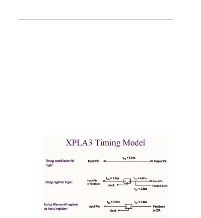
Simple Timing Model
Figure 2-26 shows the XPLA3 timing model, which has three main timing parameters: T PD , T SU , and T CO .
In other architectures, you may be able to fit the design into the CPLD, but you may not be sure whether system timing requirements can be met until after the design has been fit into the device.
This is because the timing models of other architectures are very complex including such things as timing dependencies on the number of parallel expanders borrowed, sharable expanders, and varying numbers of X and Y routing channels.
In the XPLA3 architecture, you know up-front whether the design will meet system timing requirements. This is because of the simplicity of the timing model.
FIGURE 2-26: COOLRUNNER XPLA3 SIMPLE TIMING MODEL
Xilinx • 52

XILINX SOLUTIONS
Slew Rate Control
XPLA3 devices have slew rate control for each macrocell output pin. You have the option to enable the slew rate control to reduce EMI. The nominal delay for using this option is 2.0 ns.
XPLA3 Software Tools
Software support for XPLA3 devices is provided by Xilinx WebPOWERED software products, which include the WebFITTER CPLD design fitting tool and WebPACK ISE software. Both tools are free.
In addition, EDIF input is supported for all major third-party software flows, such as Cadence Design Systems, Mentor Graphics, Viewlogic, Exemplar, and Synopsys.
TABLE 2-4: COOLRUNNER SUMMARY OF FEATURES AND BENEFITS
Features |
Benefits |
Total CMOS architecture with FZP |
Lowest stand-by current and total |
design technology |
current consumption of any CPLD; |
|
therefore longer battery life, |
|
increased reliability, and less heat |
|
dissipation |
|
|
32 to 512 macrocell device |
Suits full range of designs and |
selections |
applications; able to migrate up |
|
and down densities if design grows |
|
or shrinks |
|
|
5V tolerant I/Os and multi I/O |
Simplifies multi-voltage design |
standards |
and level shifting |
|
|
PLA array |
Optimizes sharing and resource |
|
utilization (all product terms |
|
available) |
|
|
Bus-friendly I/O |
Pull-up resistor for I/O termination |
|
|
Multiple clocking options |
Design flexibility |
|
|
Fast input registers |
Supports direct high-speed |
|
interface |
|
|
Xilinx • 53
PROGRAMMABLE LOGIC DESIGN: QUICK START HANDBOOK • CHAPTER 2
TABLE 2-4: COOLRUNNER SUMMARY OF FEATURES AND BENEFITS (CONTINUED)
|
Features |
Benefits |
|
|
|
|
|
VFM (Variable Function MUX) and |
Superior logic optimization and |
||
foldback NANDs |
device fitting – fit first time designs |
||
|
|
and lower costs by being able to use |
|
|
|
a smaller device |
|
|
|
|
|
Small, surface mount packages – |
Smallest footprint and board space |
||
0.8 mm and 0.5 mm ball pitch chip |
savings ideal for handheld devices |
||
scale packages |
like PDAs and cellphones |
||
|
|
|
|
Industrial, commercial, and |
Can be used in all application areas |
||
automotive temperature ranges |
from telematics and set-top boxes |
||
|
|
to medical and harsh environment |
|
|
|
applications |
|
|
|
|
|
|
|
|
|
|
|
|
|
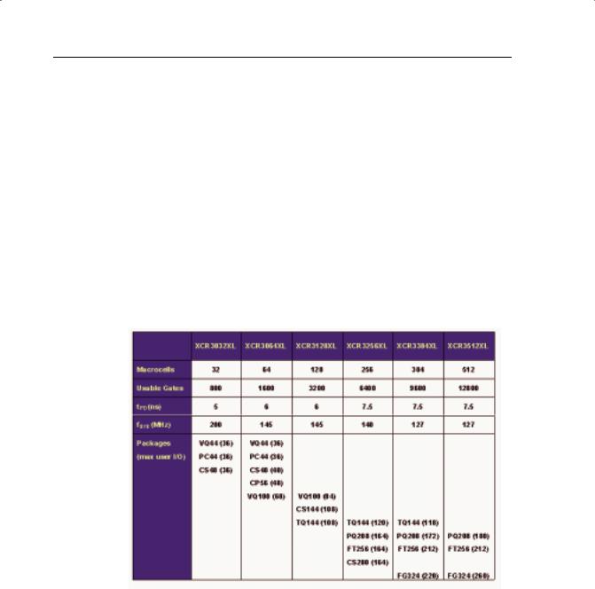
FIGURE 2-27: COOLRUNNER FAMILY OVERVIEW
Xilinx • 54