
- •Navigating This Book
- •Table of Contents
- •Introduction
- •The History of Programmable Logic
- •Complex Programmable Logic Devices (CPLDs)
- •Why Use a CPLD?
- •Field Programmable Gate Arrays (FPGAs)
- •Design Integration
- •The Basic Design Process
- •HDL File Change Example
- •Before (16 x 16 multiplier):
- •After (32 x 32 multiplier):
- •Intellectual Property (IP) Cores
- •Design Verification
- •Xilinx Solutions
- •Introduction
- •Xilinx Devices
- •Platform FPGAs
- •Virtex FPGAs
- •Virtex-II Pro FPGAs
- •Virtex FPGAs
- •Spartan FPGAs
- •Spartan-3 FPGAs
- •Spartan-IIE FPGAs
- •Spartan-IIE Architectural Features
- •Xilinx CPLDs
- •XC9500 ISP CPLD Overview
- •XC9500XL 3.3V Family
- •XC9500XV 2.5V CPLD Family
- •CoolRunner Low-Power CPLDs
- •CoolRunner-II CPLDs
- •CoolRunner Reference Designs
- •Military and Aerospace
- •Automotive and Industrial
- •Design Tools
- •Design Entry
- •Synthesis
- •Implementation and Configuration
- •Board-Level Integration
- •Verification Technologies
- •Advanced Design Techniques
- •Embedded SW Design Tools Center
- •Xilinx IP Cores
- •Web-Based Information Guide
- •End Markets
- •Silicon Products and Solutions
- •Design Resources
- •System Resources
- •Xilinx Online (IRL)
- •Configuration Solutions
- •Processor Central
- •Tools and Partnerships
- •Memory Corner
- •Silicon
- •Design Tools and Boards
- •Technical Literature and Training
- •Connectivity Central
- •High-Speed Design Resources
- •Signal Integrity Tools
- •Partnerships
- •Signal Integrity
- •Services
- •Xilinx Design Services
- •Education Services
- •Live E-Learning Environment
- •Day Segment Courses
- •Computer-Based Training (CBT)
- •University Program
- •Design Consultants
- •Technical Support
- •Module Descriptions
- •WebPACK Design Suite
- •WebPACK Design Entry
- •WebPACK StateCAD
- •WebPACK MXE Simulator
- •WebPACK HDL Bencher Tool
- •WebPACK FPGA Implementation Tools
- •WebPACK CPLD Implementation Tools
- •WebPACK iMPACT Programmer
- •WebPACK ChipViewer
- •XPower
- •WebPACK CD-ROM Installation
- •Getting Started
- •Licenses
- •Projects
- •Summary
- •Introduction
- •Design Entry
- •The Language Template
- •Close the Language Templates
- •Edit the Counter Module
- •Save the Counter Module
- •Functional Simulation
- •State Machine Editor
- •Top-Level VHDL Designs
- •Top-Level Schematic Designs
- •ECS Hints
- •I/O Markers
- •Implementing CPLDs
- •Introduction
- •Synthesis
- •Constraints Editor
- •CPLD Reports
- •Timing Simulation
- •Configuration
- •Implementing FPGAs
- •Introduction
- •Synthesis
- •The Constraints File
- •FPGA Reports
- •Programming
- •Summary
- •Design Reference Bank
- •Introduction
- •Get the Most out of Microcontroller-Based Designs
- •Conventional Stepper Motor Control
- •Using a Microcontroller to Control a Stepper Motor
- •Stepper Motor Control Using a CPLD
- •PC-Based Motor Control
- •Design Partitioning
- •Conclusion
- •Documentation and Example Code
- •Website Reference
- •ACRONYMS
- •GLOSSARY OF TERMS

CHA PT E R 1
Introduction
The History of Programmable Logic
By the late 1970s, standard logic devices were all the rage, and printed circuit boards were loaded with them. Then someone asked, “What if we gave designers the ability to implement different interconnections in a bigger device?” This would allow designers to integrate many standard logic devices into one part.
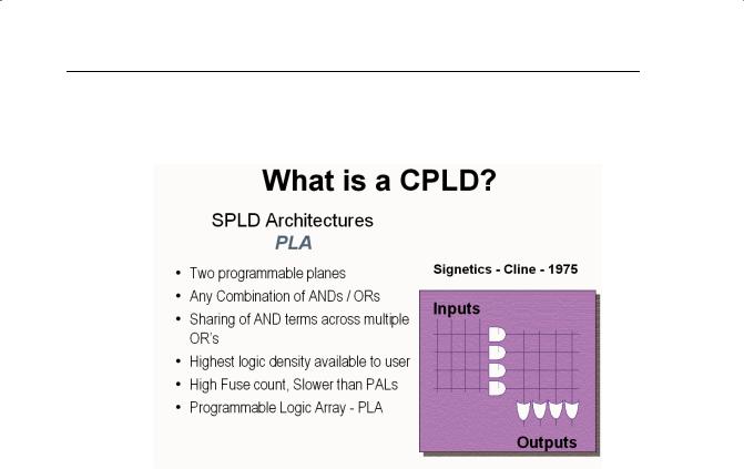
To offer the ultimate in design flexibility, Ron Cline from Signetics™ (which was later purchased by Philips and then eventually Xilinx) came up with the idea of two programmable planes. These two planes provided any combination of “AND” and “OR” gates, as well as sharing of AND terms across multiple ORs.

PROGRAMMABLE LOGIC DESIGN: QUICK START HANDBOOK • CHAPTER 1
This architecture was very flexible, but at the time wafer geometries of 10 µm made the input-to-output delay (or propagation delay) high, which made the devices relatively slow.
FIGURE 1-1: WHAT IS A CPLD?
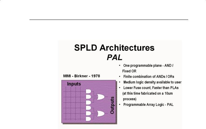
MMI (later purchased by AMD™) was enlisted as a second source for the PLA array. After fabrication issues, it was modified to become the programmable array logic (PAL) architecture by fixing one of the programmable planes.
This new architecture differed from that of the PLA in that one of the programmable planes was fixed – the OR array. PAL architecture also had the added benefit of faster Tpd and less complex software, but without the flexibility of the PLA structure.
Xilinx • 2

INTRODUCTION
Other architectures followed, such as the PLD. This category of devices is often called Simple PLD.
FIGURE 1-2: SPLD ARCHITECTURES
The architecture had a mesh of horizontal and vertical interconnect tracks. At each junction was a fuse. With the aid of software tools, designers could select which junctions would not be connected by “blowing” all unwanted fuses. (This was done by a device programmer, but more commonly these days is achieved with ISP).
Input pins were connected to the vertical interconnect. The horizontal tracks were connected to AND-OR gates, also called “product terms”. These in turn connected to dedicated flip-flops, whose outputs were connected to output pins.
PLDs provided as much as 50 times more gates in a single package than discrete logic devices! This was a huge improvement, not to mention fewer devices needed in inventory and a higher reliability over standard logic.
PLD technology has moved on from the early days with companies such as Xilinx producing ultra-low-power CMOS devices based on flash memory technology. Flash PLDs provide the ability to program the devices time and time again, electrically programming and erasing the device. Gone are the days of erasing for more than 20 minutes under an UV eraser.
Xilinx • 3