

XILINX SOLUTIONS
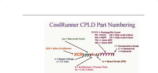
FIGURE 2-28: COOLRUNNER XPLA3 PART NUMBER SYSTEM
COOLRUNNER-II CPLDS
Xilinx CoolRunner-II CPLDs deliver the high speed and ease of use associated with the XC9500/XL/XV CPLD family and the extremely low power versatility of the XPLA3.
This means that the exact same parts can be used for high-speed data communications, computing systems, and leading-edge portable products, with the added benefit of ISP.
Low power consumption and high-speed operation are combined into a single family that is easy to use and cost effective. Xilinx-patented Fast Zero Power architecture inherently delivers extremely low power performance without the need for special design measures.
Clocking techniques and other power-saving features extend your power budget. These design features are supported from Xilinx ISE 4.1i, the WebFITTER CPLD design tool, and WebPACK ISE software onwards.
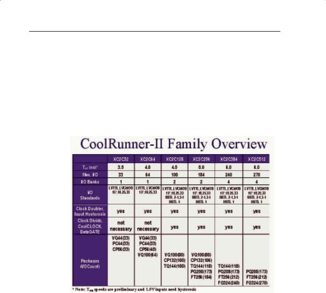
Figure 2-29 shows the CoolRunner-II CPLD package offering with corresponding I/O count. All packages are surface mount, with more than half of them ball-grid technologies. The ultra-tiny packages permit maximum functional capacity in the smallest possible area.
The CMOS technology used in CoolRunner-II CPLDs generates minimal heat, allowing the use of tiny packages during high-speed operation.
At least two densities are present in each package, with three in the VQ100 (100-pin, 1.0 mm QFP) and TQ144 (144-pin, 1.4 mm QFP), and in the FT256 (256ball, 1.0 mm-spacing FLBGA).
The FT256 is particularly suited for slim-dimensioned portable products with midto high-density logic requirements.
Xilinx • 55
PROGRAMMABLE LOGIC DESIGN: QUICK START HANDBOOK • CHAPTER 2
Figure 2-29 also details the distribution of advanced features across the CoolRunner-II CPLD family. The family has uniform basic features, with advanced features included in densities where they are most useful. For example, it is unlikely that you would need four I/O banks on 32and 64-macrocell parts, but very likely for 384and 512-macrocell parts.
The I/O banks are groupings of I/O pins using any one of a subset of compatible voltage standards that share the same V CCIO level. The clock division capability is less efficient on small parts, but more useful and likely to be used on larger ones. DataGATE™ technology, an ability to block and latch inputs to save power, is valuable in larger parts, but brings marginal benefit to small parts.
FIGURE 2-29: COOLRUNNER-II FAMILY OVERVIEW
CoolRunner-II Architecture Description
The CoolRunner-II CPLD is a highly uniform family of fast, low-power devices. The underlying architecture is a traditional CPLD architecture, combining macrocells into function blocks interconnected with a global routing matrix, the Xilinx Advanced Interconnect Matrix (AIM).
The function blocks use a PLA configuration that allows all product terms to be routed and shared among any of the macrocells of the function block.
Xilinx • 56
XILINX SOLUTIONS
Design software can efficiently synthesize and optimize logic that is subsequently fit to the function blocks and connected with the ability to utilize a very high percentage of device resources.
The software easily and automatically manages design changes, exploiting the 100% routeability of the PLA within each function block. This extremely robust building block delivers the industry’s highest pin-out retention under very broad design conditions.
The design software automatically manages device resources so that you can express your designs using completely generic constructs, without needing to know the architectural details. If you’re more experienced, you can take advantage of these details to more thoroughly understand the software’s choices and direct its results.
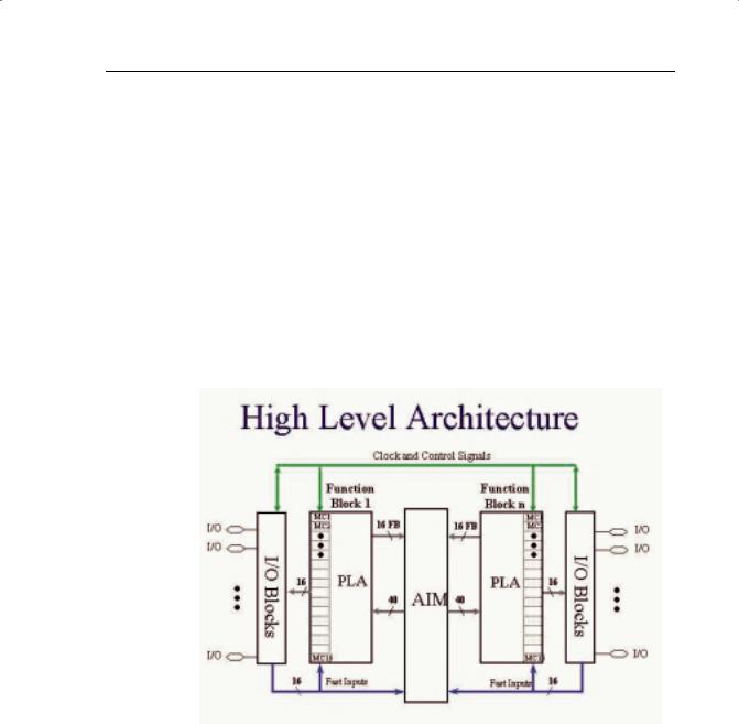
Figure 2-30 shows the high-level architecture whereby function blocks attach to pins and interconnect to each other within the internal interconnect matrix. Each function block contains 16 macrocells.
FIGURE 2-30: COOLRUNNER-II HIGH-LEVEL ARCHITECTURE
CoolRunner-II Function Block
The CoolRunner-II CPLD function blocks contain 16 macrocells, with 40 entry sites for signals to arrive for logic creation and connection.
The internal logic engine is a 56-product term PLA. All function blocks, regardless of the number contained in the device, are identical.
Xilinx • 57
PROGRAMMABLE LOGIC DESIGN: QUICK START HANDBOOK • CHAPTER 2
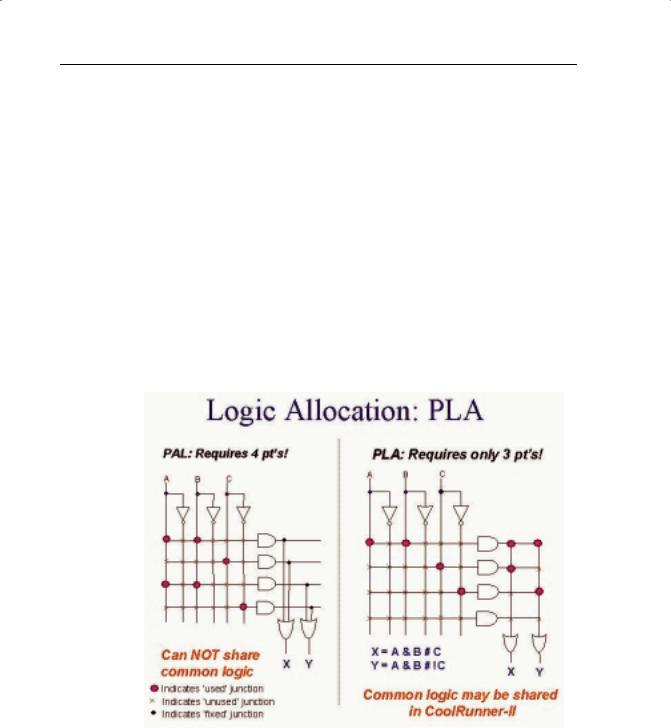
At the high level, the p-terms reside in a PLA. This structure is extremely flexible and very robust when compared to fixed or cascaded p-term function blocks.
Classic CPLDs typically have a few p-terms available for a high-speed path to a given macrocell. They rely on capturing unused p-terms from neighboring macrocells to expand their product term tally when needed.
The result of this architecture is a variable timing model and the possibility of stranding unusable logic within the function block.
The PLA is different – and better. First, any p-term can be attached to any OR gate inside the function block macrocell(s).
Second, any logic function can have as many p-terms as needed attached to it within the function block, to an upper limit of 56.
Third, you can reuse product terms at multiple macrocell OR functions so that within a function block, you need only create a particular logical product once, but you can reuse it as many as 16 times within the function block. Naturally, this works well with the fitting software, which identifies product terms that can be shared.
FIGURE 2-31: LOGIC ALLOCATION – TYPICAL PAL VS. PLA
Xilinx • 58
XILINX SOLUTIONS
The software places as many functions as it can into function blocks. There is no need to force macrocell functions to be adjacent or have any other restriction except for residing in the same function block, which is handled by the software.
Functions need not share a common clock, common set/reset, or common output enable to take full advantage of the PLA. In addition, every p-term arrives with the same time delay incurred. There are no cascade time adders for putting more product terms in the function block.
When the function block p-term budget is reached, a small interconnect timing penalty routes signals to another function block to continue creating logic. Xilinx design software handles all this automatically.
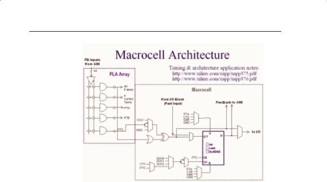
CoolRunner-II Macrocell
The CoolRunner-II CPLD macrocell is extremely efficient and streamlined for logic creation. You can develop SOP logic expressions comprising as many as 40 inputs and span 56 product terms within a single function block.
The macrocell can further combine the SOP expression into an XOR gate with another single p-term expression.
The resulting logic expression’s polarity is also selectable. The logic function can be pure combinatorial or registered, with the storage element operating selectively as a D or T flip-flop, or transparent latch.
Available at each macrocell are independent selections of global, functionblock level, or local p-term-derived clocks, sets, resets, and output enables. Each macrocell flip-flop is configurable for either single edge or DualEDGE clocking, providing either double data rate capability or the ability to distribute a slower clock (thereby saving power).
For single-edge clocking or latching, either clock polarity may be selected per macrocell.
CoolRunner-II macrocell details are shown in Figure 2-32. Standard logic symbols are used in the in figure, except the trapezoidal multiplexers have input selection from statically programmed configuration select lines (not shown).
Xilinx application note XAPP376 gives a detailed explanation of how logic is created in the CoolRunner-II CPLD family.
Xilinx • 59
PROGRAMMABLE LOGIC DESIGN: QUICK START HANDBOOK • CHAPTER 2
FIGURE 2-32: COOLRUNNER-II MACROCELL
When configured as a D-type flip-flop, each macrocell has an optional clock enable signal permitting state hold while a clock runs freely.
Note that control terms are available to be shared for key functions within the function block, and are generally used whenever the exact same logic function would be repeatedly created at multiple macrocells.
The control term product terms are available for function block clocking (CTC), function block asynchronous set (CTS), function block asynchronous reset (CTR), and function block output enable (CTE).
You can configure any macrocell flip-flop as an input register or latch, which takes in the signal from the macrocell’s I/O pin and directly drives the AIM. The macrocell combinatorial functionality is retained for use as a buried logic node if needed.
Advanced Interconnect Matrix (AIM)
AIM is a highly connected low-power rapid switch directed by the software to deliver a set of as many as 40 signals to each function block for the creation of logic.
Results from all function block macrocells, as well as all pin inputs, circulate back through the AIM for additional connection available to all other function blocks, as dictated by the design software. The AIM minimizes both propagation delay and power as it makes attachments to the various function blocks.
Xilinx • 60
XILINX SOLUTIONS
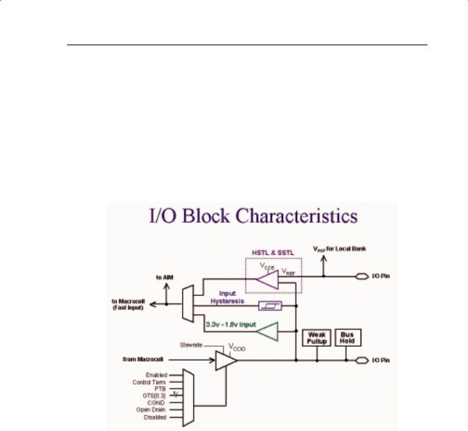
I/O Blocks
I/O blocks are primarily transceivers. However, each I/O is either automatically compliant with standard voltage ranges or can be programmed to become compliant.
In addition to voltage levels, each input can selectively arrive through Schmitt-trigger inputs. This adds a small time delay, but substantially reduces noise on that input pin.
Hysteresis also allows easy generation of external clock circuits. The Schmitt-trigger path is best illustrated in Figure 2-33. Outputs can be directly driven, tri-stated, or open-drain configured. A choice of slow or fast slew rate output signal is also available.
FIGURE 2-33: COOLRUNNER-II I/O BLOCK
Output Banking
CPLDs are widely used as voltage interface translators; thus, the output pins are grouped in large banks.
The smallest parts are not banked, so all signals will have the same output swing for 32and 64-macrocell parts.
The medium parts (128 and 256 macrocell) support two output banks. With two, the outputs will switch to one of two selected output voltage levels, unless both banks are set to the same voltage.
Xilinx • 61
PROGRAMMABLE LOGIC DESIGN: QUICK START HANDBOOK • CHAPTER 2
The larger parts (384 and 512 macrocell) support four output banks, split evenly. They can support groupings of one, two, three, or four separate output voltage levels. This kind of flexibility permits easy interfacing to 3.3V, 2.5V, 1.8V, and 1.5V in a single part.
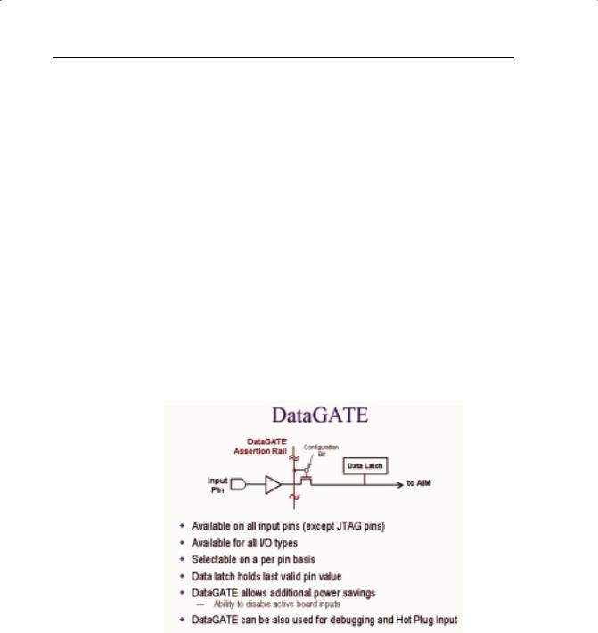
DataGATE
Low power is the hallmark of CMOS technology. Other CPLD families use a sense amplifier approach to create p-terms, which always has a residual current component.
This residual current can be several hundred milliamps, making these CPLDs unusable in portable systems.
CoolRunner-II CPLDs use standard CMOS methods to create the CPLD architecture and deliver the corresponding low current consumption, without any special tricks.
However, sometimes you might want to reduce the system current even more by selectively disabling unused circuitry. The patented DataGATE technology permits a straightforward approach to additional power reduction.
Each I/O pin has a series switch that can block the arrival of unused freerunning signals that may increase power consumption. Disabling these switches enables you to complete your design and choose which sections will participate in the DataGATE function.
FIGURE 2-34: DATAGATE FUNCTION IN COOLRUNNER-II CPLDS
The DataGATE logic function drives an assertion rail threaded through mediumand high-density CoolRunner-II CPLD parts.
Xilinx • 62

XILINX SOLUTIONS
You can select which inputs to block under the control of the DataGATE function, effectively blocking controlled switching signals so that they do not drive internal chip capacitances.
Output signals that do not switch are held by the bus hold feature. You can choose any set of input pins can be chosen to participate in the DataGATE function.
Figure 2-34 shows how DataGATE function works. One I/O pin drives the DataGATE assertion rail. It can have any desired logic function on it – something as simple as mapping an input pin to the DataGATE function or as complex as a counter or state machine output driving the DataGATE I/O pin through a macrocell.
When the DataGATE rail is asserted low, any pass transistor switch attached to it is blocked. Each pin has the ability to attach to the AIM through a DataGATE pass transistor, and be blocked.
A latch automatically captures the state of the pin when it becomes blocked. The DataGATE assertion rail threads throughout all possible I/Os, so each can participate if chosen.
One macrocell is singled out to drive the rail, and that macrocell is exposed to the outside world (through a pin) for inspection. If the DataGATE function is not needed, this pin is an ordinary I/O.
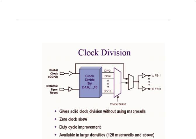
Additional Clock Options: Division, DualEDGE, and CoolCLOCK
Division
Circuitry has been included in the CoolRunner-II CPLD architecture to divide one externally supplied global clock by standard values, with options for division by 2, 4, 6, 8, 10, 12, 14, and 16 (see Figure 2-35). This capability is supplied on the GCK2 pin.
The resulting clock produced will be 50% duty cycle for all possible divisions.
Xilinx • 63
PROGRAMMABLE LOGIC DESIGN: QUICK START HANDBOOK • CHAPTER 2
Note that a synchronous reset is included to guarantee that no runt clocks can get through to the global clock nets. The signal is buffered and driven to multiple traces with minimal loading and skew.
FIGURE 2-35: COOLRUNNER-II CLOCK DIVISION
DualEDGE
Each macrocell has the ability to double its input clock switching frequency. Figure 2-32 shows the macrocell flip-flop with the DualEDGE option (doubled clock) at each macrocell.
The source to double can be a control term clock, a product term clock, or one of the available global clocks. The ability to switch on both clock edges is vital for a number of synchronous memory interface applications as well as certain double data rate I/O applications.
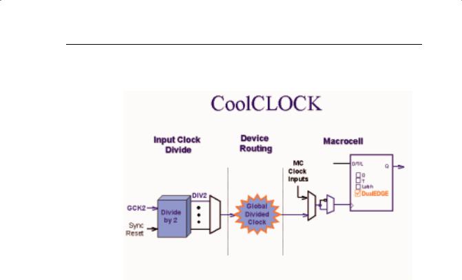
CoolCLOCK
In addition to the DualEDGE flip-flop, you can gain additional power savings by combining the clock division circuitry with the DualEDGE circuitry. This capability is called CoolCLOCK and is designed to reduce clocking power within the CPLD.
Because the clock net can be a significant power drain, you can reduce the clock power by driving the net at half frequency, and then doubling the clock rate using DualEDGE triggering at the macrocells.
Xilinx • 64
XILINX SOLUTIONS
Figure 2-36 illustrates how CoolCLOCK is created by internal clock cascading, with the divider and DualEDGE flip-flop working together.
FIGURE 2-36: COOLCLOCK
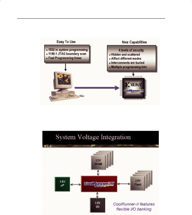
Design Security
You can secure your designs during programming to prevent either accidental overwriting or pattern theft via readback.
CoolRunner-II CPLDs have four independent levels of security provided on-chip, eliminating any electrical or visual detection of configuration patterns.
Xilinx • 65
PROGRAMMABLE LOGIC DESIGN: QUICK START HANDBOOK • CHAPTER 2
These security bits can be reset only by erasing the entire device. Additional details are omitted intentionally.
FIGURE 2-37: COOLRUNNER-II DEVICE SECURITY
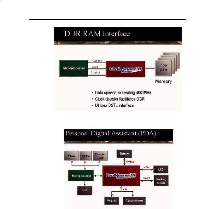
CoolRunner-II Application Examples
FIGURE 2-38: SYSTEM VOLTAFE INTEGRATION EXAMPLE
Xilinx • 66
XILINX SOLUTIONS
FIGURE 2-39: DDR RAM INTERFACE EXAMPLE
FIGURE 2-40: PDA USING FREE REFERENCE DESIGNS EXAMPLE
Xilinx • 67