

Fundamentals of Microelectronics
.pdfBR |
Wiley/Razavi/Fundamentals of Microelectronics [Razavi.cls v. 2006] |
June 30, 2007 at 13:42 |
81 (1) |
|
|
|
|
Sec. 3.4 |
Large-Signal and Small-Signal Operation |
81 |
|
= 3VT ln IX |
(3.39) |
|
IS |
|
|
= 2:412 V: |
(3.40) |
This value of Vout gives a new value for IX : |
|
|
|
IX = Vad , Vout |
(3.41) |
|
R1 |
|
|
= 6:88 mA; |
(3.42) |
which translates to a new Vout: |
|
|
|
Vout = 3VD |
(3.43) |
|
= 2:411 V: |
(3.44) |
Noting the very small difference between (3.40) and (3.44), we conclude that Vout |
= 2:411 V |
|
with good accuracy. The constant-voltage diode model would not be useful in this case.
Exercise
Repeat the above example if an output voltage of 2.35 is desired.
The situation described above is an example of small “perturbations” in circuits. The change in Vad from 3 V to 3.1 V results in a small change in the circuit's voltages and currents, motivating us to seek a simpler analysis method that can replace the nonlinear equations and the inevitable iterative procedure. Of course, since the above example does not present an overwhelmingly difficult problem, the reader may wonder if a simpler approach is really necessary. But, as seen in subsequent chapters, circuits containing complex devices such as transistors may indeed become impossible to analyze if the nonlinear equations are retained.
These thoughts lead us to the extremely important concept of “small-signal operation,” whereby the circuit experiences only small changes in voltages and currents and can therefore be simplified through the use of “small-signal models” for nonlinear devices. The simplicity arises because such models are linear, allowing standard circuit analysis and obviating the need for iteration. The definition of “small” will become clear later.
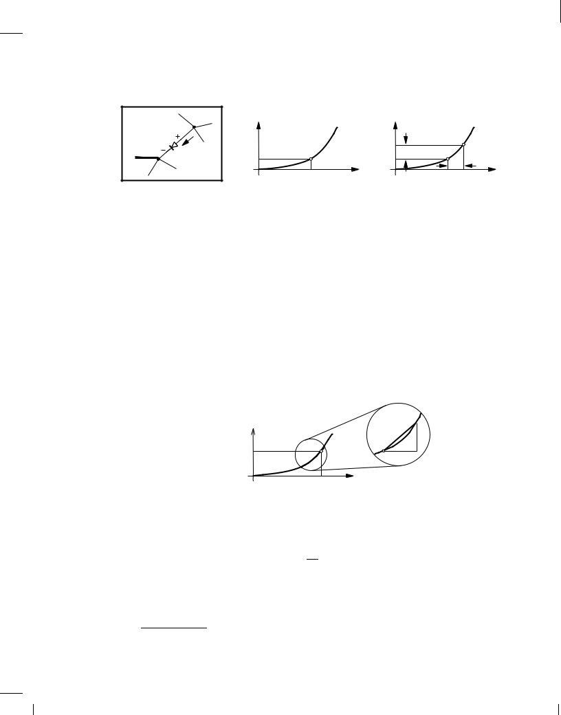
To develop our understanding of small-signal operation, let us consider diode D1 in Fig. 3.20(a), which sustains a voltage VD1 and carries a current ID1 [point A in Fig. 3.20(b)]. Now suppose a perturbation in the circuit changes the diode voltage by a small amount VD [point B in Fig. 3.20(c)]. How do we predict the change in the diode current, ID? We can begin with the nonlinear characteristic:
|
|
I |
= I |
S |
exp VD1 |
+ V |
|
(3.45) |
||||
|
|
D2 |
|
|
|
|
VT |
|
|
|
|
|
|
|
|
|
|
|
|
|
|
|
|
|
|
|
|
|
= IS exp |
VD1 |
exp |
V : |
|
(3.46) |
||||
|
|
|
|
|
|
|
VT |
|
|
VT |
|
|
If V VT , then exp( V=VT ) 1 + V=VT and |
|
|
|
|
||||||||
I |
|
= I |
|
exp |
VD1 + V I |
|
exp |
VD1 |
(3.47) |
|||
|
D2 |
S |
|
|
VT |
VT S |
|
VT |
|
|||
BR |
Wiley/Razavi/Fundamentals of Microelectronics [Razavi.cls v. 2006] |
June 30, 2007 at 13:42 |
82 (1) |
|
|
|
|
82 |
Chap. 3 |
Diode Models and Circuits |
|
I D |
|
I D |
|
|
|
VD1 |
I D1 |
|
I D2 |
B |
|
|
D1 |
|
A |
|
|
||
A |
|
? |
V |
|
||
|
I D1 |
|
I D1 |
|
D |
|
|
|
|
|
|
|
|
|
VD1 |
VD |
|
VD1 VD2 |
|
VD |
(a) |
(b) |
|
|
(c) |
|
|
Figure 3.20 (a) General circuit containing a diode, (b) operating point of D1, (c) change in ID as a result of change in VD.
= ID1 + |
V ID1: |
|
(3.48) |
||
|
VT |
|
|
|
|
That is, |
|
|
|
|
|
I |
|
= |
V I |
: |
(3.49) |
|
D |
|
VT D1 |
|
|
The key observation here is that ID is a linear function of V , with a proportionality factor equal to ID1=VT . (Note that larger values of ID1 lead to a greater ID for a given VD. The significance of this trend becomes clear later.)
The above result should not come as a surprise: if the change in VD is small, the section of the characteristic in Fig. 3.20(c) between points A and B can be approximated by a straight line (Fig. 3.21), with a slope equal to the local slope of the characteristic. In other words,
I D 
B
I D2
A
I D1 
VD1 VD2 VD
Figure 3.21 Approximation of characteristic by a straight line.
ID = dID jV D=V D1
VD dVD
= IS exp VD1
VT VT
= ID1 ;
VT
which yields the same result as that in Eq. (3.49).8
I D2  B
B
I D
I D1
A VD
(3.50)
(3.51)
(3.52)
8This is also to be expected. Writing Eq. (3.45) to obtain the change in ID for a small change in VD is in fact equivalent to taking the derivative.

BR |
Wiley/Razavi/Fundamentals of Microelectronics [Razavi.cls v. 2006] |
June 30, 2007 at 13:42 |
83 (1) |
|
|
|
|
Sec. 3.4 |
Large-Signal and Small-Signal Operation |
83 |
Let us summarize our results thus far. If the voltage across a diode changes by a small amount (much less than VT ), then the change in the current is given by Eq. (3.49). Equivalently, for small-signal analysis, we can assume the operation is at a point such as A in Fig. 3.21 and, due to a small perturbation, it moves on a straight line to point B with a slope equal to the local slope of the characteristic (i.e., dID=dVD calculated at VD = VD1 or ID = ID1). Point A is called the “bias” point or the “operating” point. 9
Example 3.18
A diode is biased at a current of 1 mA. (a) Determine the current change if VD changes by 1 mV.
(b) Determine the voltage change if ID changes by 10%.
Solution
(a) We have |
|
|
|
|
|
|
|
|
I |
= ID V |
D |
(3.53) |
|
|
|
D |
VT |
|
||
|
|
|
|
|
||
|
|
|
= 38:4 A: |
(3.54) |
||
(b) Using the same equation yields |
|
|
|
|
|
|
V |
D |
= VT I |
|
|
(3.55) |
|
|
ID |
D |
|
|
|
|
|
|
|
|
|
|
|
|
|
= 26 mV |
(0:1 mA) |
(3.56) |
||
|
|
1 mA |
|
|
|
|
|
|
= 2:6 mV: |
|
|
(3.57) |
|
Exercise
In response to a current change of 1 mA, a diode exhibits a voltage change of 3 mV. Calculate the bias current of the diode.
Equation (3.55) in the above example reveals an interesting aspect of small-signal operation: as far as (small) changes in the diode current and voltage are concerned, the device behaves as a linear resistor. In analogy with Ohm's Law, we define the “small-signal resistance” of the diode as:
r = VT : |
(3.58) |
d ID
This quantity is also called the “incremental” resistance to emphasize its validity for small changes. In the above example, rd = 26 .
Figure 3.22(a) summarizes the results of our derivations for a forward-biased diode. For bias calculations, the diode is replaced with an ideal voltage source of value VD;on, and for small changes, with a resistance equal to rd. For example, the circuit of Fig. 3.22(b) is transformed to that in Fig. 3.22(c) if only small changes in V1 and Vout are of interest. Note that v1 and vout in
9Also called the “quiescent” point.
BR |
Wiley/Razavi/Fundamentals of Microelectronics [Razavi.cls v. 2006] |
June 30, 2007 at 13:42 |
84 (1) |
|
|
|
|
84 |
Chap. 3 |
Diode Models and Circuits |
Fig. 3.22(c) represent changes in voltage and are called small-signal quantities. In general, we denote small-signal voltages and currents by lower-case letters.
|
|
|
R1 |
|
|
R1 |
|
VD,on |
r d |
V1 |
D1 |
Vout |
v 1 |
r d |
v out |
|
|||||||
|
|
||||||
Bias |
Small−Signal |
|
|
|
|
|
|
Model |
Model |
|
|
|
|
|
|
(a) |
|
|
(b) |
|
|
(c) |
|
Figure 3.22 Summary of diode models for bias and signal calculations, (b) circuit example, (c) smallsignal model.
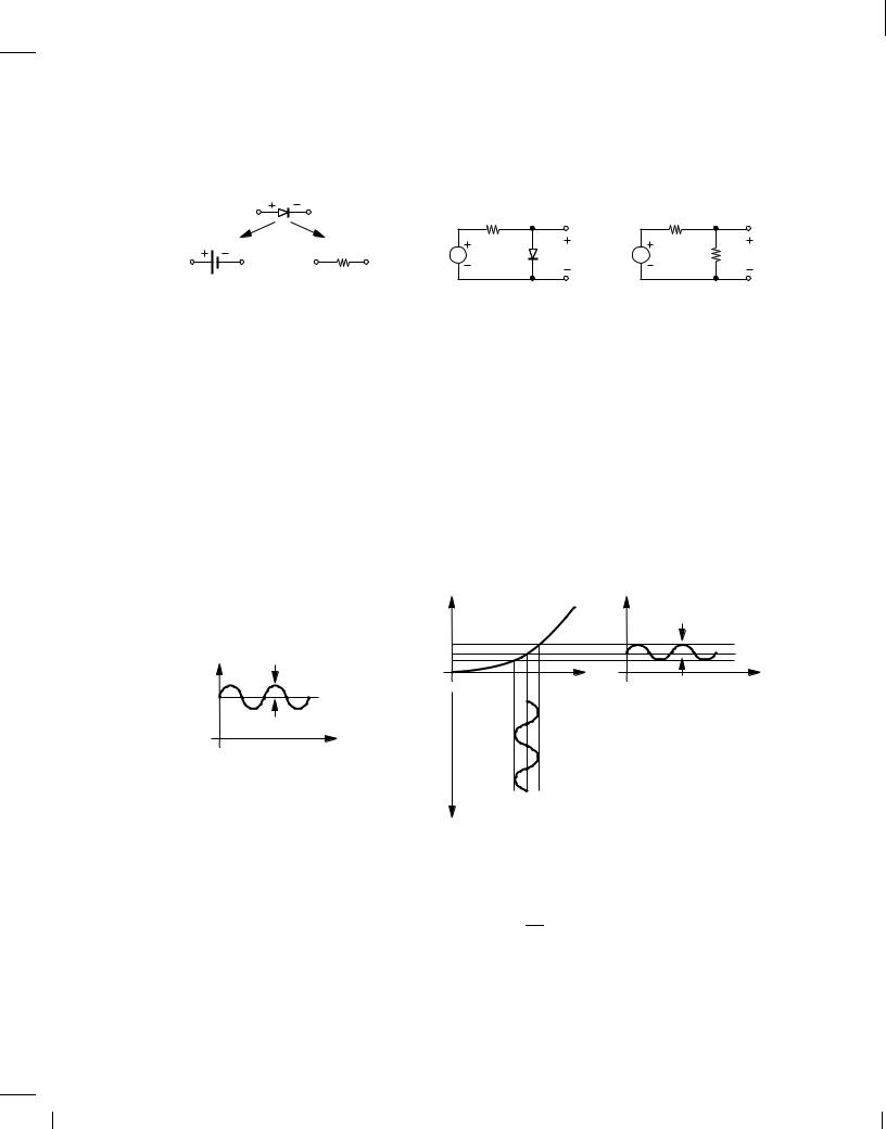
Example 3.19
A sinusoidal signal having a peak amplitude of Vp and a dc value of V0 can be expressed as V (t) = V0 + Vp cos !t. If this signal is applied across a diode and Vp VT , determine the resulting diode current.
Solution
The signal waveform is illustrated in Fig. 3.23(a). As shown in Fig. 3.23(b), we rotate this diagram by 90 so that its vertical axis is aligned with the voltage axis of the diode characteristic. With a signal swing much less than VT , we can view V0 and the corresponding current, I0, as the bias point of the diode and Vp as a small perturbation. It follows that,
|
I D |
I D |
|
|
|
|
I p |
V (t ) |
I |
0 |
|
Vp |
|
|
|
|
|
|
|
V0 |
|
|
VD |
|
|
|
|
|
t |
|
|
|
t |
|
V |
|
|
0 |
|
|
(a) |
|
(b) |
Figure 3.23 (a) Sinusoidal input along with a dc level, (b) response of a diode to the sinusoid.
I0 = IS exp V0 ;
VT
and
t
(3.59)
rd = |
VT : |
(3.60) |
|
I0 |
|

BR |
Wiley/Razavi/Fundamentals of Microelectronics [Razavi.cls v. 2006] |
June 30, 2007 at 13:42 |
85 (1) |
|
|
|
|
Sec. 3.4 Large-Signal and Small-Signal Operation 85
Thus, the peak current is simply equal to |
|
|
|
|
|
|
|
|
|
|
|
|
Ip = Vp=rd |
|
(3.61) |
||||||
|
|
= |
I0 |
V ; |
|
(3.62) |
||||
|
|
|
|
|
||||||
|
|
|
|
VT |
p |
|
|
|||
yielding |
|
|
|
|
|
|
|
|
|
|
ID(t) = I0 + Ip cos !t |
|
(3.63) |
||||||||
= I |
|
exp |
V0 |
+ |
|
I0 |
V cos !t: |
(3.64) |
||
|
|
|
||||||||
|
S |
|
VT |
|
VT |
p |
|
|||
Exercise
The diode in the above example produces a peak current of 0.1 mA in response to V0 = 800 mV and Vp = 1:5 mV. Calculate IS.
The above example demonstrates the utility of small-signal analysis. If Vp were large, we would need to solve the following equation
I (t) = I |
S |
exp V0 + Vp cos !t |
; |
(3.65) |
D |
VT |
|
|
|
|
|
|
|
a task much more difficult than the above linear calculations. 10
Example 3.20 
In the derivation leading to Eq. (3.49), we assumed a small change in VD and obtained the resulting change in ID. Beginning with VD = VT ln(ID =Is), investigate the reverse case, i.e., ID changes by a small amount and we wish to compute the change in VD.
Solution
Denoting the change in VD by VD, we have |
|
|
||||
V |
D1 |
+ V |
= V |
ln ID1 + ID |
(3.66) |
|
|
D |
T |
IS |
|
|
|
|
|
|
|
|
|
|
|
|
|
= V |
ln ID1 1 + ID |
(3.67) |
|
|
|
|
T |
IS |
ID1 |
|
|
|
|
|
|
||
|
|
|
= V |
ln ID1 + V |
ln 1 + ID : |
(3.68) |
|
|
|
T |
T |
ID1 |
|
|
|
|
|
IS |
|
|
For small-signal operation, we assume ID ID1 and note that ln(1 + ) if 1. Thus,
V |
D |
= V ID |
; |
(3.69) |
|
|
T |
ID1 |
|
|
|
|
|
|
|
|
|
which is the same as Eq. (3.49). Figure 3.24 illustrates the two cases, distinguishing between the cause and the effect.
10The function exp(a sin bt) can be approximated by a Taylor expansion or Bessel functions.
BR |
Wiley/Razavi/Fundamentals of Microelectronics [Razavi.cls v. 2006] |
June 30, 2007 at 13:42 |
86 (1) |
|
|
|
|
86 |
|
|
|
|
|
|
|
|
|
|
Chap. 3 |
|
|
Diode Models and Circuits |
||||||||
|
|
|
|
|
I D |
|
|
|
|
|
|
|
|
|
|
|
|
|
|
|
|
|
VD |
|
|
|
I D = |
VD |
|
I D |
|
|
|
|
|
|
|
|
VD |
|
VD = I D r d |
||||
|
|
|
|
|
|
|
|
|
|
|
|
|
||||||||||
|
D1 |
|
r d |
|
|
|
D1 |
|
|
|
|
|
|
|||||||||
|
|
|
|
|
|
|
|
|
|
|
|
|
|
|
|
|
VT |
|||||
|
|
= |
VD |
I D1 |
|
|
|
|
|
|
|
|
|
|
|
= I D |
||||||
|
|
|
|
|
|
|
|
|
|
|
|
|
||||||||||
|
|
V |
T |
|
|
|
|
|
|
|
|
|
|
|
I D1 |
|||||||
|
|
|
|
(a) |
|
|
|
|
|
|
|
|
|
(b) |
||||||||
|
|
|
|
|
|
|
|
|
|
|
|
|
|
|
||||||||
Figure 3.24 Change in diode current (voltage) due to a change in voltage (current).
Exercise
Repeat the above example by taking the derivative of the diode voltage equation with respect to
ID.
With our understanding of small-signal operation, we now revisit Example 3.17.
Example 3.21
Repeat part (b) of Example 3.17 with the aid of a small-signal model for the diodes.
Solution
Since each diode carries ID1 = 6 mA with an adaptor voltage of 3 V and VD1 = 800 mV, we can construct the small-signal model shown in Fig. 3.25, where vad = 100 mV and rd = (26 mV)=(6 mA) = 4:33 . (As mentioned earlier, the voltages shown in this model denote small changes.) We can thus write:
R1
v ad
Figure 3.25 Small-signal model of adaptor.
r d |
|
r d |
v out |
r d |
|
|
|
3rd |
(3.70) |
|
vout = |
|
|
vad |
|
|
R1 + 3rd |
|||
= |
11:5 mV: |
(3.71) |
||
That is, a 100-mV change in Vad yields an 11.5-mV change in Vout. In Example 3.17, solution of nonlinear diode equations predicted an 11-mV change in Vout. The small-signal analysis therefore offers reasonable accuracy while requiring much less computational effort.
Exercise
Repeat Examples (3.17) and (3.21) if the value of R1 in Fig. 3.19 is changed to 200 .
BR |
Wiley/Razavi/Fundamentals of Microelectronics [Razavi.cls v. 2006] |
June 30, 2007 at 13:42 |
87 (1) |
|
|
|
|
Sec. 3.4 |
Large-Signal and Small-Signal Operation |
87 |
Considering the power of today's computer software tools, the reader may wonder if the smallsignal model is really necessary. Indeed, we utilize sophisticated simulation tools in the design of integrated circuits today, but the intuition gained by hand analysis of a circuit proves invaluable in understanding fundamental limitations and various trade-offs that eventually lead to a compromise in the design. A good circuit designer analyzes and understands the circuit before giving it to the computer for a more accurate analysis. A bad circuit designer, on the other hand, allows the computer to think for him/her.
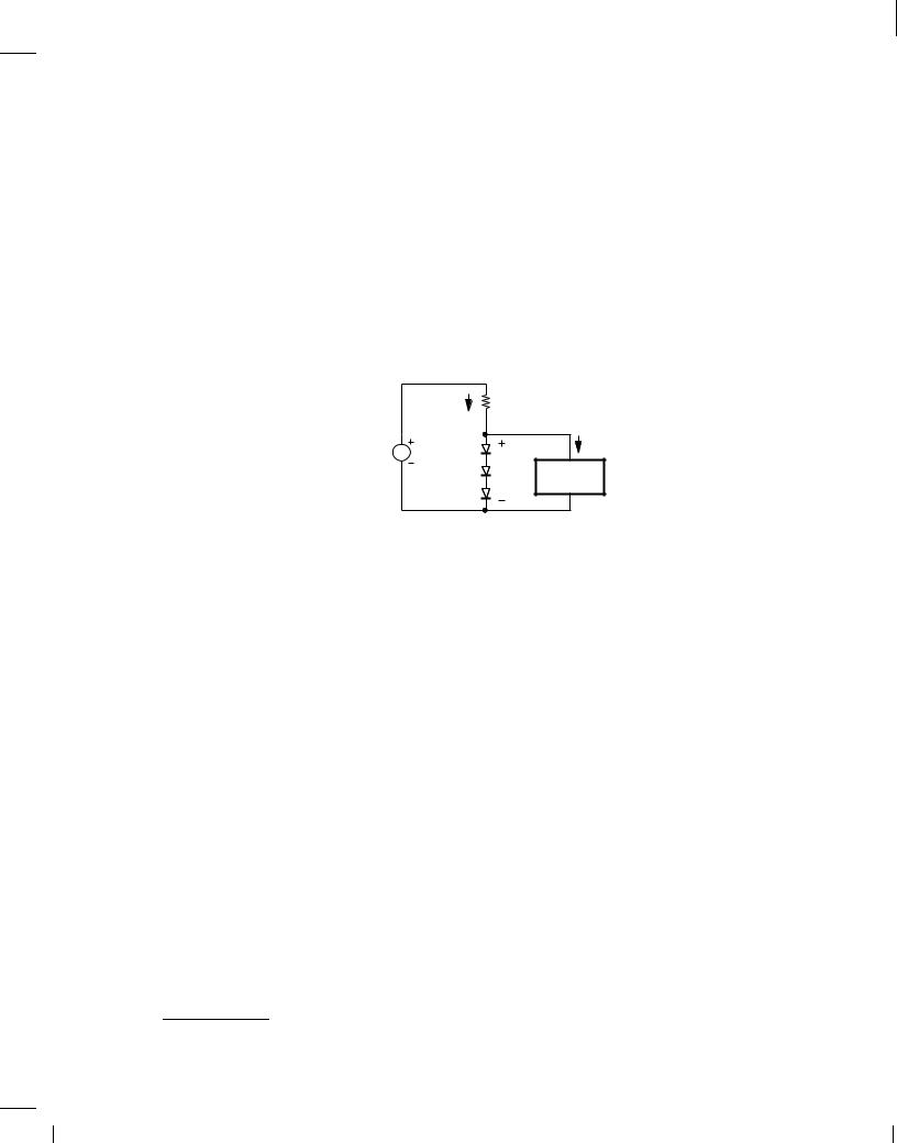
Example 3.22 
In Examples 3.17 and 3.21, the current drawn by the cellphone is neglected. Now suppose, as shown in Fig. 3.26, the load pulls a current of 0.5 mA11 and determine Vout.
~6 mA |
R1 = 100 Ω |
Vad |
0.5 mA |
|
|
|
Vout Cellphone |
Figure 3.26 Adaptor feeding a cellphone.
Solution
Since the current flowing through the diodes decreases by 0.5 mA and since this change is much less than the bias current (6 mA), we write the change in the output voltage as:
Vout = ID (3rd) |
(3.72) |
= 0:5 mA(3 4:33 ) |
(3.73) |
= 6:5 mV: |
(3.74) |
Exercise
Repeat the above example if R1 is reduced to 80 .
In summary, the analysis of circuits containing diodes (and other nonlinear devices such as transistors) proceeds in three steps: (1) determine—perhaps with the aid of the constant-voltage model— the initial values of voltages and currents (before an input change is applied); (2) develop the small-signal model for each diode (i.e., calculate rd); (3) replace each diode with its small-signal model and compute the effect of the input change.
11A cellphone in reality draws a much higher current.
BR |
Wiley/Razavi/Fundamentals of Microelectronics [Razavi.cls v. 2006] |
June 30, 2007 at 13:42 |
88 (1) |
|
|
|
|
88 |
Chap. 3 |
Diode Models and Circuits |
3.5 Applications of Diodes
The remainder of this chapter deals with circuit applications of diodes. A brief outline is shown below.
|
|
|
|
|
|
|
|
|
|
|
|
|
Half−Wave and |
|
|
Limiting |
|
|
Voltage |
|
|
Level Shifters |
|
|
Full−Wave rectifiers |
|
|
Circuits |
|
|
Doublers |
|
|
and Switches |
|
|
|
|
|
|
|
|
|
|
|
|
|
Figure 3.27 Applications of diodes.
3.5.1 Half-Wave and Full-Wave Rectifiers
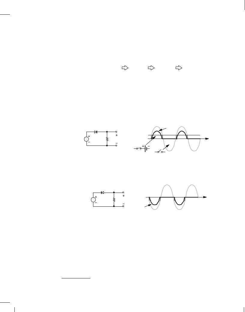
Half-Wave Rectifier Let us return to the rectifier circuit of Fig. 3.10(b) and study it more closely. In particular, we no longer assume D1 is ideal, but use a constant-voltage model. As illustrated in Fig. 3.28, Vout remains equal to zero until Vin exceeds VD;on, at which point D1 turns on and Vout = Vin , VD;on. For Vin < VD;on, D1 is off12 and Vout = 0. Thus, the circuit still operates as a rectifier but produces a slightly lower dc level.
|
D 1 |
Vin |
Vout |
Vin |
|
VD,on |
|
R 1 |
Vout |
t |
|
|
|
|
VD,on
Figure 3.28 Simple rectifier.
Example 3.23
Prove that the circuit shown in Fig. 3.29(a) is also a rectifier.
|
D 1 |
|
Vin |
|
|
|
|
Vin |
R 1 |
Vout |
t |
|
|
|
Vout |
|
(a) |
|
(b) |
Figure 3.29 Rectification of positive cycles.
Solution
In this case, D1 remains on for negative values of Vin, specifically, for Vin ,VD;on. As Vin exceeds ,VD;on, D1 turns off, allowing R2 to maintain Vout = 0. Depicted in Fig. 3.29, the resulting output reveals that this circuit is also a rectifier, but it blocks the positive cycles.
Exercise
Plot the output if D1 is an ideal diode.
12If Vin < 0, D1 carries a small leakage current, but the effect is negligible.
BR |
Wiley/Razavi/Fundamentals of Microelectronics [Razavi.cls v. 2006] |
June 30, 2007 at 13:42 |
89 (1) |
|
|
|
|
Sec. 3.5 |
Applications of Diodes |
89 |
Called a “half-wave rectifier,” the circuit of Fig. 3.28 does not produce a useful output. Unlike a battery, the rectifier generates an output that varies considerably with time and cannot supply power to electronic devices. We must therefore attempt to create a constant output.
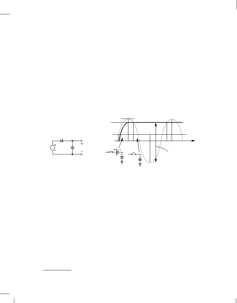
Fortunately, a simple modification solves the problem. As depicted in Fig. 3.30(a), the resistor is replaced with a capacitor. The operation of this circuit is quite different from that of the above rectifier. Assuming a constant-voltage model for D1 in forward bias, we begin with a zero initial condition across C1 and study the behavior of the circuit [Fig. 3.30(b)]. As Vin rises from zero, D1 is off until Vin > VD;on, at which point D1 begins to act as a battery and Vout = Vin ,VD;on. Thus, Vout reaches a peak value of Vp , VD;on. What happens as Vin passes its peak value? At t = t1, we have Vin = Vp and Vout = Vp , VD;on. As Vin begins to fall, Vout must remain constant. This is because if Vout were to fall, then C1 would need to be discharged by a current flowing from its top plate through the cathode of D1, which is impossible.13 The diode therefore turns off after t1. At t = t2, Vin = Vp , VD;on = Vout, i.e., the diode sustains a zero voltage difference. At t > t2, Vin < Vout and the diode experiences a negative voltage.
|
|
Vp |
Vout |
|
|
|
|
Vp − VD,on |
|
|
|
|
|
Vin |
|
|
|
|
D 1 |
VD,on |
|
|
|
|
|
|
|
|
|
Vin |
|
t 1 t 2 |
t 3 |
t 4 t 5 |
t |
C1 |
Vout |
|
|
|
Maximum
Reverse
Voltage
(a) |
(b) |
Figure 3.30 (a) Diode-capacitor circuit, (b) input and output waveforms.
Continuing our analysis, we note that at t = t3, Vin = ,Vp, applying a maximum reverse bias of Vout ,Vin = 2Vp ,VD;on across the diode. For this reason, diodes used in rectifiers must withstand a reverse voltage of approximately 2Vp with no breakdown.
Does Vout change after t = t1? Let us consider t = t4 as a potentially interesting point. Here, Vin just exceeds Vout but still cannot turn D1 on. At t = t5, Vin = Vp = Vout + VD;on, and D1 is on, but Vout exhibits no tendency to change because the situation is identical to that at t = t1. In other words, Vout remains equal to Vp , VD;on indefinitely.
Example 3.24
Assuming an ideal diode model, (a) Repeat the above analysis. (b) Plot the voltage across D1, VD1, as a function of time.
Solution
(a) With a zero initial condition across C1, D1 turns on as Vin exceeds zero and Vout = Vin. After t = t1, Vin falls below Vout, turning D1 off. Figure 3.31(a) shows the input and output waveforms.
(b) The voltage across the diode is VD1 = Vin , Vout. Using the plots in Fig. 3.31(a), we readily arrive at the waveform in Fig. 3.31(b). Interestingly, VD1 is similar to Vin but with the
13The water pipe analogy in Fig. 3.3(c) proves useful here.
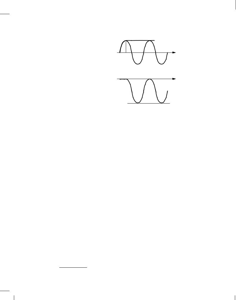
BR |
Wiley/Razavi/Fundamentals of Microelectronics [Razavi.cls v. 2006] |
June 30, 2007 at 13:42 |
90 (1) |
|
|
|
|
90 |
Chap. 3 |
Diode Models and Circuits |
|
Vout |
|
t 1 |
|
t |
|
Vin |
|
(a)
t 1
t
VD1
−2 Vp
(b)
Figure 3.31 (a) Input and output waveforms of the circuit in Fig. 3.30 with an ideal diode, (b) voltage across the diode.
average value shifted from zero to ,Vp. We will exploit this result in the design of voltage doublers (Section 3.5.4).
Exercise
Repeat the above example if the terminals of the diode are swapped.
The circuit of Fig. 3.30(a) achieves the properties required of an “ac-dc converter,” generating a constant output equal to the peak value of the input sinusoid.14 But how is the value of C1 chosen? To answer this question, we consider a more realistic application where this circuit must provide a current to a load.
Example 3.25
A laptop computer consumes an average power of 25 W with a supply voltage of 3.3 V. Determine the average current drawn from the batteries or the adapter.
Solution
Since P = V I, we have I 7:58 A. If the laptop is modeled by a resistor, RL, then RL =
V=I = 0:436 .
Exercise
What power dissipation does a 1- load represent for such a supply voltage?
14This circuit is also called a “peak detector.”