

Fundamentals of Microelectronics
.pdfBR |
Wiley/Razavi/Fundamentals of Microelectronics [Razavi.cls v. 2006] |
June 30, 2007 at 13:42 |
221 (1) |
|
|
|
|
Sec. 5.3 |
Bipolar Amplifier Topologies |
221 |
Exercise
Does the circuit operate better if RB is halved?
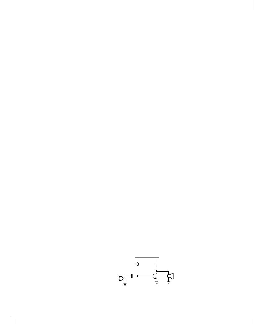
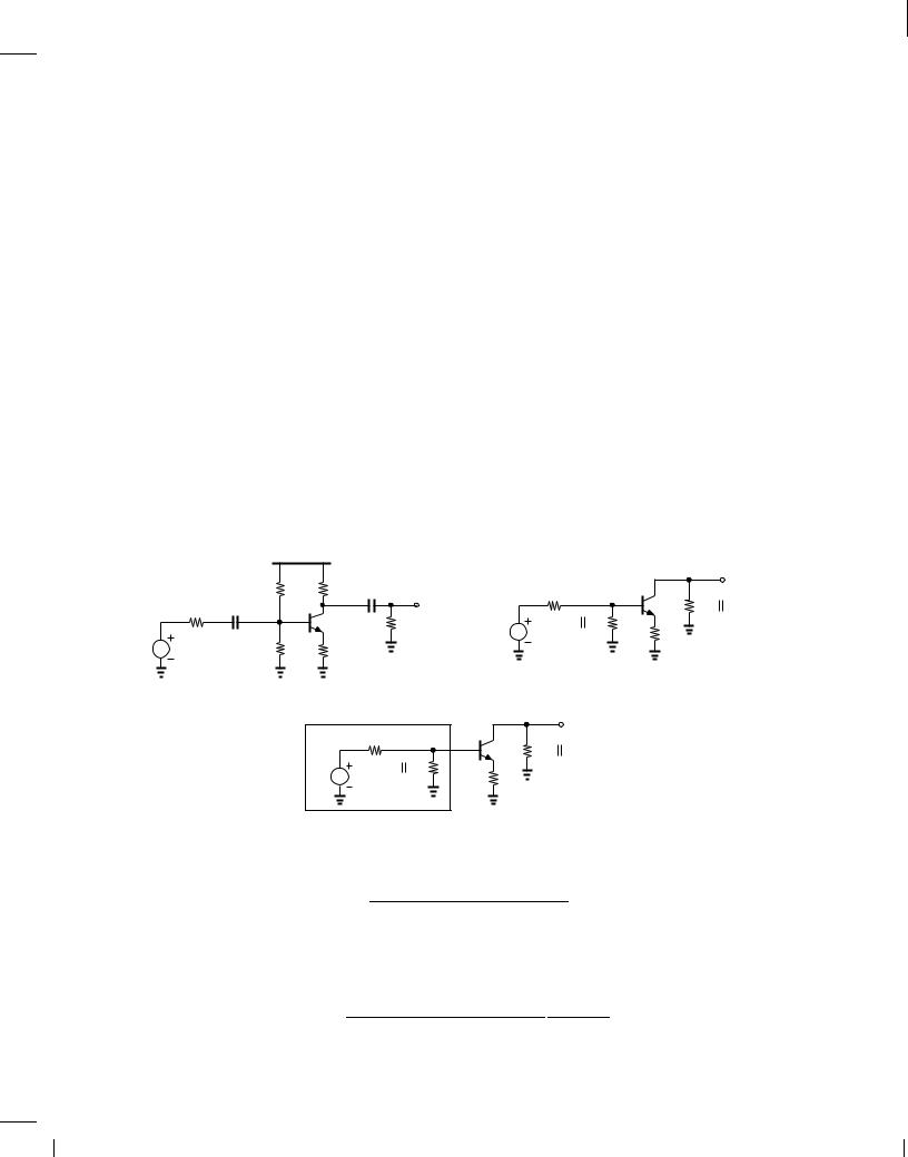
How should the circuit of Fig. 5.50 be fixed? Since only the signal generated by the microphone is of interest, a series capacitor can be inserted as depicted in Fig. 5.51 so as to isolate the dc biasing of the amplifier from the microphone. That is, the bias point of Q1 remains independent of the resistance of the microphone because C1 carries no bias current. The value of C1 is chosen so that it provides a relatively low impedance (almost a short circuit) for the frequencies of interest. We say C1 is a “coupling” capacitor and the input of this stage is “ac-coupled” or “capacitively-coupled.” Many circuits employ capacitors to isolate the bias conditions from “undesirable” effects. More examples clarify this point later.
VCC = 2.5 V 100 k Ω RB R C  1 kΩ
1 kΩ
X 
 Vout
Vout


 Q 1 C1
Figure 5.51 Capacitive coupling at the input of microphone amplifier.
The foregoing observation suggests that the methodology illustrated in Fig. 5.9 must include an additional rule: replace all capacitors with an open circuit for dc analysis and a short circuit for small-signal analysis.
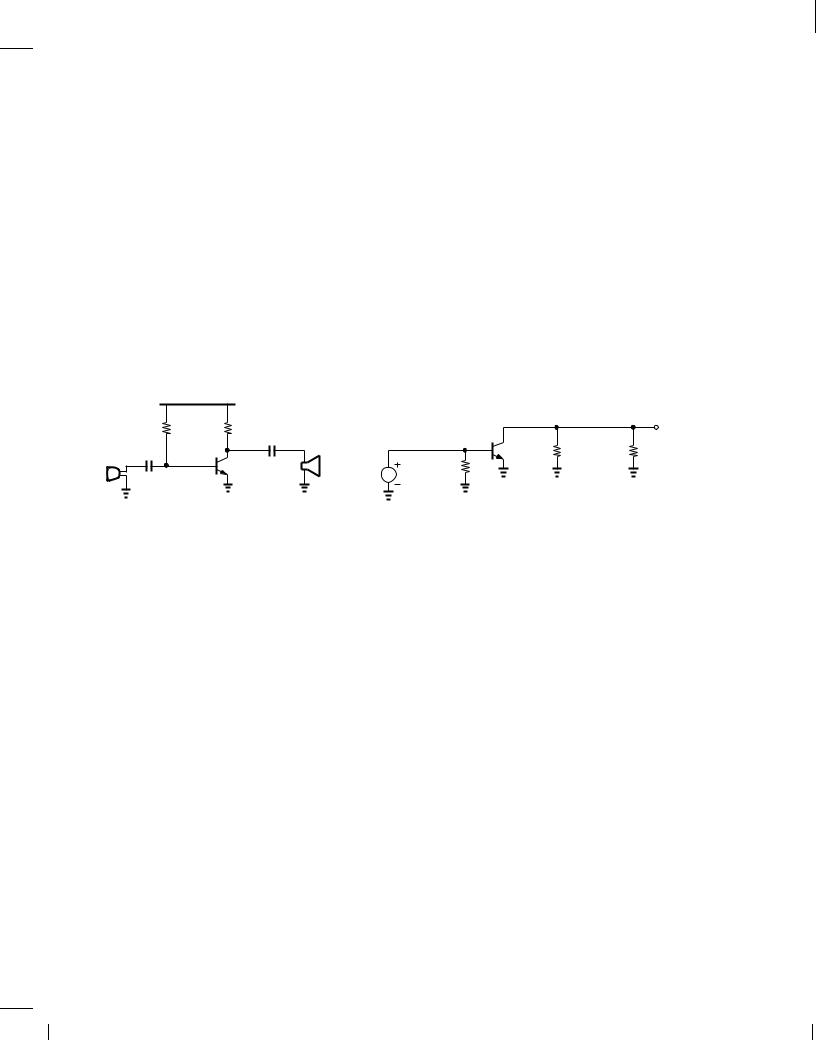
Let us begin with the stage depicted in Fig. 5.52(a). For bias calculations, the signal source is set to zero and C1 is opened, leading to Fig. 5.52(b). From Section 5.2.1, we have
|
|
VCC |
VCC |
v out |
RB |
R C |
|
RB R C |
X |
|
Q 1 RC |
|||
X |
Y |
Vout |
Y |
RB |
|
Q 1 |
X |
v in |
|
C1 |
|
Q 1 |
|
|
|
|
|
|
|
(a) |
|
|
(b) |
(c) |
|
|
|
||
|
|
Q 1 |
RC |
Q 1 RC |
|
RB |
RB |
R out |
|
R in2 |
|
R in1 |
|
|
|
|
(d) |
|
(e) |
Figure 5.52 (a) Capacitive coupling at the input of a CE stage, (b) simplified stage for bias calculation,
(c) simplified stage for small-signal calculation, (d) simplified circuit for input impedance calculation, (e) simplified circuit for output impedance calculation.
I = VCC , VBE ; |
(5.213) |
C RB
BR |
Wiley/Razavi/Fundamentals of Microelectronics [Razavi.cls v. 2006] |
June 30, 2007 at 13:42 |
222 (1) |
|
|
|
|
222 Chap. 5 Bipolar Amplifiers
V |
Y |
= V |
, R |
VCC |
, VBE |
: |
(5.214) |
|
CC |
C |
|
|
|
||
|
|
|
|
RB |
|
|
|
To avoid saturation, VY VBE.
With the bias current known, the small-signal parameters gm, r , and rO can be calculated. We now turn our attention to small-signal analysis, considering the simplified circuit of Fig. 5.52(c). Here, C1 is replaced with a short and VCC with ac ground, but Q1 is maintained as a symbol. We attempt to solve the circuit by inspection: if unsuccessful, we will resort to using a small-signal model for Q1 and writing KVLs and KCLs.
The circuit of Fig. 5.52(c) resembles the CE core illustrated in Fig. 5.29, except for RB. Interestingly, RB has no effect on the voltage at node X so long as vin remains an ideal voltage source; i.e., vX = vin regardless of the value of RB. Since the voltage gain from the base to the
collector is given by vout=vX = ,gmRC, we have |
|
|
|
vout = ,g |
m |
R : |
(5.215) |
vin |
C |
|
|
|
|
|
|
If VA < 1, then |
|
|
|
vout = ,gm(RCjjrO): |
(5.216) |
||
vin |
|
|
|
However, the input impedance is affected by RB [Fig. 5.52(d)]. Recall from Fig. 5.7 that the impedance seen looking into the base, Rin1, is equal to r if the emitter is grounded. Here, RB simply appears in parallel with Rin1, yielding
Rin2 = r jjRB: |
(5.217) |
Thus, the bias resistor lowers the input impedance. Nevertheless, as shown in Problem 51, this effect is usually negligible.
To determine the output impedance, we set the input source to zero [Fig. 5.52(e)]. Comparing this circuit with that in Fig. 5.32(b), we recognize that Rout remains unchanged:
Rout = RCjjrO: |
(5.218) |
because both terminals of RB are shorted to ground.
In summary, the bias resistor, RB, negligibly impacts the performance of the stage shown in Fig. 5.52(a).
Example 5.32
Having learned about ac coupling, the student in Example 5.31 modifies the design to that shown in Fig. 5.53 and attempts to drive a speaker. Unfortunately, the circuit still fails. Explain why.
VCC = 2.5 V 100 k Ω RB R C  1 kΩ
1 kΩ
X
 Q 1
Q 1
C1
Figure 5.53 Amplifier with direct connection of speaker.
BR |
Wiley/Razavi/Fundamentals of Microelectronics [Razavi.cls v. 2006] |
June 30, 2007 at 13:42 |
223 (1) |
|
|
|
|
Sec. 5.3 |
Bipolar Amplifier Topologies |
223 |
Solution
Typical speakers incorporate a solenoid (inductor) to actuate a membrane. The solenoid exhibits a very low dc resistance, e.g., less than 1 . Thus, the speaker in Fig. 5.53 shorts the collector to ground, driving Q1 into deep saturation.
Exercise
Does the circuit operate better if the speaker is tied between the output node and VCC?
Example 5.33
The student applies ac coupling to the output as well [Fig. 5.54(a)] and measures the quiescent points to ensure proper biasing. The collector bias voltage is 1.5 V, indicating that Q1 operates in the active region. However, the student still observes no gain in the circuit. (a) If IS = 5 10,17
VCC = 2.5 V |
|
||
100 k Ω RB R C 1 kΩ |
v out |
||
X |
C2 |
Q 1 R C 1 kΩ R sp 8 Ω |
|
100 k Ω RB |
|||
Q 1 |
|||
C1 |
|
v in |
|
|
|
||
(a) |
|
(b) |
|
Figure 5.54 (a) Amplifier with capacitive coupling at the input and output, (b) simplified small-signal model.
A and VA = 1, compute the of the transistor. (b) Explain why the circuit provides no gain.
Solution
(a) A collector voltage of 1.5 V translates to a voltage drop of 1 V across RC and hence a collector current of 1 mA. Thus,
V |
= V |
T |
ln IC |
(5.219) |
BE |
|
IS |
|
|
|
|
|
|
|
|
= 796 mV: |
(5.220) |
||
It follows that |
|
|
|
|
IB = |
VCC |
, VBE |
(5.221) |
|
|
|
RB |
|
|
= 17 A; |
(5.222) |
|||
and = IC =IB = 58:8.
(b) Speakers typically exhibit a low impedance in the audio frequency range, e.g., 8 . Drawing the ac equivalent as in Fig. 5.54(b), we note that the total resistance seen at the collector node is equal to 1 k jj8 , yielding a gain of
jAvj = gm(RCjjRS) = 0:31 |
(5.223) |
BR |
Wiley/Razavi/Fundamentals of Microelectronics [Razavi.cls v. 2006] |
June 30, 2007 at 13:42 |
224 (1) |
|
|
|
|
224 |
Chap. 5 |
Bipolar Amplifiers |
Exercise
Repeat the above example for RC = 500 .
The design in Fig. 5.54(a) exemplifies an improper interface between an amplifier and a load: the output impedance is so much higher than the load impedance that the connection of the load to the amplifier drops the gain drastically.
How can we remedy the problem of loading here? Since the voltage gain is proportional to gm, we can bias Q1 at a much higher current to raise the gain. This is studied in Problem 53. Alternatively, we can interpose a “buffer” stage between the CE amplifier and the speaker (Section 5.3.3).
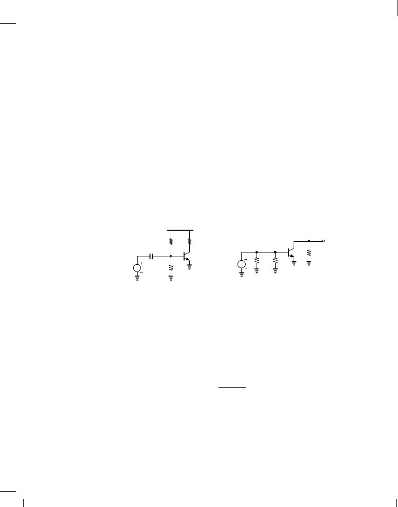
Let us now consider the biasing scheme shown in Fig. 5.15 and repeated in Fig. 5.55(a). To determine the bias conditions, we set the signal source to zero and open the capacitor(s). Equations (5.38)-(5.41) can then be used. For small-signal analysis, the simplified circuit in Fig. 5.55(b) reveals a resemblance to that in Fig. 5.52(b), except that both R1 and R2 appear in parallel with the input. Thus, the voltage gain is still equal to ,gm(RCjjrO) and the input impedance is given by
|
|
|
VCC |
|
|
|
|
|
R |
1 |
R |
C |
|
|
v out |
|
|
|
|
|
|
||
|
|
|
Q 1 |
|
|
|
Q 1 RC |
|
C1 R 2 |
|
R |
1 |
R2 |
||
v in |
|
|
v in |
|
|
||
|
|
(a) |
|
|
|
|
(b) |
Figure 5.55 (a) Biased stage with capacitive coupling, (b) simplified circuit.
Rin = r jjR1jjR2: |
(5.224) |
The output resistance is equal to RCjjrO.
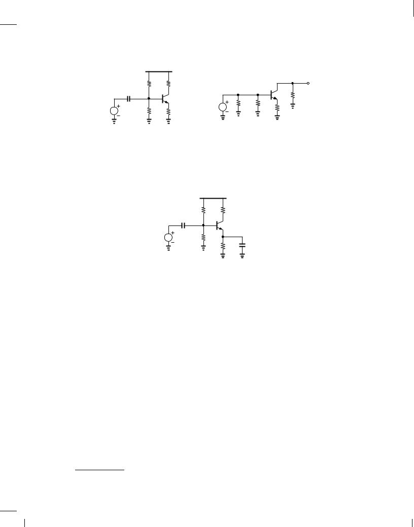
We next study the more robust biasing scheme of Fig. 5.19, repeated in Fig. 5.56(a) along with an input coupling capacitor. The bias point is determined by opening C1 and following Eqs. (5.52) and (5.53). With the collector current known, the small-signal parameters of Q1 can be computed. We also construct the simplified ac circuit shown in Fig. 5.56(b), noting that the voltage gain is not affected by R1 and R2 and remains equal to
Av = |
,RC |
; |
(5.225) |
|
1 |
+ RE |
|
|
|
|
gm |
|
|
|
where Early effect is neglected. On the other hand, the input impedance is lowered to:
Rin = [r + ( + 1)RE]jjR1jjR2; |
(5.226) |
whereas the output impedance remains equal to RC if VA = 1.
As explained in Section 5.2.3, the use of emitter degeneration can effectively stabilize the bias point despite variations in and IS. However, as evident from (5.225), degeneration also lowers
BR |
Wiley/Razavi/Fundamentals of Microelectronics [Razavi.cls v. 2006] |
June 30, 2007 at 13:42 |
225 (1) |
|
|
|
|
Sec. 5.3 |
Bipolar Amplifier Topologies |
|
|
|
225 |
||||
|
|
|
|
VCC |
|
|
|
|
|
|
|
R |
1 |
R |
C |
|
|
|
v out |
|
|
|
|
|
|
|
|
||
|
|
|
|
Q 1 |
|
R |
|
R2 |
Q 1 RC |
|
C1 |
|
|
|
1 |
RE |
|||
|
|
|
|
|
|||||
v in |
R 2 |
RE |
v in |
|
|
||||
|
|
|
|
|
|||||
|
|
|
|
(a) |
|
|
|
(b) |
|
Figure 5.56 (a) Degenerated stage with capacitive coupling, (b) simplified circuit.
the gain. Is it possible to apply degeneration to biasing but not to the signal? Illustrated in Fig. 5.57 is such a topology, where C2 is large enough to act as a short circuit for signal frequencies of interest. We can therefore write
|
|
|
VCC |
|
R |
1 |
RC |
|
C1 R |
|
Q 1 |
v in |
2 |
RE C2 |
|
|
|
|
Figure 5.57 Use of capacitor to eliminate degeneration.
Av = ,gmRC |
(5.227) |
and
Rin = r jjR1jjR2 |
(5.228) |
Rout = RC: |
(5.229) |
Example 5.34
Design the stage of Fig. 5.57 to satisfy the following conditions: IC = 1 mA, voltage drop across RE = 400 mV, voltage gain = 20 in the audio frequency range (20 Hz to 20 kHz), input impedance > 2 k . Assume = 100, IS = 5 10,16, and VCC = 2:5 V.
Solution
With IC = 1 mA IE, the value of RE is equal to 400 . For the voltage gain to remain unaffected by degeneration, the maximum impedance of C1 must be much smaller than 1=gm = 26 .8 Occurring at 20 Hz, the maximum impedance must remain below roughly 0:1 (1=gm) = 2:6 :
1 |
|
1 |
|
|
1 |
for ! = 2 20 Hz: |
(5.230) |
|
|
|
|
||||
C2! |
|
10 |
|
gm |
|
||
8A common mistake here is to make the impedance of C1 much less than RE.

BR |
Wiley/Razavi/Fundamentals of Microelectronics [Razavi.cls v. 2006] |
June 30, 2007 at 13:42 |
226 (1) |
|
|
|
|
226 |
Chap. 5 |
Bipolar Amplifiers |
Thus, |
|
|
C2 6120 F: |
|
(5.231) |
(This value is unrealistically large, requiring modification of the design.) We also have |
||
jAvj = gmRC = 20; |
|
(5.232) |
obtaining |
|
|
RC = 512 : |
|
(5.233) |
Since the voltage across RE is equal to 400 mV and VBE = VT ln(IC=IS) = 736 mV, we have VX = 1:14 V. Also, with a base current of 10 A, the current flowing through R1 and R2 must exceed 100 A to lower sensitivity to :
|
|
VCC |
> 10IB |
(5.234) |
|
|
|
R1 + R2 |
|||
|
|
|
|
||
and hence |
|
|
|
|
|
|
R1 + R2 < 25 k : |
(5.235) |
|||
Under this condition, |
|
|
|
|
|
|
|
R2 |
|
(5.236) |
|
VX |
|
|
VCC = 1:14 V; |
||
|
R1 + R2 |
||||
yielding |
|
|
|
|
|
|
|
R2 = 11:4 k |
(5.237) |
||
|
|
R1 = 13:6 k : |
(5.238) |
||
We must now check to verify that this choice of R1 and R2 satisfies the condition |
Rin > 2 k . |
That is, |
|
Rin = r jjR1jjR2 |
(5.239) |
= 1:85 k : |
(5.240) |
Unfortunately, R1 and R2 lower the input impedance excessively. To remedy the problem, we can allow a smaller current through R1 and R2 than 10IB, at the cost of creating more sensitivity to . For example, if this current is set to 5IB = 50 A and we still neglect IB in the calculation of VX ,
|
VCC |
> 5IB |
(5.241) |
|
R1 + R2 |
||
|
|
|
|
and |
|
|
|
R1 + R2 < 50 k : |
(5.242) |
||
BR |
Wiley/Razavi/Fundamentals of Microelectronics [Razavi.cls v. 2006] |
June 30, 2007 at 13:42 |
227 (1) |
|
|
|
|
Sec. 5.3 |
Bipolar Amplifier Topologies |
|
227 |
Consequently, |
|
|
|
|
R2 |
= 22:4 k |
(5.243) |
|
R1 |
= 27:2 k ; |
(5.244) |
giving |
|
|
|
|
Rin = 2:14 k : |
(5.245) |
|
Exercise
Redesign the above stage for a gain of 10 and compare the results.
We conclude our study of the CE stage with a brief look at the more general case depicted in Fig. 5.58(a), where the input signal source exhibits a finite resistance and the output is tied to a load RL. The biasing remains identical to that of Fig. 5.56(a), but RS and RL lower the voltage gain vout=vin. The simplified ac circuit of Fig. 5.58(b) reveals Vin is attenuated by the voltage division between RS and the impedance seen at node X, R1jjR2jj[r + ( + 1)RE], i.e.,
R 1
RS C1
v in |
R 2 |
VCC |
|
|
|
|
|
|
v out |
RC |
C2 |
|
RS |
|
X |
|
|
v out |
|
|
|
||||
Q 1 |
RL |
R1 |
R2 |
Q 1 |
RC |
RL |
|
v in |
RE |
|
|
||||
RE |
|
|
|
|
|
||
|
|
|
|
|
|
|
(b)
(a)
RS |
|
|
v out |
|
|
X |
|
R |
|
R2 |
Q 1 RC RL |
1 |
RE |
||
v in |
|
|
(b)
Figure 5.58 (a) General CE stage, (b) simplified circuit, (c) Thevenin model of input network.
vX = |
R1jjR2jj |
[r + ( + 1)RE] |
: |
|
|||
vin |
R1jjR2jj[r |
+ ( + 1)RE] + RS |
|
The voltage gain from vin to the output is given by
vout = vX |
vout |
|
|
|
|
||
vin |
vin |
vX |
|
|
|
|
|
= , |
|
R1jjR2jj[r + ( + 1)RE] |
RCjjRL |
: |
|||
|
|
R1jjR2jj[r |
+ ( + 1)RE] + RS |
1 |
+ RE |
||
|
|
|
|||||
|
|
|
|
|
gm |
||
(5.246)
(5.247)
(5.248)
BR |
Wiley/Razavi/Fundamentals of Microelectronics [Razavi.cls v. 2006] |
June 30, 2007 at 13:42 |
228 (1) |
|
|
|
|
228 Chap. 5 Bipolar Amplifiers
As expected, lower values of R1 and R2 reduce the gain.
The above computation views the input network as a voltage divider. Alternatively, we can utilize a Thevenin equivalent to include the effect of RS, R1, and R2 on the voltage gain. Illustrated
in Fig. 5.58(c), the idea is to replace vin, RS and R1jjR2 with vT hev and RT hev: |
|
||
vT hev = |
R1jjR2 |
vin |
(5.249) |
|
R1jjR2 + RS |
(5.250) |
|
RT hev = RSjjR1jjR2: |
|||
The resulting circuit resembles that in Fig. 5.43(a) and follows Eq. (5.185):
Av = , |
|
RCjjRL |
|
R1jjR2 |
; |
(5.251) |
|
1 |
+ RE + RT hev |
|
R1jjR2 + RS |
|
|
|
gm |
|
|
|||
|
+ 1 |
|
|
|
|
|
where the second fraction on the right accounts for the voltage attenuation given by Eq. (5.249). The reader is encouraged to prove that (5.248) and (5.251) are identical.
The two approaches described above exemplify analysis techniques used to solve circuits and gain insight. Neither requires drawing the small-signal model of the transistor because the reduced circuits can be “mapped” into known topologies.
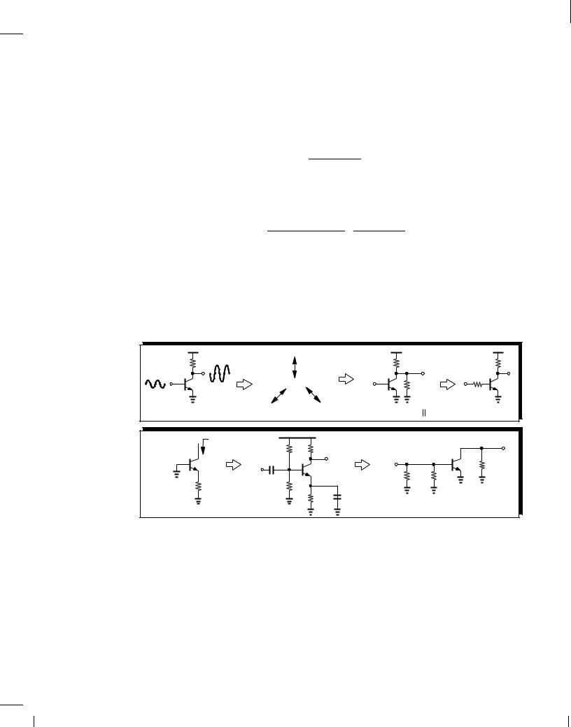
Figure 5.59 summarizes the concepts studied in this section.
Headroom |
|
R C |
R C |
Gain |
r O |
A v = − g mR C |
Rin |
Rout |
A v = − g m |
(RC |
r O ) |
A v , R in |
|
|
|||||
R out |
R 1 |
RC |
|
|
|
|
|
|
|
|
|
||
|
C1 |
|
|
|
|
Q 1 RC |
|
|
|
|
R1 |
R2 |
|
R E |
R 2 |
|
|
|
||
RE C2 |
|
|
|
|
||
|
|
|
|
|
|
Figure 5.59 Summary of concepts studied thus far.
5.3.2 Common-Base Topology
Following our extensive study of the CE stage, we now turn our attention to the “common-base“ (CB) topology. Nearly all of the concepts described for the CE configuration apply here as well. We therefore follow the same train of thought, but at a slightly faster pace.
Given the amplification capabilities of the CE stage, the reader may wonder why we study other amplifier topologies. As we will see, other configurations provide different circuit properties that are preferable to those of the CE stage in some applications. The reader is encouraged to review Examples 5.2-5.4, their resulting rules illustrated in Fig. 5.7, and the possible topologies in Fig. 5.28 before proceeding further.
BR |
Wiley/Razavi/Fundamentals of Microelectronics [Razavi.cls v. 2006] |
June 30, 2007 at 13:42 |
229 (1) |
|
|
|
|
Sec. 5.3 |
Bipolar Amplifier Topologies |
229 |
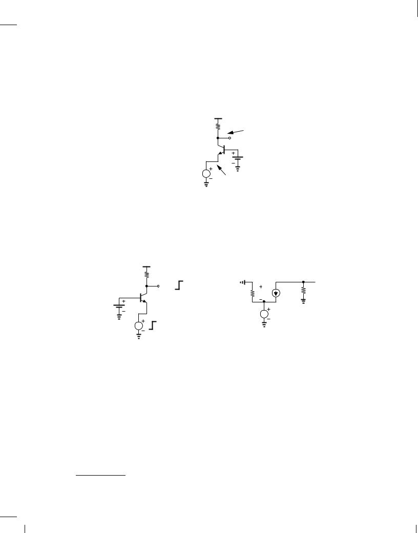
Figure 5.60 shows the CB stage. The input is applied to the emitter and the output is sensed at the collector. Biased at a proper voltage, the base acts as ac ground and hence as a node “common” to the input and output ports. As with the CE stage, we first study the core and subsequently add the biasing elements.
|
VCC |
R C |
Output Sensed |
|
at Collector |
|
Vout |
Q 1 |
Vb |
|
|
v in |
|
|
Input Applied |
|
to Emitter |
Figure 5.60 Common-base stage.
Analysis of CB Core How does the CB stage of Fig. 5.61(a) respond to an input signal?9 If Vin goes up by a small amount V , the base-emitter voltage of Q1 decreases by the same amount because the base voltage is fixed. Consequently, the collector current falls by gm V , allowing Vout to rise by gm V RC. We therefore surmise that the small-signal voltage gain is equal to
|
VCC |
|
|
|
|
R C |
|
|
|
|
Vout |
g |
V R C |
|
|
|
m |
r π vπ |
gm vπ |
|
Q 1 |
|
||
Vb |
|
|
|
|
|
|
v in |
|
|
|
|
|
|
|
Vin |
V |
|
|
|
|
(a) |
|
|
(b) |
Figure 5.61 (a) Response of CB stage to small input change, (b) small-signal model.
Av = gmRC:
 v out
v out
RC
(5.252)
Interestingly, this expression is identical to the gain of the CE topology. Unlike the CE stage, however, this circuit exhibits a positive gain because an increase in Vin leads to an increase in
Vout.
Let us confirm the above results with the aid of the small-signal equivalent depicted in Fig. 5.61(b), where the Early effect is neglected. Beginning with the output node, we equate the current flowing through RC to gmv :
,vout = gmv ; |
(5.253) |
RC |
|
9Note that the topologies of Figs. 5.60-5.61(a) are identical even though Q1 is drawn differently.

BR |
Wiley/Razavi/Fundamentals of Microelectronics [Razavi.cls v. 2006] |
June 30, 2007 at 13:42 |
230 (1) |
|
|
|
|
230 |
Chap. 5 |
Bipolar Amplifiers |
obtaining v = ,vout=(gmRC). Considering the input node next, we recognize that v = ,vin. It follows that
vout = g |
m |
R : |
(5.254) |
vin |
C |
|
|
|
|
|
As with the CE stage, the CB topology suffers from trade-offs between the gain, the voltage headroom, and the I/O impedances. We first examine the circuit's headroom limitations. How should the base voltage, Vb, in Fig. 5.61(a) be chosen? Recall that the operation in the active region requires VBE > 0 and VBC 0 (for npn devices). Thus, Vb must remain higher than the input by about 800 mV, and the output must remain higher than or equal to Vb. For example, if the dc level of the input is zero (Fig. 5.62), then the output must not fall below approximately 800 mV, i.e., the voltage drop across RC cannot exceed VCC , VBE. Similar to the CE stage limitation, this condition translates to
|
|
|
|
|
|
|
|
|
|
|
VCC |
|
||||||||||||
|
|
|
|
|
|
|
|
|
|
|
|
|||||||||||||
R C |
|
|
|
|
|
|
|
VCC − VBE |
|
|||||||||||||||
|
|
|
|
|
|
|
|
|||||||||||||||||
|
|
|
|
|
|
|
|
|
|
|
~ 0 V |
|
||||||||||||
|
|
|
|
|
|
|
|
|
|
|
|
|||||||||||||
~800 mV |
|
|
|
|
|
|
|
|
|
|
|
|
|
|
|
|
|
Vb |
||||||
|
|
|
|
|
|
|
|
|
|
|
|
|
|
|
|
|
||||||||
|
|
|
|
|
|
|
|
800 mV |
|
|
|
|
|
|
|
|||||||||
|
|
|
|
|
|
|
|
|
|
|
|
|
|
|||||||||||
|
|
|
|
|
|
|
|
|
|
|
|
|
|
|
|
|
|
|
|
|
|
|
|
|
0  Vin
Vin
t
Figure 5.62 Voltage headroom in CB stage.
Av = IC RC VT
= VCC V,T VBE :
(5.255)
(5.256)
Example 5.35
The voltage produced by an electronic thermometer is equal to 600 mV at room temperature. Design a CB stage to sense the thermometer voltage and amplify the change with maximum gain. Assume VCC = 1:8 V, IC = 0:2 mA, IS = 5 10,17 A, and = 100.
Solution
Illustrated in Fig. 5.63(a), the circuit must operate properly with an input level of 600 mV. Thus, Vb = VBE + 600 mV = VT ln(IC =IS) + 600 mV = 1:354 V. To avoid saturation, the collector voltage must not fall below the base voltage, thereby allowing a maximum voltage drop across RC equal to 1:8 V , 1:354 V = 0:446 V. We can then write
Av = gmRC |
(5.257) |
= ICRC |
(5.258) |
VT |
|
= 17:2: |
(5.259) |