

Fundamentals of Microelectronics
.pdfBR |
Wiley/Razavi/Fundamentals of Microelectronics [Razavi.cls v. 2006] |
June 30, 2007 at 13:42 |
131 (1) |
|
|
|
|
Sec. 4.3 Operation of Bipolar Transistor in Active Mode 131
Solution
Since IX = IC1 + IC2, we have |
|
|
|
|
|
I 2AEqDnni2 |
exp |
V1 |
: |
(4.11) |
|
|
|||||
X |
NBWB |
|
VT |
|
|
|
|
|
|
||
This result can also be viewed as the collector current of a single transistor having an emitter area of 2AE. In fact, redrawing the circuit as shown in Fig. 4.9(b) and noting that Q1 and Q2 experience identical voltages at their respective terminals, we say the two transistors are “in parallel,” operating as a single transistor with twice the emitter area of each.
Exercise
Repeat the above example if Q1 has an emitter area of AE and Q2 an emitter area of
8AE.
Example 4.3
In the circuit of Fig. 4.9(a), Q1 and Q2 are identical and operate in the active mode. Determine V1 , V2 such that IC1 = 10IC2.
Solution
From Eq. (4.9), we have
|
|
|
|
IS exp |
V1 |
|
|
||
|
IC1 |
|
|
V |
(4.12) |
||||
|
|
= |
|
|
T |
; |
|||
|
|
|
|
||||||
|
IC2 |
|
|
IS exp |
V2 |
|
|
||
|
|
|
|
VT |
|
||||
and hence |
|
|
|
|
|
|
|
|
|
exp |
V1 , V2 |
= 10: |
(4.13) |
||||||
|
|
|
VT |
|
|
|
|
||
That is, |
|
|
|
|
|
|
|
|
|
V1 , V2 = VT ln 10 |
|
|
|
(4.14) |
|||||
|
60 mV at T = 300 K: |
(4.15) |
|||||||
Identical to Eq. (2.109), this result is, of course, expected because the exponential dependence of IC upon VBE indicates a behavior similar to that of diodes. We therefore consider the baseemitter voltage of the transistor relatively constant and approximately equal to 0.8 V for typical collector current levels.
Exercise
Repeat the above example if Q1 and Q2 have different emitter areas, i.e., AE1 = nAE2.
BR |
Wiley/Razavi/Fundamentals of Microelectronics [Razavi.cls v. 2006] |
June 30, 2007 at 13:42 |
132 (1) |
|
|
|
|
132 |
Chap. 4 |
Physics of Bipolar Transistors |
Example 4.4
Typical discrete bipolar transistors have a large area, e.g., 500 m 500 m, whereas modern integrated devices may have an area as small as 0:5 m 0:2 m. Assuming other device parameters are identical, determine the difference between the base-emitter voltage of two such transistors for equal collector currents.
Solution
From Eq. (4.9), we have VBE = VT ln(IC =IS) and hence |
|
|
|
|||
V |
BEint |
, V |
= V ln IS1 |
; |
(4.16) |
|
|
BEdis |
T |
IS2 |
|
|
|
|
|
|
|
|
|
|
where VBEint = VT ln(IC2=IS2) and VBEdis = VT ln(IC1=IS1) denote the base-emitter voltages of the integrated and discrete devices, respectively. Since IS / AE,
V |
BEint |
, V |
= V ln AE2 |
: |
(4.17) |
|
|
BEdis |
T |
AE1 |
|
|
|
|
|
|
|
|
|
|
For this example, AE2=AE1 = 2:5 106, yielding |
|
|
|
|||
VBEint , VBEdis = 383 mV: |
|
(4.18) |
||||
In practice, however, VBEint ,VBEdis falls in the range of 100 to 150 mV because of differences in the base width and other parameters. The key point here is that VBE = 800 mV is a reasonable approximation for integrated transistors and should be lowered to about 700 mV for discrete devices.
Exercise
Repeat the above comparison for a very small integrated device with an emitter area of
0:15 m 0:15
Since many applications deal with voltage quantities, the collector current generated by a bipolar transistor typically flows through a resistor to produce a voltage.
Example 4.5
Determine the output voltage in Fig. 4.10 if IS = 5 10,16 A.
R L  1 kΩ
1 kΩ
I C |
3 V |
|
|
|
|
|
|
|
|
|
|
|
|
|
|
|
750 mV |
|
|
|
|
|
|
|
|
|
Vout |
||||
|
|
|
|
|
Q 1 |
|
|
|||||||
|
|
|
|
|
|
|
|
|
|
|
|
|
||
Figure 4.10 Simple stage with biasing.
Solution
Using Eq. (4.9), we write IC = 1:69 mA. This current flows through RL, generating a voltage
BR |
Wiley/Razavi/Fundamentals of Microelectronics [Razavi.cls v. 2006] |
June 30, 2007 at 13:42 |
133 (1) |
|
|
|
|
Sec. 4.3 Operation of Bipolar Transistor in Active Mode |
133 |
drop of 1 k 1:69 mA = 1:69 V. Since VCE = 3V , IC RL, we obtain |
|
Vout = 1:31 V: |
(4.19) |
Exercise
What happens if the load resistor is halved.
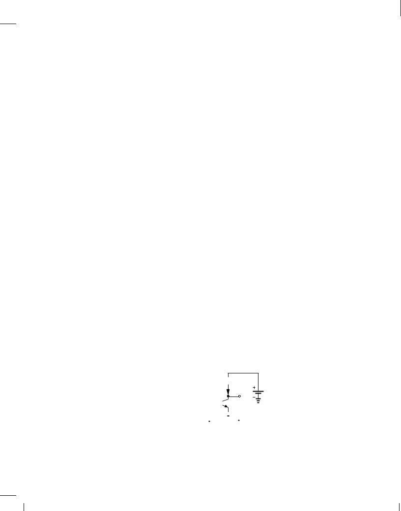
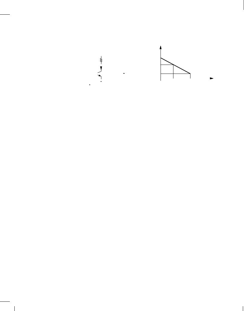
Equation (4.9) reveals an interesting property of the bipolar transistor: the collector current does not depend on the collector voltage (so long as the device remains in the active mode). Thus, for a fixed base-emitter voltage, the device draws a constant current, acting as a current source [Fig. 4.11(a)]. Plotted in Fig. 4.11(b) is the current as a function of the collector-emitter voltage, exhibiting a constant value for VCE > V1.3 Constant current sources find application in many electronic circuits and we will see numerous examples of their usage in this book. In Section 4.5, we study the behavior of the transistor for VCE < VBE.
|
|
I C |
|
|
|
|
Forward Active |
|
|
Q |
1 |
V1 |
Region |
|
V1 |
I S exp |
|
|
|
|
VT |
|
|
|
|
|
V1 |
V |
CE |
|
|
|
|
|
|
(a) |
|
(b) |
|
Figure 4.11 (a) Bipolar transistor as a current source, (b) I/V characteristic.
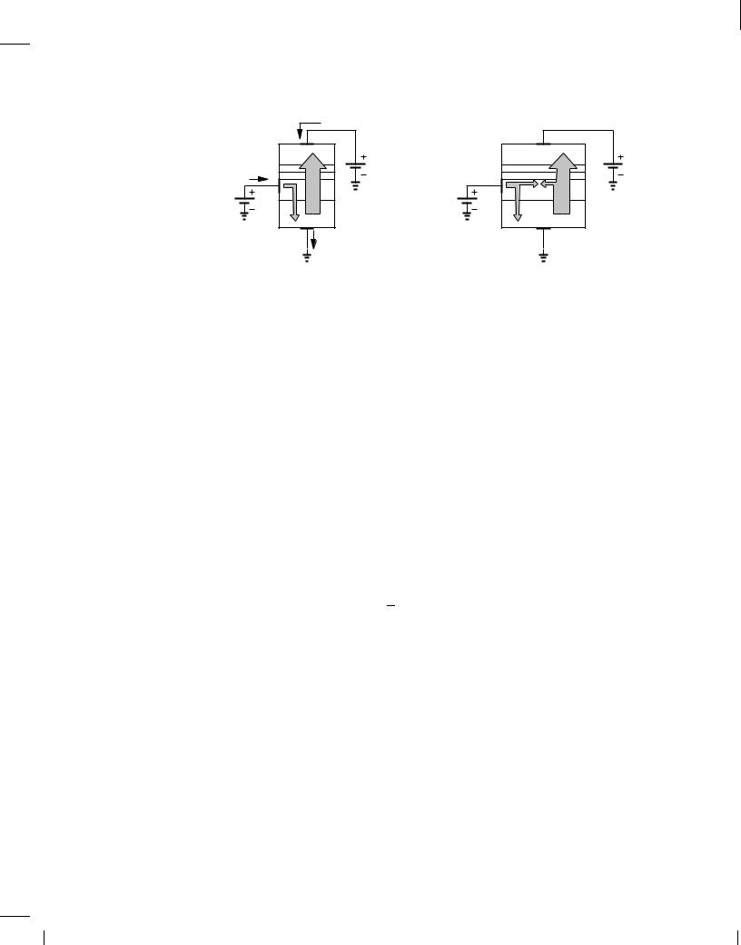
4.3.2 Base and Emitter Currents
Having determined the collector current, we now turn our attention to the base and emitter currents and their dependence on the terminal voltages. Since the bipolar transistor must satisfy Kirchoff's current law, calculation of the base current readily yields the emitter current as well.
In the npn transistor of Fig. 4.12(a), the base current, IB, results from the flow of holes. Recall from Eq. (2.99) that the hole and electron currents in a forward-biased pn junction bear a constant ratio given by the doping levels and other parameters. Thus, the number of holes entering from the base to the emitter is a constant fraction of the number of electrons traveling from the emitter to the base. As an example, for every 200 electrons injected by the emitter, one hole must be supplied by the base.
In practice, the base current contains an additional component of holes. As the electrons injected by the emitter travel through the base, some may “recombine” with the holes [Fig. 4.12(b)]; in essence, some electrons and holes are “wasted” as a result of recombination. For example, on the average, out of every 200 electrons injected by the emitter, one recombines with a hole.
In summary, the base current must supply holes for both reverse injection into the emitter and recombination with the electrons traveling toward the collector. We can therefore view IB as a
3Recall that VCE > V1 is necessary to ensure the collector-base junction remains reverse biased.
BR |
Wiley/Razavi/Fundamentals of Microelectronics [Razavi.cls v. 2006] |
June 30, 2007 at 13:42 |
134 (1) |
|
|
|
|
134 |
Chap. 4 |
Physics of Bipolar Transistors |
|
I C |
|
|
|
|
|
n |
|
n |
I B |
− |
VCE |
− |
VCE |
|
e |
p |
e |
p |
VBE |
|
|
e− |
|
h+ |
|
VBE |
|
|
|
n + |
h+ |
n + |
|
|
|
|
||
|
|
I E |
|
|
(a) |
(b) |
Figure 4.12 Base current resulting from holes (a) crossing to emitter and (b) recombining with electrons.
constant fraction of IE or a constant fraction of IC. It is common to write
IC = IB; |
(4.20) |
where is called the “current gain” of the transistor because it shows how much the base current is “amplified.” Depending on the device structure, the of npn transistors typically ranges from 50 to 200.
In order to determine the emitter current, we apply the KCL to the transistor with the current directions depicted in Fig. 4.12(a):
IE = IC + IB |
|
|
(4.21) |
= IC 1 + |
1 |
: |
(4.22) |
|
|
|
|
We can summarize our findings as follows:
IC
IB
IE
=IS exp VBE
VT
=1 IS exp VBE
VT
=+ 1IS exp VBE :
VT
(4.23)
(4.24)
(4.25)
It is sometimes useful to write IC = [ =( + 1)]IE and denote =( + 1) by . For = 100,= 0:99, suggesting that 1 and IC IE are reasonable approximations. In this book, we assume that the collector and emitter currents are approximately equal.
Example 4.6
A bipolar transistor having IS = 5 10,16 A is biased in the forward active region with VBE = 750 mV. If the current gain varies from 50 to 200 due to manufacturing variations, calculate the minimum and maximum terminal currents of the device.
Solution
For a given VBE, the collector current remains independent of : |
|
IC = IS exp VBE |
(4.26) |
VT |
|
BR |
Wiley/Razavi/Fundamentals of Microelectronics [Razavi.cls v. 2006] |
June 30, 2007 at 13:42 |
135 (1) |
|
|
|
|
Sec. 4.4 |
Bipolar Transistor Models and Characteristics |
135 |
|
= 1:685 mA: |
(4.27) |
The base current varies from IC =200 to IC=50:
8:43 A < IB < 33:7 A: |
(4.28) |
On the other hand, the emitter current experiences only a small variation because ( + 1)= is near unity for large :
1:005IC < IE < 1:02IC |
(4.29) |
1:693 mA < IE < 1:719 mA: |
(4.30) |
Exercise
Repeat the above example if the area of the transistor is doubled.
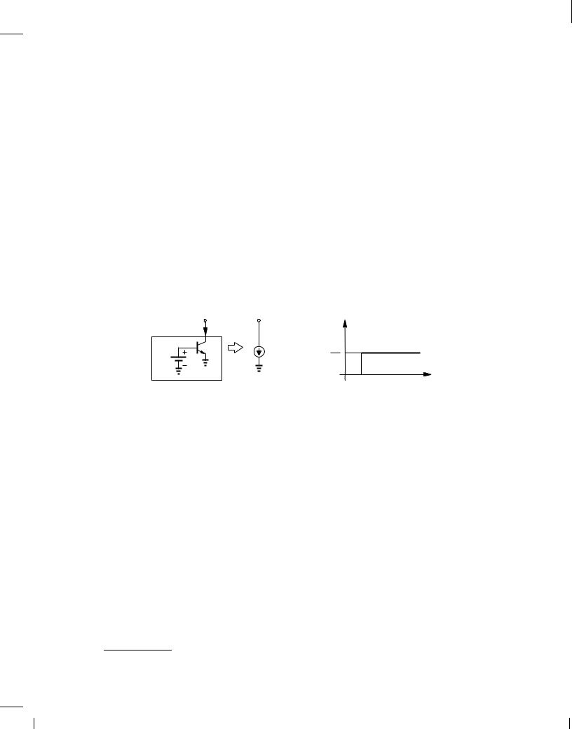
4.4 Bipolar Transistor Models and Characteristics
4.4.1 Large-Signal Model
With our understanding of the transistor operation in the forward active region and the derivation of Eqs. (4.23)-(4.25), we can now construct a model that proves useful in the analysis and design of circuits—in a manner similar to the developments in Chapter 2 for the pn junction.
Since the base-emitter junction is forward-biased in the active mode, we can place a diode between the base and emitter terminals. Moreover, since the current drawn from the collector and flowing into the emitter depends on only the base-emitter voltage, we add a voltage-controlled current source between the collector and the emitter, arriving at the model shown in Fig. 4.13. As illustrated in Fig. 4.11, this current remains independent of the collector-emitter voltage.
B |
|
C |
|
V |
VBE |
|
I S exp |
|
|
BE |
VT |
|
|
|
I S |
VBE |
|
β |
exp |
|
VT |
E |
|
|
|
Figure 4.13 Large-signal model of bipolar transistor in active region.
But how do we ensure that the current flowing through the diode is equal to 1= times the collector current? Equation (4.24) suggests that the base current is equal to that of a diode having a reverse saturation current of IS= . Thus, the base-emitter junction is modeled by a diode whose cross section area is 1= times that of the actual emitter area.
With the interdependencies of currents and voltages in a bipolar transistor, the reader may wonder about the cause and effect relationships. We view the chain of dependencies as VBE ! IC ! IB ! IE; i.e., the base-emitter voltage generates a collector current, which requires a proportional base current, and the sum of the two flows through the emitter.
Example 4.7
Consider the circuit shown in Fig. 4.14(a), where IS;Q1 = 5 10,17 A and VBE = 800 mV.
BR |
Wiley/Razavi/Fundamentals of Microelectronics [Razavi.cls v. 2006] |
June 30, 2007 at 13:42 |
136 (1) |
|
|
|
|
136 |
|
|
|
|
|
|
|
|
|
|
|
|
|
|
|
|
|
|
|
Chap. 4 |
Physics of Bipolar Transistors |
|||
|
|
|
|
|
|
|
|
|
|
|
|
|
|
|
|
|
|
|
|
VX |
|
|
|
|
|
|
|
|
|
|
|
|
|
|
|
|
|
|
|
|
|
|
|
|
(V) |
|
|
|
|
|
|
|
|
|
|
|
|
|
|
|
|
|
2.0 |
|
|
|
||||||||
|
|
|
|
R C |
|
|
|
|
500 Ω |
|
|
|
|
|
|
|
|
|
||||||
|
|
|
|
|
|
|
|
|
|
|
|
|
|
|
|
|||||||||
|
|
|
|
|
|
|
|
|
|
|
|
|
1.424 |
|
|
|
||||||||
|
|
|
|
I C |
|
|
|
|
VCC |
|
|
|
|
|
|
|
|
2 V |
|
|
|
|||
|
|
|
|
|
|
|
|
|
|
X |
|
|
|
|
|
|
|
0.800 |
|
|
|
|||
VBE |
|
|
|
|
|
|
|
Q 1 |
|
|
|
|
|
|
|
|
|
|||||||
|
|
|
|
|
|
|
|
|||||||||||||||||
|
|
|
|
|
|
|
|
|
|
|
|
|
|
|
|
|
|
|
|
|
|
|
|
|
|
|
|
|
|
|
|
|
|
|
|
|
|
|
|
|
|
|
|
|
|
|
500 |
1041 R C (Ω ) |
|
|
|
|
|
|
|
|
|
|
|
|
|
|
|
|
|
|
|
|
|
|
|
|||
|
|
|
|
|
(a) |
|
|
|
|
|
|
|
|
|
|
(b) |
||||||||
|
|
|
|
|
|
|
|
|
|
|
|
|
|
|
|
|
||||||||
Figure 4.14 (a) Simple stage with biasing, (b) variation of collector voltage as a function of collector resistance.
Assume = 100. (a) Determine the transistor terminal currents and voltages and verify that the device indeed operates in the active mode. (b) Determine the maximum value of RC that permits operation in the active mode.
Solution
(a) Using Eq. (4.23)-(4.25), we have
IC = 1:153 mA |
(4.31) |
IB = 11:53 A |
(4.32) |
IE = 1:165 mA: |
(4.33) |
The base and emitter voltages are equal to +800 mV and zero, respectively. We must now calculate the collector voltage, VX . Writing a KVL from the 2-V power supply and across RC and Q1, we obtain
VCC = RCIC + VX : |
(4.34) |
That is, |
|
VX = 1:424 V: |
(4.35) |
Since the collector voltage is more positive than the base voltage, this junction is reverse-biased and the transistor operates in the active mode.
(b)What happens to the circuit as RC increases? Since the voltage drop across the resistor, RC IC, increases while VCC is constant, the voltage at node X drops. The device approaches the “edge” of the forward active region if the base-collector voltage falls to zero, i.e., as VX ! +800 mV. Rewriting Eq. (4.34) yields:
RC = |
VCC , VX ; |
(4.36) |
|
IC |
|
which, for VX = +800 mV, reduces to |
|
|
RC = 1041 : |
(4.37) |
|
Figure 4.14(b) plots VX as a function of RC. |
|
|
BR |
Wiley/Razavi/Fundamentals of Microelectronics [Razavi.cls v. 2006] |
June 30, 2007 at 13:42 |
137 (1) |
|
|
|
|
Sec. 4.4 |
Bipolar Transistor Models and Characteristics |
137 |
This example implies that there exists a maximum allowable value of the collector resistance, RC, in the circuit of Fig. 4.14(a). As we will see in Chapter 5, this limits the voltage gain that the circuit can provide.
Exercise
In the above example, what is the minimum allowable value of VCC for transistor operation in the active mode? Assume RC = 500 .
The reader may wonder why the equivalent circuit of Fig. 4.13 is called the “large-signal model.” After all, the above example apparently contains no signals! This terminology emphasizes that the model can be used for arbitrarily large voltage and current changes in the transistor (so long as the device operates in the active mode). For example, if the base-emitter voltage varies from 800 mV to 300 mV, and hence the collector current by many orders of magnitude,4 the model still applies. This is in contrast to the small-signal model, studied in Section 4.4.4.
4.4.2 I/V Characteristics
The large-signal model naturally leads to the I/V characteristics of the transistor. With three terminal currents and voltages, we may envision plotting different currents as a function of the potential difference between every two terminals—an elaborate task. However, as explained below, only a few of such characteristics prove useful.
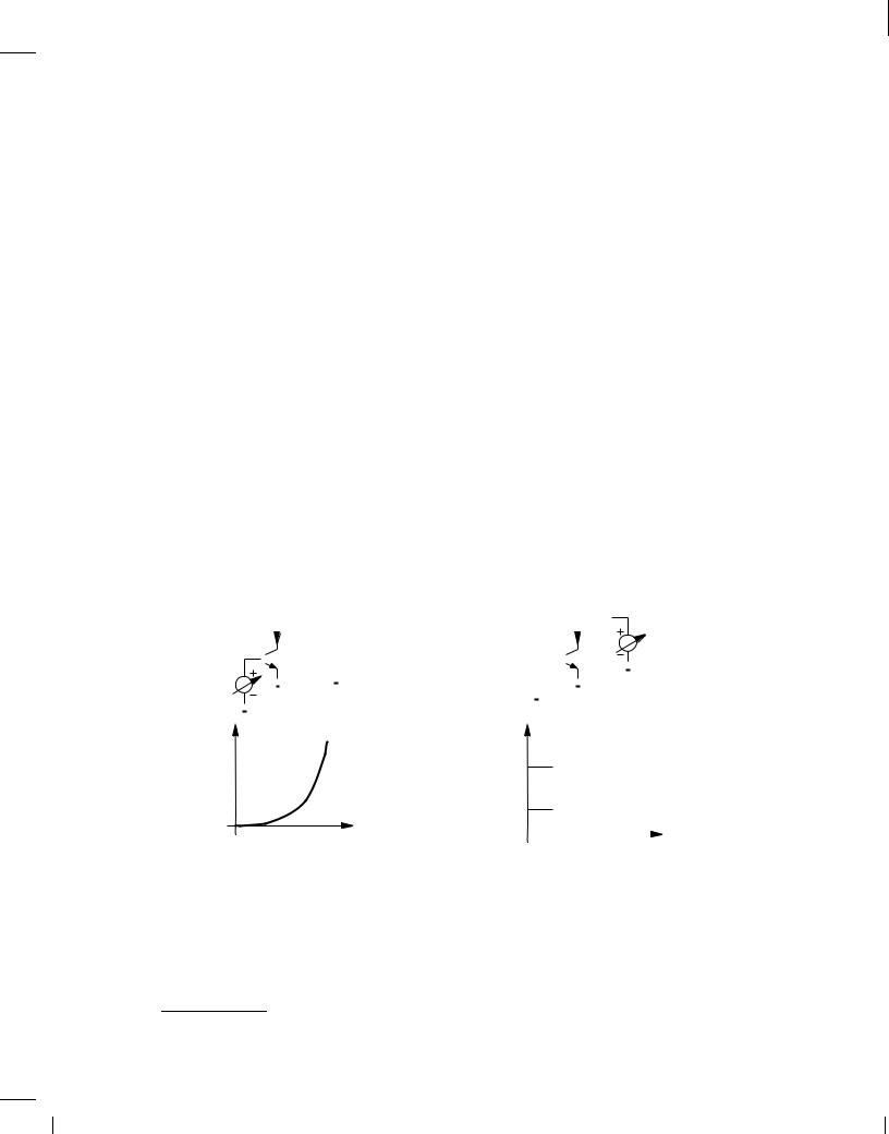
The first characteristic to study is, of course, the exponential relationship inherent in the device. Figure 4.15(a) plots IC versus VBE with the assumption that the collector voltage is constant and no lower than the base voltage. As shown in Fig. 4.11, IC is independent of VCE; thus, different values of VCE do not alter the characteristic.
|
|
|
|
|
I C |
|
|
|
|
|
VCE |
|
|
|
|
|
|
|
|
|
|
|
I C |
|
|
|
|
|
|
|
|
|
|
VCE |
|
|||||||
|
|
|
|
|
|
|
|
|
|
|
|
|
|
|
|
|
|
|
|
|
|
|
|
|
|
|
|
|
|
|
|
|||||||||||
|
|
|
|
|
|
|
|
|
|
|
|
|
|
|
|
|
|
|
|
|
|
|
|
|
|
|
|
|
|
|
|
|
|
|
|
|
|
|
|
|||
|
|
|
|
|
|
|
|
|
Q 1 |
|
|
|
VBE |
|
|
|
|
|
|
|
|
|
|
|
|
Q 1 |
|
|
|
|
|
|
|
|||||||||
|
|
|
|
|
|
|
|
|
|
|
|
|
|
|
|
|
|
|
|
|
|
|
|
|
|
|
|
|
|
|
|
|
|
|
|
|
|
|
|
|||
|
|
|
|
|
|
|
|
|
|
|
|
|
|
|
|
|
|
|
|
|
|
|
|
|
|
|
|
|
|
|
|
|
|
|
|
|
|
|
|
|||
VBE |
|
|
|
|
|
|
|
|
|
|
|
|
|
|
|
|
|
|
|
|
|
|
|
|
|
|
|
|
|
|
|
|
|
|
|
|||||||
|
|
|
|
|
|
|
|
|
|
|
|
|
|
|
|
|
|
|
|
|
|
|
|
|
|
|
|
|
|
|
|
|
|
|
|
|
|
|
|
|
|
|
|
|
|
|
|
|
|
|
|
|
|
|
|
|
|
|
|
I C |
|
|
|
|
|
|
|
|
|
|
|
|
|
|
|
|
|
|
|
|
|||||
|
|
|
|
|
|
|
|
|
|
|
|
|
|
|
|
|
|
|
|
|
|
|
|
|
|
|
|
|||||||||||||||
I C |
|
|
|
|
|
|
|
|
|
|
|
|
|
|
|
|
|
|
|
|
|
|
|
|
||||||||||||||||||
|
|
|
|
|
|
|
|
|
|
|
|
|
|
|
|
I S exp |
VBE2 |
|
|
|
|
|
|
|
|
|
|
|
|
|
|
|
|
|
|
VBE |
= VB2 |
|||||
|
|
|
|
|
|
|
|
|
|
|
|
|
|
|
|
VT |
|
|
|
|
|
|
|
|
|
|
|
|
|
|
|
|
|
|||||||||
|
|
|
|
|
|
|
|
|
|
|
|
|
|
|
|
|
|
|
|
|
|
|
|
|
|
|
|
|
|
|
|
|
|
|
|
|
||||||
|
|
|
|
|
|
|
|
|
|
|
|
|
|
|
|
I S exp |
VBE1 |
|
|
|
|
|
|
|
|
|
|
|
|
|
|
|
|
|
|
VBE |
= VB1 |
|||||
|
|
|
|
|
|
|
|
|
|
|
|
|
|
|
|
VT |
|
|
|
|
|
|
|
|
|
|
|
|
|
|
|
|
|
|||||||||
|
|
|
|
|
|
|
|
|
|
|
|
|
|
|
|
|
|
|
|
|
|
|
|
|
|
|
|
|
|
|
|
|
|
|
|
|
||||||
|
|
|
|
|
|
|
|
|
|
|
|
|
|
|
VBE |
|
|
|
|
|
|
|
|
|
|
|
|
|
|
|
|
|
|
|
|
|
|
|
|
|
|
|
|
|
|
|
|
|
|
|
|
|
|
|
|
|
|
|
|
|
|
|
|
|
|
|
|
|
|
|
|
|
|
|
|
|
|
|
|
VCE |
|
||||
|
|
|
|
|
|
|
|
|
|
|
|
|
|
|
|
|
|
|
|
|
|
|
|
|
|
|
|
|
|
|
|
|
|
|
|
|
|
|
|
|||
|
|
|
|
|
|
|
|
|
|
|
(a) |
|
|
|
|
|
|
|
|
|
|
|
|
|
|
|
|
|
|
|
|
|
(b) |
|
||||||||
Figure 4.15 Collector current as a function of (a) base-emitter voltage and (b) collector-emitter voltage.
Next, we examine IC for a given VBE but with VCE varying. Illustrated in Fig. 4.15(b), the characteristic is a horizontal line because IC is constant if the device remains in the active mode (VCE > VBE). On the other hand, if different values are chosen for VBE, the characteristic moves up or down.
4A 500-mV change in VBE leads to 500 mV=60 mV = 8:3 decades of change in IC.
BR |
Wiley/Razavi/Fundamentals of Microelectronics [Razavi.cls v. 2006] |
June 30, 2007 at 13:42 |
138 (1) |
|
|
|
|
138 |
Chap. 4 |
Physics of Bipolar Transistors |
The two plots of Fig. 4.15 constitute the principal characteristics of interest in most analysis and design tasks. Equations (4.24) and (4.25) suggest that the base and emitter currents follow the same behavior.
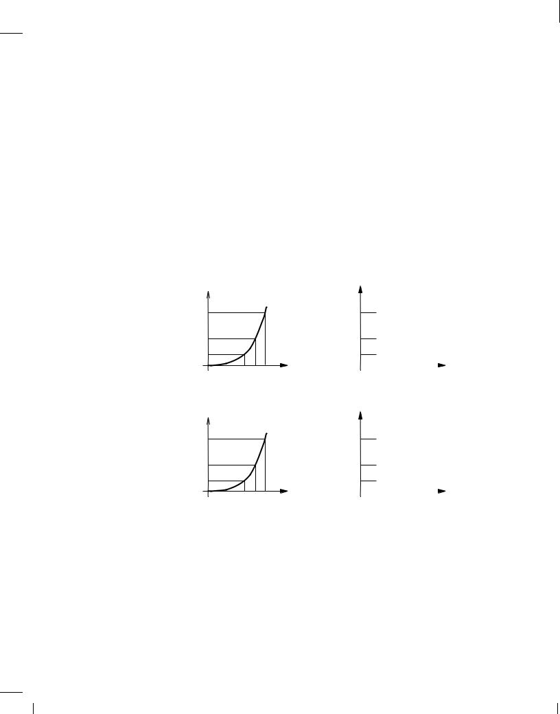
Example 4.8
For a bipolar transistor, IS = 5 10,17 A and = 100. Construct the IC -VBE, IC -VCE, IB-VBE, and IB-VCE characteristics.
Solution
We determine a few points along the IC-VBE characteristics, e.g.,
VBE1 |
= 700 mV ) IC1 |
= 24:6 A |
(4.38) |
VBE2 |
= 750 mV ) IC2 |
= 169 A |
(4.39) |
VBE3 |
= 800 mV ) IC3 |
= 1:153 mA: |
(4.40) |
The characteristic is depicted in Fig. 4.16(a).
I C 
1.153 mA
169 A
24.6 A
700 |
750 |
800 |
(a) |
|
|
IB 
11.5A
0.169 A
0.025 A
700 |
750 |
800 |
(c) |
|
|
I C |
|
|
|
|
1.153 mA |
|
VBE = 800 mV |
||
|
||||
169 A |
|
VBE = 750 mV |
||
|
||||
24.6 A |
|
VBE = 700 mV |
||
|
||||
|
|
|
|
|
VBE |
VCE |
|||
(mV) |
|
|
|
|
|
|
(b) |
||
I B |
|
|
|
|
11.5 A |
|
VBE = 800 mV |
||
|
||||
0.169 A |
|
VBE = 750 mV |
||
|
||||
0.025 A |
|
VBE = 700 mV |
||
|
||||
|
|
|
|
|
VBE |
VCE |
|||
(mV) |
|
|
|
|
|
|
(d) |
||
Figure 4.16 (a) Collector current as a function of VBE, (b) collector current as a function of VCE, (c) base current as a function of VBE, (b) base current as a function of VCE.
Using the values obtained above, we can also plot the IC-VCE characteristic as shown in Fig. 4.16(b), concluding that the transistor operates as a constant current source of, e.g., 169 A if its base-emitter voltage is held at 750 mV. We also remark that, for equal increments in VBE, IC jumps by increasingly greater steps: 24.6 A to 169 A to 1.153 mA. We return to this property in Section 4.4.3.
For IB characteristics, we simply divide the IC values by 100 [Figs. 4.16(c) and (d)].
BR |
Wiley/Razavi/Fundamentals of Microelectronics [Razavi.cls v. 2006] |
June 30, 2007 at 13:42 |
139 (1) |
|
|
|
|
Sec. 4.4 |
Bipolar Transistor Models and Characteristics |
139 |
Exercise
What change in VBE doubles the base current?
The reader may wonder what exactly we learn from the I/V characteristics. After all, compared to Eqs. (4.23)-(4.25), the plots impart no additional information. However, as we will see throughout this book, the visualization of equations by means of such plots greatly enhances our understanding of the devices and the circuits employing them.
4.4.3 Concept of Transconductance
Our study thus far shows that the bipolar transistor acts as a voltage-dependent current source (when operating in the forward active region). An important question that arises here is, how is the performance of such a device quantified? In other words, what is the measure of the “goodness” of a voltage-dependent current source?
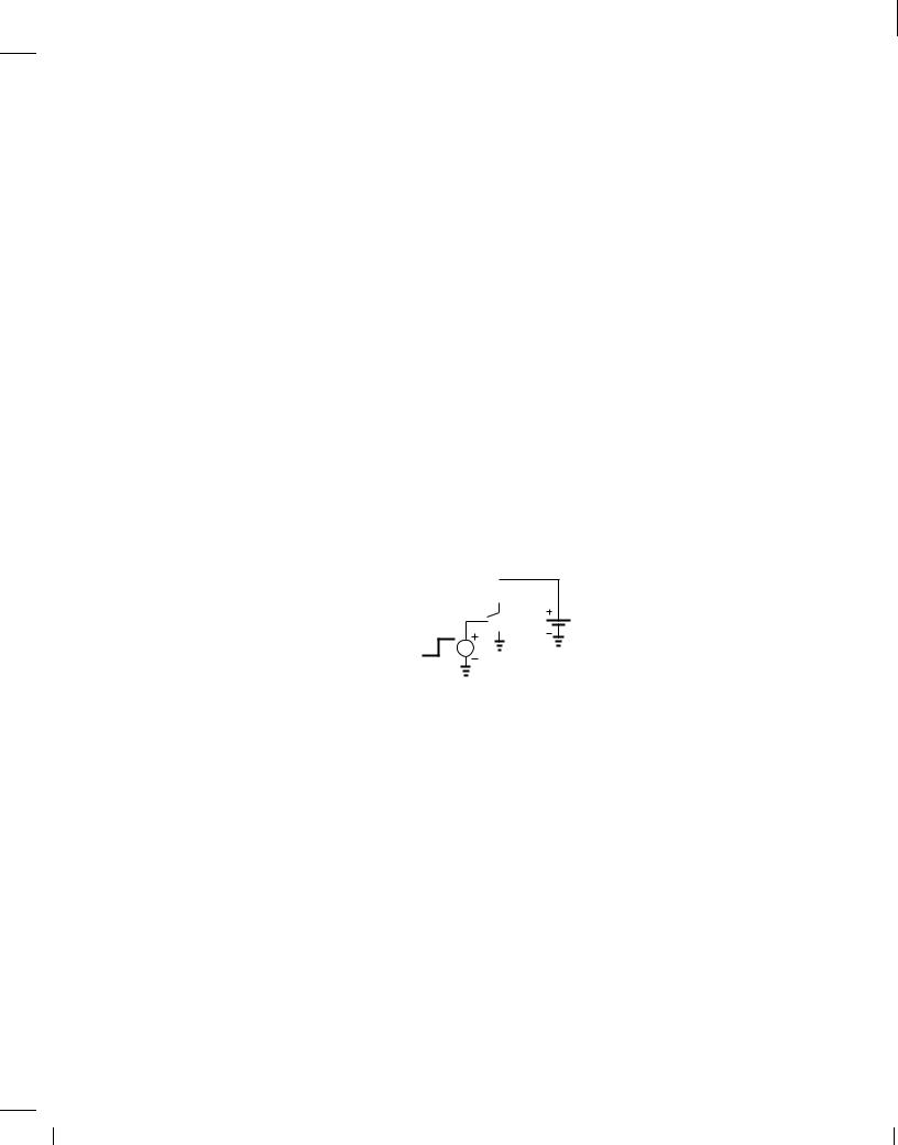
The example depicted in Fig. 4.1 suggests that the device becomes “stronger” as K increases because a given input voltage yields a larger output current. We must therefore concentrate on the voltage-to-current conversion property of the transistor, particularly as it relates to amplification of signals. More specifically, we ask, if a signal changes the base-emitter voltage of a transistor by a small amount (Fig. 4.17), how much change is produced in the collector current? Denoting the change in IC by IC, we recognize that the “strength” of the device can be represented byIC = VBE. For example, if a base-emitter voltage change of 1 mV results in a IC of 0.1 mA in one transistor and 0.5 mA in another, we can view the latter as a better voltage-dependent current source or “voltage-to-current converter.”
I C 

 Q 1 VCE
VBE
Figure 4.17 Test circuit for measurement of gm.
The ratio IC = VBE approaches dIC =dVBE for very small changes and, in the limit, is called the “transconductance,” gm:
gm = |
dIC |
: |
(4.41) |
|
|||
|
dVBE |
|
|
Note that this definition applies to any device that approximates a voltage-dependent current source (e.g., another type of transistor described in Chapter 6). For a bipolar transistor, Eq. (4.9) gives
g |
|
= |
d |
|
I exp VBE |
|
(4.42) |
||
m |
|
|
|
||||||
|
|
dVBE |
S |
VT |
|
|
|||
|
|
|
|
|
|
||||
|
|
= |
1 |
I |
|
exp VBE |
|
|
(4.43) |
|
|
|
S |
|
|
||||
|
|
|
VT |
VT |
|
|
|
||
|
|
= |
IC : |
|
|
|
|
(4.44) |
|
|
|
|
VT |
|
|
|
|
|
|
The close resemblance between this result and the small-signal resistance of diodes [Eq. (3.58)] is no coincidence and will become clearer in the next chapter.
BR |
Wiley/Razavi/Fundamentals of Microelectronics [Razavi.cls v. 2006] |
June 30, 2007 at 13:42 |
140 (1) |
|
|
|
|
140 |
Chap. 4 |
Physics of Bipolar Transistors |
Equation (4.44) reveals that, as IC increases, the transistor becomes a better amplifying device by producing larger collector current excursions in response to a given signal level applied between the base and the emitter. The transconductance may be expressed in ,1 or “siemens,” S. For example, if IC = 1 mA, then with VT = 26 mV, we have
gm = 0:0385 ,1 |
(4.45) |
= 0:0385 S |
(4.46) |
= 38:5 mS: |
(4.47) |
However, as we will see throughout this book, it is often helpful to view gm as the inverse of a resistance; e.g., for IC = 1 mA, we may write
g = |
1 |
: |
(4.48) |
m |
26 |
|
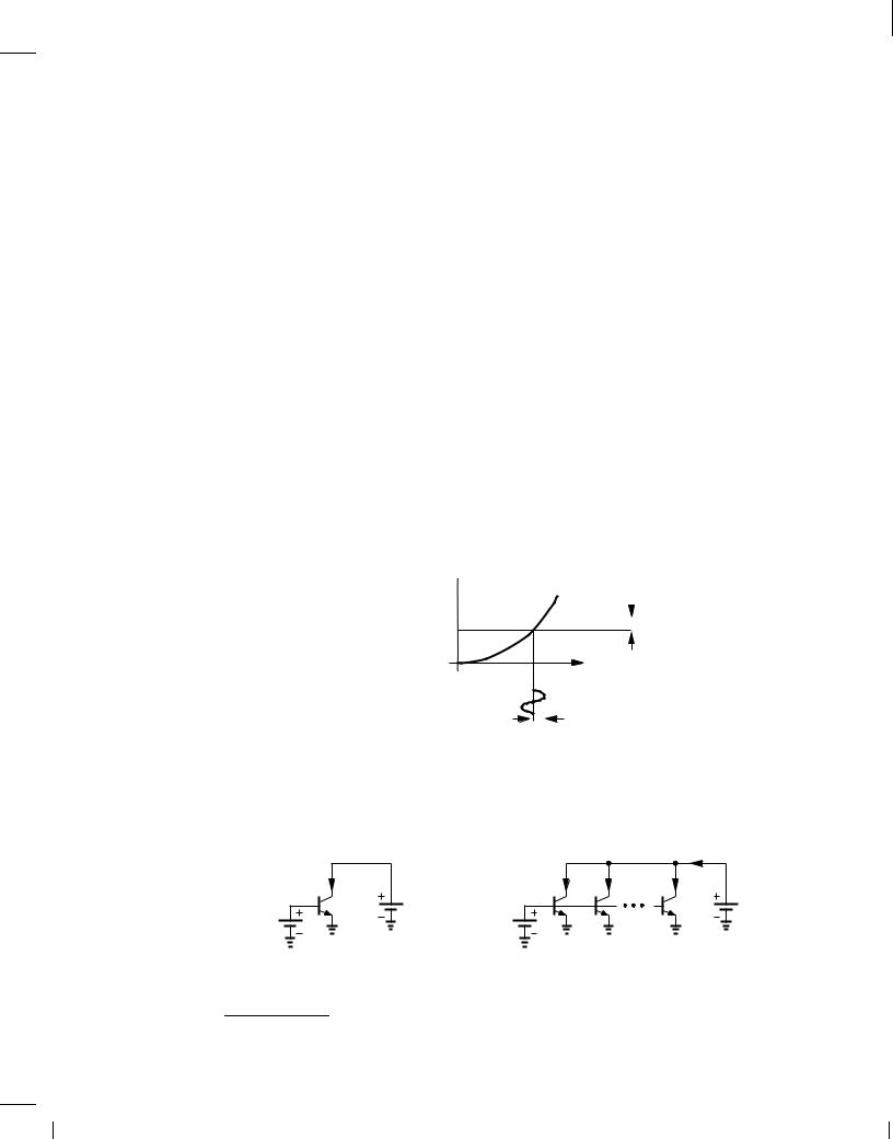
The concept of transconductance can be visualized with the aid of the transistor I/V characteristics. As shown in Fig. 4.18, gm = dIC =dVBE simply represents the slope of IC-VBE characteristic at a given collector current, IC0, and the corresponding base-emitter voltage, VBE0. In other words, if VBE experiences a small perturbation V around VBE0, then the collector current displays a change of gm V around IC0, where gm = IC0=VT . Thus, the value of IC0 must be chosen according to the required gm and, ultimately, the required gain. We say the transistor is “biased” at a collector current of IC0, meaning the device carries a bias (or “quiescent”) current of IC0 in the absence of signals.5
I C 
I C0  gm V
gm V
VBE0 VBE
V
Figure 4.18 Illustration of transconductance.
Example 4.9
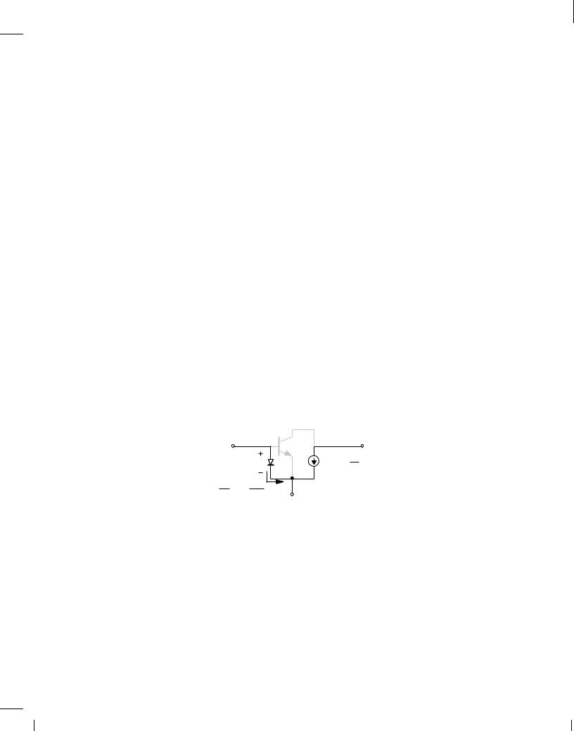
Consider the circuit shown in Fig. 4.19(a). What happens to the transconductance of Q1 if the area of the device is increased by a factor of n?
|
|
|
nI C0 |
I C0 |
|
I C0 I C0 |
I C0 |
Q 1 |
VCE |
|
VCE |
VBE0 |
|
VBE0 |
|
(a) |
|
|
(b) |
Figure 4.19 (a) One transistor and (b) n transistors providing transconductance.
5Unless otherwise stated, we use the term “bias current” to refer to the collector bias current.