

Fundamentals of Microelectronics
.pdfBR |
Wiley/Razavi/Fundamentals of Microelectronics [Razavi.cls v. 2006] |
June 30, 2007 at 13:42 |
21 (1) |
|
|
|
|
Basic Physics of
Semiconductors
Microelectronic circuits are based on complex semiconductor structures that have been under active research for the past six decades. While this book deals with the analysis and design of circuits, we should emphasize at the outset that a good understanding of devices is essential to our work. The situation is similar to many other engineering problems, e.g., one cannot design a high-performance automobile without a detailed knowledge of the engine and its limitations.
Nonetheless, we do face a dilemma. Our treatment of device physics must contain enough depth to provide adequate understanding, but must also be sufficiently brief to allow quick entry into circuits. This chapter accomplishes this task.
Our ultimate objective in this chapter is to study a fundamentally-important and versatile device called the “diode.” However, just as we need to eat our broccoli before having desert, we must develop a basic understanding of “semiconductor” materials and their current conduction mechanisms before attacking diodes.
In this chapter, we begin with the concept of semiconductors and study the movement of charge (i.e., the flow of current) in them. Next, we deal with the the “ pn junction,” which also serves as diode, and formulate its behavior. Our ultimate goal is to represent the device by a circuit model (consisting of resistors, voltage or current sources, capacitors, etc.), so that a circuit using such a device can be analyzed easily. The outline is shown below.
Semiconductors
 Charge Carriers
 Doping
 Transport of Carriers
PN Junction
 Structure
 Reverse and Forward
Bias Conditions
 I/V Characteristics
 Circuit Models
It is important to note that the task of developing accurate models proves critical for all microelectronic devices. The electronics industry continues to place greater demands on circuits, calling for aggressive designs that push semiconductor devices to their limits. Thus, a good understanding of the internal operation of devices is necessary.1
1As design managers often say, “If you do not push the devices and circuits to their limit but your competitor does, then you lose to your competitor.”
21
BR |
Wiley/Razavi/Fundamentals of Microelectronics [Razavi.cls v. 2006] |
June 30, 2007 at 13:42 |
22 (1) |
|
|
|
|
22 |
Chap. 2 |
Basic Physics of Semiconductors |
2.1 Semiconductor Materials and Their Properties
Since this section introduces a multitude of concepts, it is useful to bear a general outline in mind:
Charge Carriers |
Modification of |
Transport of |
in Solids |
Carrier Densities |
Carriers |
Crystal Structure |
Intrinsic Semiconductors |
Diffusion |
Bandgap Energy |
Extrinsic Semiconductors |
Drift |
Holes |
Doping |
|
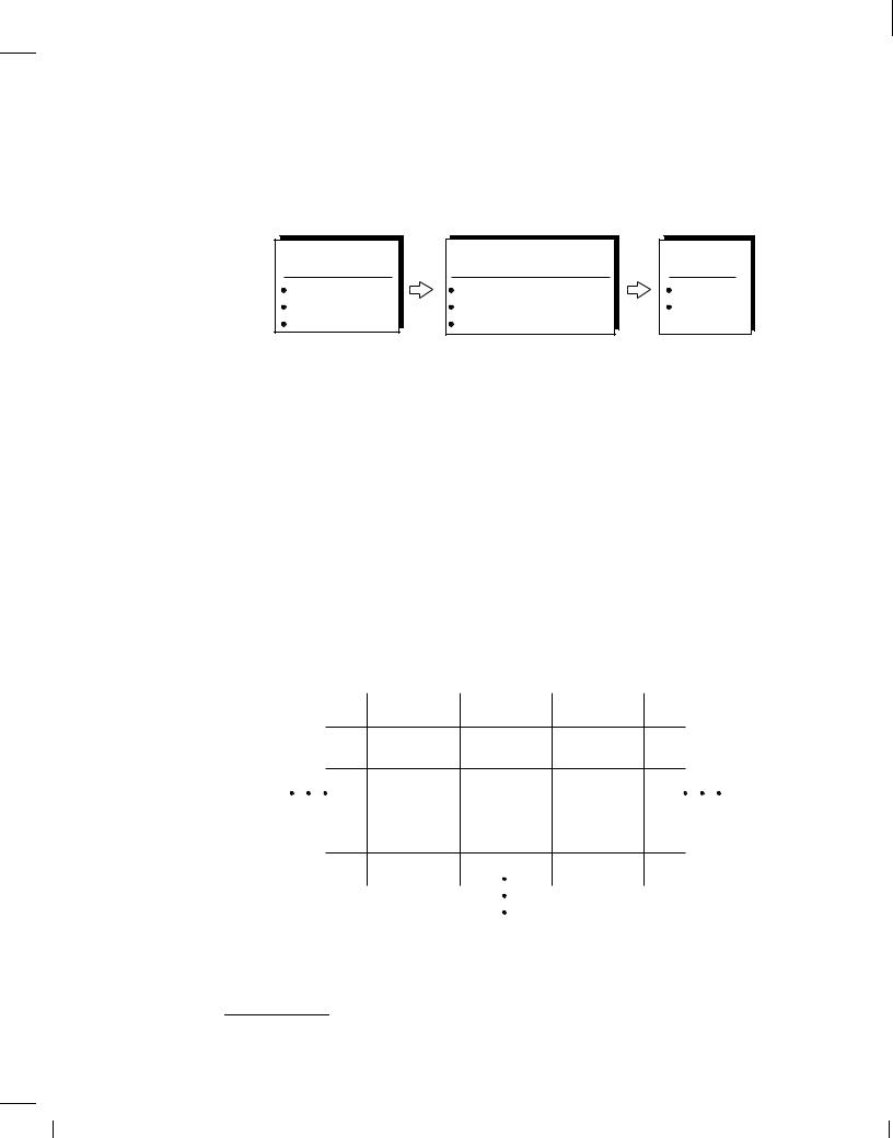
Figure 2.1 Outline of this section.
This outline represents a logical thought process: (a) we identify charge carriers in solids and formulate their role in current flow; (b) we examine means of modifying the density of charge carriers to create desired current flow properties; (c) we determine current flow mechanisms.
These steps naturally lead to the computation of the current/voltage (I/V) characteristics of actual diodes in the next section.
2.1.1 Charge Carriers in Solids
Recall from basic chemistry that the electrons in an atom orbit the nucleus in different “shells.” The atom's chemical activity is determined by the electrons in the outermost shell, called “valence” electrons, and how complete this shell is. For example, neon exhibits a complete outermost shell (with eight electrons) and hence no tendency for chemical reactions. On the other hand, sodium has only one valence electron, ready to relinquish it, and chloride has seven valence electrons, eager to receive one more. Both elements are therefore highly reactive.
The above principles suggest that atoms having approximately four valence electrons fall somewhere between inert gases and highly volatile elements, possibly displaying interesting chemical and physical properties. Shown in Fig. 2.2 is a section of the periodic table contain-
III |
IV |
V |
Boron Carbon
(B)(C)
Aluminum |
Silicon |
Phosphorous |
(Al) |
(Si) |
(P) |
|
|
|
Galium |
Germanium |
Arsenic |
(Ga) |
(Ge) |
(As) |
Figure 2.2 Section of the periodic table.
ing a number of elements with three to five valence electrons. As the most popular material in microelectronics, silicon merits a detailed analysis.2
2Silicon is obtained from sand after a great deal of processing.
BR |
Wiley/Razavi/Fundamentals of Microelectronics [Razavi.cls v. 2006] |
June 30, 2007 at 13:42 |
23 (1) |
|
|
|
|
Sec. 2.1 |
Semiconductor Materials and Their Properties |
23 |
Covalent Bonds A silicon atom residing in isolation contains four valence electrons [Fig. 2.3(a)], requiring another four to complete its outermost shell. If processed properly, the sili-
Covalent
Bond
|
Si |
|
Si |
Si |
Si |
|
Si |
Si |
Si |
Si |
Si |
Si e |
Si |
|
Si |
|
Si |
Si |
Si |
Free |
|
|
|
|
|
|
Electron |
(a) |
|
(b) |
|
|
(c) |
|
Figure 2.3 (a) Silicon atom, (b) covalent bonds between atoms, (c) free electron released by thermal energy.
con material can form a “crystal” wherein each atom is surrounded by exactly four others [Fig. 2.3(b)]. As a result, each atom shares one valence electron with its neighbors, thereby completing its own shell and those of the neighbors. The “bond” thus formed between atoms is called a “covalent bond” to emphasize the sharing of valence electrons.
The uniform crystal depicted in Fig. 2.3(b) plays a crucial role in semiconductor devices. But, does it carry current in response to a voltage? At temperatures near absolute zero, the valence electrons are confined to their respective covalent bonds, refusing to move freely. In other words, the silicon crystal behaves as an insulator for T ! 0K. However, at higher temperatures, electrons gain thermal energy, occasionally breaking away from the bonds and acting as free charge carriers [Fig. 2.3(c)] until they fall into another incomplete bond. We will hereafter use the term “electrons” to refer to free electrons.
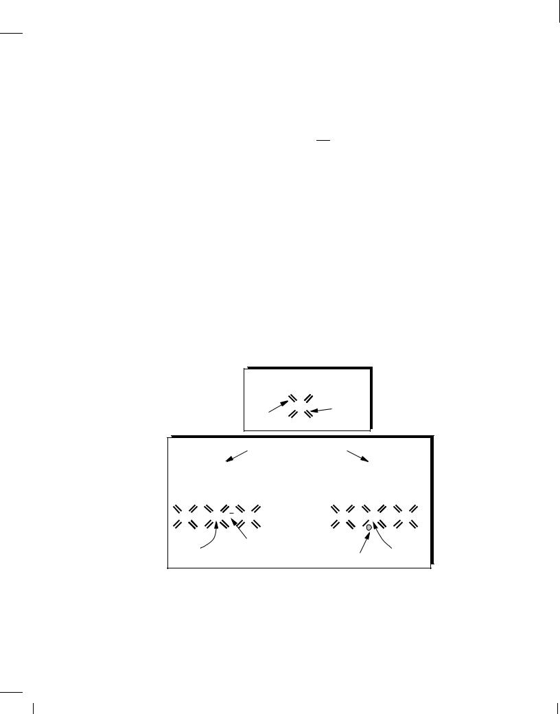
Holes When freed from a covalent bond, an electron leaves a “void” behind because the bond is now incomplete. Called a “hole,” such a void can readily absorb a free electron if one becomes available. Thus, we say an “electron-hole pair” is generated when an electron is freed, and an “electron-hole recombination” occurs when an electron “falls” into a hole.
Why do we bother with the concept of the hole? After all, it is the free electron that actually moves in the crystal. To appreciate the usefulness of holes, consider the time evolution illustrated in Fig. 2.4. Suppose covalent bond number 1 contains a hole after losing an electron some time
|
|
t = t1 |
|
|
t = t2 |
|
|
t = t3 |
|
|
1 |
Si |
|
Si |
Si |
|
Si |
Si |
|
Si |
3 |
|
|
|
|
|
|
|
|
|
||
Si |
|
Si |
Si |
Si |
Si |
Si |
Si |
Si |
|
Si |
|
Si |
|
Si |
Si |
2 |
Si |
Si |
|
Si |
|
|
|
|
|
|
Hole
Figure 2.4 Movement of electron through crystal.
before t = t1. At t = t2, an electron breaks away from bond number 2 and recombines with the hole in bond number 1. Similarly, at t = t3, an electron leaves bond number 3 and falls into the hole in bond number 2. Looking at the three “snapshots,” we can say one electron has traveled from right to left, or, alternatively, one hole has moved from left to right. This view of current flow by holes proves extremely useful in the analysis of semiconductor devices.
Bandgap Energy We must now answer two important questions. First, does any thermal energy create free electrons (and holes) in silicon? No, in fact, a minimum energy is required to

BR |
Wiley/Razavi/Fundamentals of Microelectronics [Razavi.cls v. 2006] |
June 30, 2007 at 13:42 |
24 (1) |
|
|
|
|
24 |
Chap. 2 |
Basic Physics of Semiconductors |
|
|
dislodge an electron from a covalent bond. Called the “bandgap energy” and denoted by |
Eg, this |
|
|
minimum is a fundamental property of the material. For silicon, Eg = 1:12 eV.3 |
|
|
|
The second question relates to the conductivity of the material and is as follows. How many |
||
|
free electrons are created at a given temperature? From our observations thus far, we postulate |
||
|
that the number of electrons depends on both Eg and T : a greater Eg translates to fewer electrons, |
||
|
but a higher T yields more electrons. To simplify future derivations, we consider the density (or |
||
|
concentration) of electrons, i.e., the number of electrons per unit volume, ni, and write for silicon: |
||
|
ni = 5:2 1015T3=2 exp ,Eg electrons=cm3 |
(2.1) |
|
|
2kT |
|
|
where k = 1:38 10,23 J/K is called the Boltzmann constant. The derivation can be found in books on semiconductor physics, e.g., [1]. As expected, materials having a larger Eg exhibit a smaller ni. Also, as T ! 0, so do T3=2 and exp[,Eg=(2kT )], thereby bringing ni toward zero.
The exponential dependence of ni upon Eg reveals the effect of the bandgap energy on the conductivity of the material. Insulators display a high Eg; for example, Eg = 2:5 eV for diamond. Conductors, on the other hand, have a small bandgap. Finally, semiconductors exhibit a moderate Eg, typically ranging from 1 eV to 1.5 eV.
Example 2.1
Determine the density of electrons in silicon at T = 300 K (room temperature) and T = 600 K.
Solution
Since Eg = 1:12 eV= 1:792 10,19 J, we have
n (T = 300 K) = 1:08 1010 |
electrons=cm3 |
(2.2) |
i |
|
|
n (T = 600 K) = 1:54 1015 |
electrons=cm3: |
(2.3) |
i |
|
|
Since for each free electron, a hole is left behind, the density of holes is also given by (2.2) and (2.3).
Exercise
Repeat the above exercise for a material having a bandgap of 1.5 eV.
The ni values obtained in the above example may appear quite high, but, noting that silicon has 5 1022 atoms=cm3, we recognize that only one in 5 1012 atoms benefit from a free electron at room temperature. In other words, silicon still seems a very poor conductor. But, do not despair! We next introduce a means of making silicon more useful.
2.1.2 Modification of Carrier Densities
Intrinsic and Extrinsic Semiconductors The “pure” type of silicon studied thus far is an example of “intrinsic semiconductors,” suffering from a very high resistance. Fortunately, it is possible to modify the resistivity of silicon by replacing some of the atoms in the crystal with atoms of another material. In an intrinsic semiconductor, the electron density, n(= ni), is equal
3The unit eV (electron volt) represents the energy necessary to move one electron across a potential difference of 1 V. Note that 1 eV= 1:6 10,19 J.
BR |
Wiley/Razavi/Fundamentals of Microelectronics [Razavi.cls v. 2006] |
June 30, 2007 at 13:42 |
25 (1) |
|
|
|
|
Sec. 2.1 Semiconductor Materials and Their Properties 25
to the hole density, p. Thus, |
|
|
np = n2 |
: |
(2.4) |
i |
|
|
We return to this equation later.
Recall from Fig. 2.2 that phosphorus (P) contains five valence electrons. What happens if some P atoms are introduced in a silicon crystal? As illustrated in Fig. 2.5, each P atom shares
Si Si
Si |
|
|
Si |
P e |
|||
Si Si
Figure 2.5 Loosely-attached electon with phosphorus doping.
four electrons with the neighboring silicon atoms, leaving the fifth electron “unattached.” This electron is free to move, serving as a charge carrier. Thus, if N phosphorus atoms are uniformly introduced in each cubic centimeter of a silicon crystal, then the density of free electrons rises by the same amount.
The controlled addition of an “impurity” such as phosphorus to an intrinsic semiconductor is called “doping,” and phosphorus itself a “dopant.” Providing many more free electrons than in the intrinsic state, the doped silicon crystal is now called “extrinsic,” more specifically, an “ n-type” semiconductor to emphasize the abundance of free electrons.
As remarked earlier, the electron and hole densities in an intrinsic semiconductor are equal. But, how about these densities in a doped material? It can be proved that even in this case,
np = n2; |
(2.5) |
i |
|
where n and p respectively denote the electron and hole densities in the extrinsic semiconductor. The quantity ni represents the densities in the intrinsic semiconductor (hence the subscript i) and is therefore independent of the doping level [e.g., Eq. (2.1) for silicon].
Example 2.2
The above result seems quite strange. How can np remain constant while we add more donor atoms and increase n?
Solution
Equation (2.5) reveals that p must fall below its intrinsic level as more n-type dopants are added to the crystal. This occurs because many of the new electrons donated by the dopant “recombine” with the holes that were created in the intrinsic material.
Exercise
Why can we not say that n + p should remain constant?
Example 2.3 
A piece of crystalline silicon is doped uniformly with phosphorus atoms. The doping density is
BR |
Wiley/Razavi/Fundamentals of Microelectronics [Razavi.cls v. 2006] |
June 30, 2007 at 13:42 |
26 (1) |
|
|
|
|
26 |
Chap. 2 |
Basic Physics of Semiconductors |
1016 atoms/cm3. Determine the electron and hole densities in this material at the room temperature.
Solution
The addition of 1016 P atoms introduces the same number of free electrons per cubic centimeter. Since this electron density exceeds that calculated in Example 2.1 by six orders of magnitude, we can assume
n = 1016 electrons=cm3 |
(2.6) |
|
It follows from (2.2) and (2.5) that |
|
|
p = |
n2 |
(2.7) |
i |
||
|
n |
|
= 1:17 104 holes=cm3 |
(2.8) |
|
Note that the hole density has dropped below the intrinsic level by six orders of magnitude. Thus, if a voltage is applied across this piece of silicon, the resulting current predominantly consists of electrons.
Exercise
At what doping level does the hole density drop by three orders of magnitude?
This example justifies the reason for calling electrons the “majority carriers” and holes the “minority carriers” in an n-type semiconductor. We may naturally wonder if it is possible to construct a “ p-type” semiconductor, thereby exchanging the roles of electrons and holes.
Indeed, if we can dope silicon with an atom that provides an insufficient number of electrons, then we may obtain many incomplete covalent bonds. For example, the table in Fig. 2.2 suggests that a boron (B) atom—with three valence electrons—can form only three complete covalent bonds in a silicon crystal (Fig. 2.6). As a result, the fourth bond contains a hole, ready to absorb
Si Si
Si |
B |
Si |
Si Si
Figure 2.6 Available hole with boron doping.
a free electron. In other words, N boron atoms contribute N boron holes to the conduction of current in silicon. The structure in Fig. 2.6 therefore exemplifies a p-type semiconductor, providing holes as majority carriers. The boron atom is called an “acceptor” dopant.
Let us formulate our results thus far. If an intrinsic semiconductor is doped with a density of ND ( ni) donor atoms per cubic centimeter, then the mobile charge densities are given by
Majority Carriers : n ND |
(2.9) |
||
|
n2 |
|
|
Minority Carriers : p |
i |
: |
(2.10) |
|
|||
|
ND |
|
|
BR |
Wiley/Razavi/Fundamentals of Microelectronics [Razavi.cls v. 2006] |
June 30, 2007 at 13:42 |
27 (1) |
|
|
|
|
Sec. 2.1 |
Semiconductor Materials and Their Properties |
|
27 |
|
Similarly, for a density of NA ( ni) acceptor atoms per cubic centimeter: |
|
|||
|
Majority Carriers : p NA |
|
(2.11) |
|
|
Minority Carriers : n |
ni2 |
: |
(2.12) |
|
|
NA |
|
|
Since typical doping densities fall in the range of 1015 to 1018 atoms=cm3, the above expressions are quite accurate.
Example 2.4 
Is it possible to use other elements of Fig. 2.2 as semiconductors and dopants?
Solution
Yes, for example, some early diodes and transistors were based on germanium (Ge) rather than silicon. Also, arsenic (As) is another common dopant.
Exercise
Can carbon be used for this purpose?
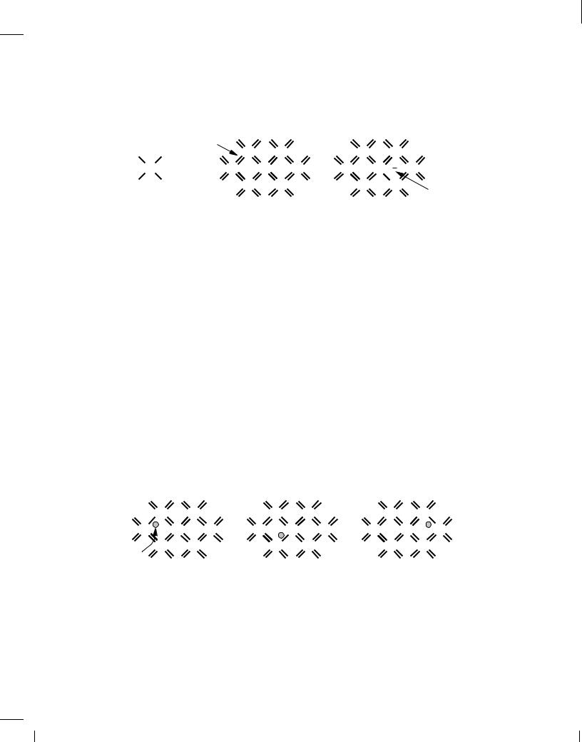
Figure 2.7 summarizes the concepts introduced in this section, illustrating the types of charge carriers and their densities in semiconductors.
|
|
Intrinsic Semiconductor |
|
|
|
|
|
Si |
|
|
|
|
|
Si |
Valence |
|
|
|
|
Covalent |
Electron |
|
|
|
|
Si |
|
|
|
|
|
Bond |
|
|
|
|
|
|
|
|
|
|
|
Extrinsic Semiconductor |
|
|
|
Silicon Crystal |
Silicon Crystal |
||||
ND Donors/cm3 |
NA Acceptors/cm3 |
||||
Si |
Si |
|
Si |
|
Si |
Si |
P e |
Si |
Si |
B |
Si |
Si |
Si |
Free |
Si |
|
Si |
n−Type |
|
|
|
p−Type |
|
Majority Carrier |
Free |
|
|||
Dopant |
|
Dopant |
|||
|
|
|
|||
(Donor) |
|
|
Majority Carrier |
(Acceptor) |
|
Figure 2.7 Summary of charge carriers in silicon.
2.1.3 Transport of Carriers
Having studied charge carriers and the concept of doping, we are ready to examine the movement of charge in semiconductors, i.e., the mechanisms leading to the flow of current.
BR |
Wiley/Razavi/Fundamentals of Microelectronics [Razavi.cls v. 2006] |
June 30, 2007 at 13:42 |
28 (1) |
|
|
|
|
28 Chap. 2 Basic Physics of Semiconductors
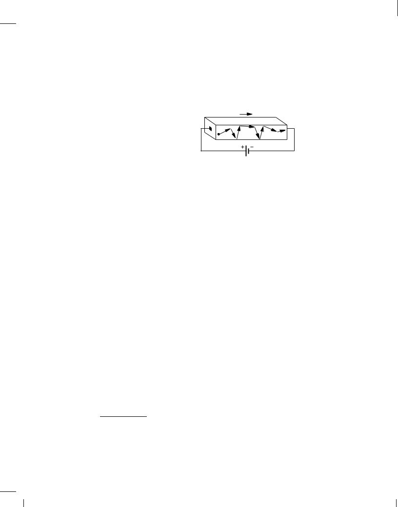
Drift We know from basic physics and Ohm's law that a material can conduct current in response to a potential difference and hence an electric field. 4 The field accelerates the charge carriers in the material, forcing some to flow from one end to the other. Movement of charge carriers due to an electric field is called “drift.” 5
Semiconductors behave in a similar manner. As shown in Fig. 2.8, the charge carriers are
E
Figure 2.8 Drift in a semiconductor.
accelerated by the field and accidentally collide with the atoms in the crystal, eventually reaching the other end and flowing into the battery. The acceleration due to the field and the collision with the crystal counteract, leading to a constant velocity for the carriers.6 We expect the velocity, v, to be proportional to the electric field strength, E:
v / E; |
(2.13) |
and hence |
|
v = E; |
(2.14) |
where is called the “mobility” and usually expressed in |
cm2=(V s). For example in silicon, |
the mobility of electrons, n = 1350 cm2=(V s), and that of holes, p = 480 cm2=(V s). Of course, since electrons move in a direction opposite to the electric field, we must express the velocity vector as
! |
|
! |
(2.15) |
|
|
||
ve |
= , n E : |
||
For holes, on the other hand, |
|
|
|
! |
! |
(2.16) |
|
|
|||
vh= p E : |
|||
Example 2.5
A uniform piece of n-type of silicon that is 1 m long senses a voltage of 1 V. Determine the velocity of the electrons.
Solution
Since the material is uniform, we have E = V=L, where L is the length. Thus, E = 10; 000 V/cm and hence v = nE = 1:35 107 cm/s. In other words, electrons take (1 m)=(1:35 107 cm=s) = 7:4 ps to cross the 1- m length.
4Recall that the potential (voltage) difference, V , is equal to the negative integral of the electric field, E, with respect to distance: Vab = ,Rba Edx.
5The convention for direction of current assumes flow of positive charge from a positive voltage to a negative voltage. Thus, if electrons flow from point A to point B, the current is considered to have a direction from B to A.
6This phenomenon is analogous to the “terminal velocity” that a sky diver with a parachute (hopefully, open) experiences.
BR |
Wiley/Razavi/Fundamentals of Microelectronics [Razavi.cls v. 2006] |
June 30, 2007 at 13:42 |
29 (1) |
|
|
|
|
Sec. 2.1 |
Semiconductor Materials and Their Properties |
29 |
Exercise
What happens if the mobility is halved?
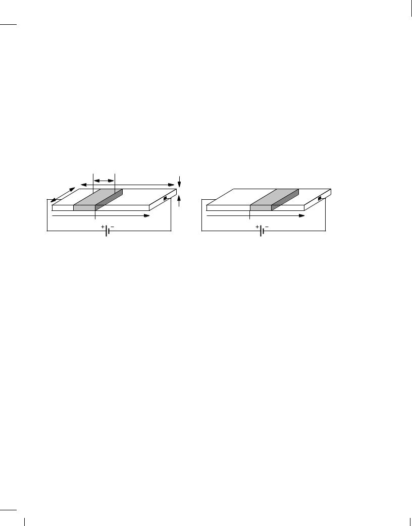
With the velocity of carriers known, how is the current calculated? We first note that an electron carries a negative charge equal to q = 1:6 10,19 C. Equivalently, a hole carries a positive charge of the same value. Now suppose a voltage V1 is applied across a uniform semiconductor bar having a free electron density of n (Fig. 2.9). Assuming the electrons move with a velocity of
v |
t = t1 |
t = t1 + 1 s |
meters |
L |
|
|
|
|
W |
|
h |
x 1 |
x |
x |
|
x 1 |
|
V1 |
|
V1 |
Figure 2.9 Current flow in terms of charge density.
v m/s, considering a cross section of the bar at x = x1 and taking two “snapshots” at t = t1 and t = t1 + 1 second, we note that the total charge in v meters passes the cross section in 1 second. In other words, the current is equal to the total charge enclosed in v meters of the bar's length. Since the bar has a width of W , we have:
I = ,v W h n q; |
(2.17) |
where v W h represents the volume, n q denotes the charge density in coulombs, and the negative sign accounts for the fact that electrons carry negative charge.
Let us now reduce Eq. (2.17) to a more convenient form. Since for electrons, v = , nE, and since W h is the cross section area of the bar, we write
Jn = nE n q; |
(2.18) |
where Jn denotes the “current density,” i.e., the current passing through a unit cross section area, and is expressed in A=cm2. We may loosely say, “the current is equal to the charge velocity times the charge density,” with the understanding that “current” in fact refers to current density, and negative or positive signs are taken into account properly.
In the presence of both electrons and holes, Eq. (2.18) is modified to
Jtot = nE n q + pE p q |
(2.19) |
= q( nn + pp)E: |
(2.20) |
This equation gives the drift current density in response to an electric field E in a semiconductor having uniform electron and hole densities.
BR |
Wiley/Razavi/Fundamentals of Microelectronics [Razavi.cls v. 2006] |
June 30, 2007 at 13:42 |
30 (1) |
|
|
|
|
30 |
Chap. 2 |
Basic Physics of Semiconductors |
Example 2.6
In an experiment, it is desired to obtain equal electron and hole drift currents. How should the carrier densities be chosen?
Solution
We must impose |
|
|
|
|
|
|
|
|
nn = pp; |
(2.21) |
|||||||
and hence |
|
|
|
|
|
|
|
|
n = |
|
|
p : |
(2.22) |
||||
p |
|
|
n |
|
||||
We also recall that np = n2. Thus, |
|
|
|
|
|
|
|
|
i |
|
|
|
|
|
|
|
|
p = r |
|
|
|
|
ni |
|
||
|
n |
(2.23) |
||||||
|
|
|
|
|||||
|
|
|
|
p |
|
|||
|
|
|
ni: |
|
||||
n = r |
p |
(2.24) |
||||||
|
|
n |
|
|||||
For example, in silicon, n= p = 1350=480 = 2:81, yielding |
|
|||||||
p = 1:68ni |
(2.25) |
|||||||
n = 0:596ni: |
(2.26) |
|||||||
Since p and n are of the same order as ni, equal electron and hole drift currents can occur for only a very lightly doped material. This confirms our earlier notion of majority carriers in semiconductors having typical doping levels of 1015-1018 atoms=cm3.
Exercise
How should the carrier densities be chosen so that the electron drift current is twice the hole drift current?
Velocity Saturation We have thus far assumed that the mobility of carriers in semiconductors is independent of the electric field and the velocity rises linearly with E according to v = E. In reality, if the electric field approaches sufficiently high levels, v no longer follows E linearly. This is because the carriers collide with the lattice so frequently and the time between the collisions is so short that they cannot accelerate much. As a result, v varies “sublinearly” at high electric fields, eventually reaching a saturated level, vsat (Fig. 2.10). Called “velocity saturation,” this effect manifests itself in some modern transistors, limiting the performance of circuits.
In order to represent velocity saturation, we must modify v = E accordingly. A simple approach is to view the slope, , as a field-dependent parameter. The expression for must
This section can be skipped in a first reading.