

Fundamentals of Microelectronics
.pdfBR |
Wiley/Razavi/Fundamentals of Microelectronics [Razavi.cls v. 2006] |
June 30, 2007 at 13:42 |
31 (1) |
|
|
|
|
Sec. 2.1 |
Semiconductor Materials and Their Properties |
31 |
Velocity
vsat
 2
2  1
1
E
Figure 2.10 Velocity saturation.
therefore gradually fall toward zero as E rises, but approach a constant value for small E; i.e.,
= |
0 |
; |
(2.27) |
|
1 + bE |
||||
|
|
|
where 0 is the “low-field” mobility and b a proportionality factor. We may consider as the “effective” mobility at an electric field E. Thus,
v = |
|
0 |
E: |
(2.28) |
||||
1 + bE |
||||||||
|
|
|
|
|
||||
Since for E ! 1, v ! vsat, we have |
|
|
|
|
|
|
||
v |
|
= 0 |
; |
|
(2.29) |
|||
sat |
|
b |
|
|
|
|||
|
|
|
|
|
|
|
||
and hence b = 0=vsat. In other words, |
|
|
|
|
|
|
||
v = |
|
|
0 |
|
E: |
(2.30) |
||
|
|
|
0E |
|||||
1 + |
vsat |
|
||||||
|
|
|
|
|
||||
Example 2.7
A uniform piece of semiconductor 0.2 m long sustains a voltage of 1 V. If the low-field mobility is equal to 1350 cm2=(V s) and the saturation velocity of the carriers 107 cm/s, determine the effective mobility. Also, calculate the maximum allowable voltage such that the effective mobility is only 10% lower than 0.
Solution
We have
E = VL
= 50 kV=cm:
It follows that
= |
0 |
||
1 + |
0E |
||
|
|||
|
|
vsat |
|
= |
0 |
|
|
7:75 |
|
||
|
|
||
= 174 cm2=(V s):
(2.31)
(2.32)
(2.33)
(2.34)
(2.35)
BR |
Wiley/Razavi/Fundamentals of Microelectronics [Razavi.cls v. 2006] |
June 30, 2007 at 13:42 |
32 (1) |
|
|
|
|
32 Chap. 2 Basic Physics of Semiconductors
If the mobility must remain within 10% of its low-field value, then
0:9 0 = |
0 |
; |
(2.36) |
|||
1 + |
0 E |
|||||
|
|
|
|
|||
|
|
|
vsat |
|
|
|
and hence |
|
|
|
|
|
|
E = |
1 vsat |
|
|
(2.37) |
||
|
9 0 |
|
|
|
||
= 823 V=cm: |
|
(2.38) |
||||
A device of length 0.2 m experiences such a field if it sustains a voltage of |
(823 V=cm) (0:2 |
|||||
10,4 cm) = 16:5 mV. |
|
|
|
|
|
|
This example suggests that modern (submicron) devices incur substantial velocity saturation because they operate with voltages much greater than 16.5 mV.
Exercise
At what voltage does the mobility fall by 20%?
Diffusion In addition to drift, another mechanism can lead to current flow. Suppose a drop of ink falls into a glass of water. Introducing a high local concentration of ink molecules, the drop begins to “diffuse,” that is, the ink molecules tend to flow from a region of high concentration to regions of low concentration. This mechanism is called “diffusion.”
A similar phenomenon occurs if charge carriers are “dropped” (injected) into a semiconductor so as to create a nonuniform density. Even in the absence of an electric field, the carriers move toward regions of low concentration, thereby carrying an electric current so long as the nonuniformity is sustained. Diffusion is therefore distinctly different from drift.
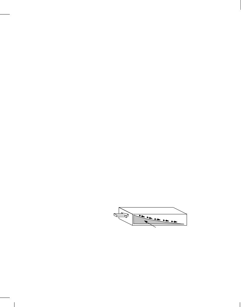
Figure 2.11 conceptually illustrates the process of diffusion. A source on the left continues to inject charge carriers into the semiconductor, a nonuniform charge profile is created along the x-axis, and the carriers continue to “roll down” the profile.
Semiconductor Material
Injection
of Carriers
Nonuniform Concentration
Figure 2.11 Diffusion in a semiconductor.
The reader may raise several questions at this point. What serves as the source of carriers in Fig. 2.11? Where do the charge carriers go after they roll down to the end of the profile at the far right? And, most importantly, why should we care?! Well, patience is a virtue and we will answer these questions in the next section.
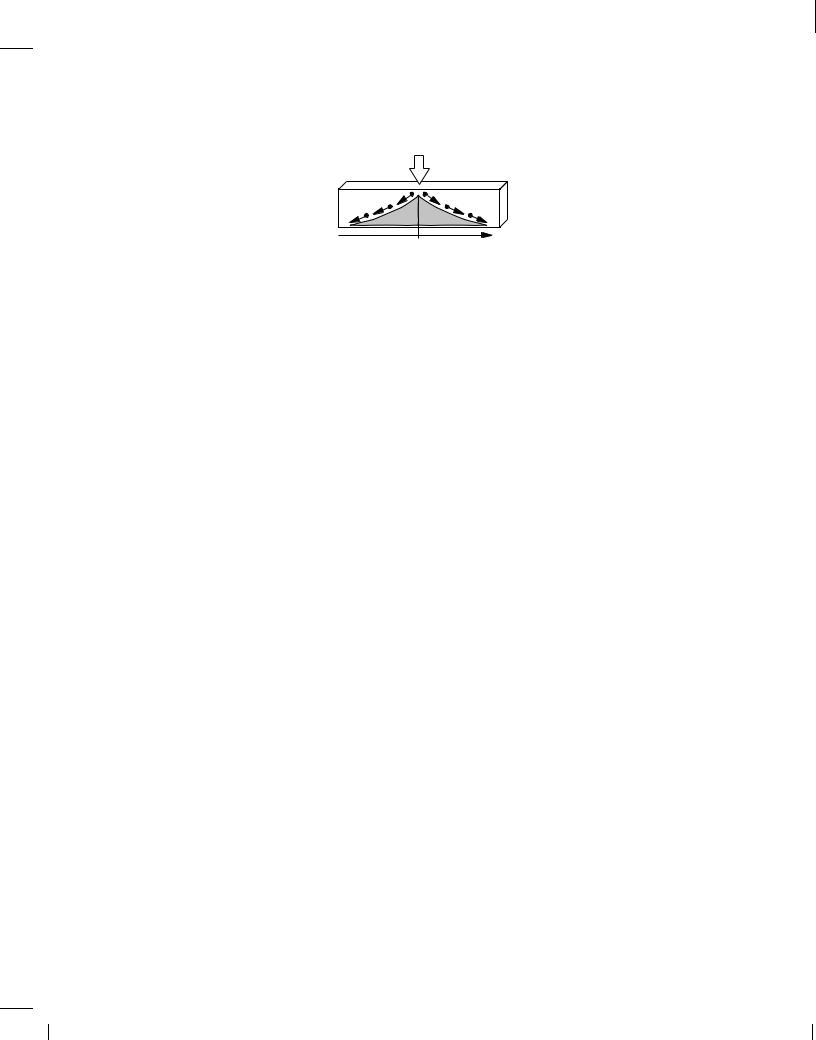
Example 2.8
A source injects charge carriers into a semiconductor bar as shown in Fig. 2.12. Explain how the current flows.
BR |
Wiley/Razavi/Fundamentals of Microelectronics [Razavi.cls v. 2006] |
June 30, 2007 at 13:42 |
33 (1) |
|
|
|
|
Sec. 2.1 |
Semiconductor Materials and Their Properties |
33 |
Injection
of Carriers
0 x
Figure 2.12 Injection of carriers into a semiconductor.
Solution
In this case, two symmetric profiles may develop in both positive and negative directions along the x-axis, leading to current flow from the source toward the two ends of the bar.
Exercise
Is KCL still satisfied at the point of injection?
Our qualitative study of diffusion suggests that the more nonuniform the concentration, the larger the current. More specifically, we can write:
I / dn |
; |
(2.39) |
dx |
|
|
where n denotes the carrier concentration at a given point along the x-axis. We call dn=dx the concentration “gradient” with respect to x, assuming current flow only in the x direction. If each carrier has a charge equal to q, and the semiconductor has a cross section area of A, Eq. (2.39) can be written as
I / Aq dn: |
|
(2.40) |
dx |
|
|
Thus, |
|
|
I = AqD dn |
; |
(2.41) |
n dx |
|
|
where Dn is a proportionality factor called the “diffusion constant” and expressed in |
cm2=s. For |
|
example, in intrinsic silicon, Dn = 34 cm2=s (for electrons), and Dp = 12 cm2=s (for holes). As with the convention used for the drift current, we normalize the diffusion current to the
cross section area, obtaining the current density as |
|
|
|
Jn = qDn dn |
: |
|
(2.42) |
dx |
|
|
|
Similarly, a gradient in hole concentration yields: |
|
|
|
Jp = ,qDp dp |
: |
(2.43) |
|
dx |
|
|
|
BR |
Wiley/Razavi/Fundamentals of Microelectronics [Razavi.cls v. 2006] |
June 30, 2007 at 13:42 |
34 (1) |
|
|
|
|
34 Chap. 2 Basic Physics of Semiconductors
With both electron and hole concentration gradients present, the total current density is given by
J |
= q D dn |
, D |
dp |
: |
(2.44) |
tot |
n dx |
|
p dx |
|
|
Example 2.9
Consider the scenario depicted in Fig. 2.11 again. Suppose the electron concentration is equal to N at x = 0 and falls linearly to zero at x = L (Fig. 2.13). Determine the diffusion current.
N |
|
|
Injection |
|
|
0 |
L |
x |
Figure 2.13 Current resulting from a linear diffusion profile.
Solution
We have
J |
= qD |
dn |
|
|
(2.45) |
n |
|
n dx |
|
|
|
|
= ,qDn |
N |
: |
(2.46) |
|
|
|
|
L |
|
|
The current is constant along the x-axis; i.e., all of the electrons entering the material at x = 0 successfully reach the point at x = L. While obvious, this observation prepares us for the next example.
Exercise
Repeat the above example for holes.
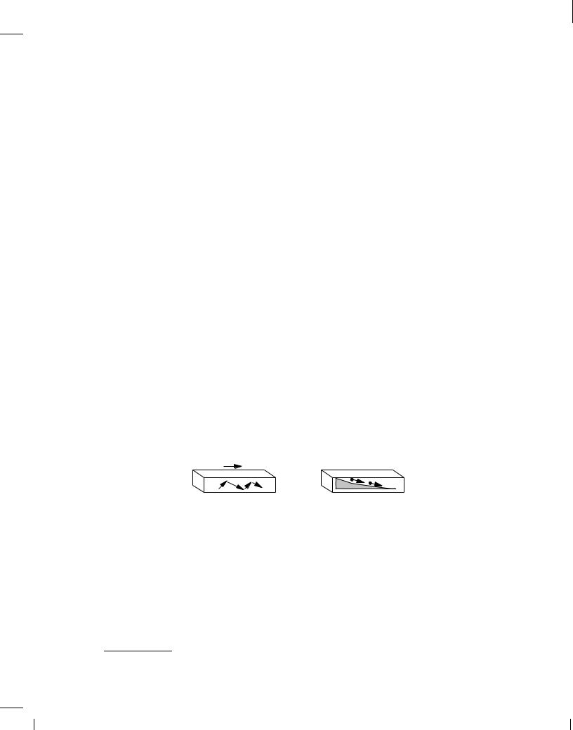
Example 2.10
Repeat the above example but assume an exponential gradient (Fig. 2.14):
N
Injection
0 |
L x |
Figure 2.14 Current resulting from an exponential diffusion profile.
n(x) = N exp ,x; |
(2.47) |
Ld |
|
BR |
Wiley/Razavi/Fundamentals of Microelectronics [Razavi.cls v. 2006] |
June 30, 2007 at 13:42 |
35 (1) |
|
|
|
|
Sec. 2.2 |
P N Junction |
35 |
where Ld is a constant.7
Solution
We have
J |
= qD |
dn |
|
(2.48) |
n |
|
n dx |
|
|
|
= ,qDnN exp ,x : |
(2.49) |
||
|
|
Ld |
Ld |
|
Interestingly, the current is not constant along the x-axis. That is, some electrons vanish while traveling from x = 0 to the right. What happens to these electrons? Does this example violate the law of conservation of charge? These are important questions and will be answered in the next section.
Exercise
At what value of x does the current density drop to 1% its maximum value?
Einstein Relation Our study of drift and diffusion has introduced a factor for each: n (orp) and Dn (or Dp), respectively. It can be proved that and D are related as:
D |
= kT |
: |
(2.50) |
|
q |
|
|
Called the “Einstein Relation,” this result is proved in semiconductor physics texts, e.g., [1]. Note that kT=q 26 mV at T = 300 K.
Figure 2.15 summarizes the charge transport mechanisms studied in this section.
Drift Current
E
Jn = q n n E
Jp = q p p E
Figure 2.15 Summary of drift and diffusion mechanisms.
Diffusion Current
Jn = q Dn |
dn |
|||
dx |
||||
|
|
|||
Jp = |
− q Dp |
dp |
||
|
||||
dx |
||||
|
|
|
||
2.2 PN Junction
We begin our study of semiconductor devices with the pn junction for three reasons. (1) The device finds application in many electronic systems, e.g., in adapters that charge the batteries of cellphones. (2) The pn junction is among the simplest semiconductor devices, thus providing a
7The factor Ld is necessary to convert the exponent to a dimensionless quantity.
BR |
Wiley/Razavi/Fundamentals of Microelectronics [Razavi.cls v. 2006] |
June 30, 2007 at 13:42 |
36 (1) |
|
|
|
|
36 |
Chap. 2 |
Basic Physics of Semiconductors |
good entry point into the study of the operation of such complex structures as transistors. (3) The pn junction also serves as part of transistors. We also use the term “diode” to refer to pn junctions.
We have thus far seen that doping produces free electrons or holes in a semiconductor, and an electric field or a concentration gradient leads to the movement of these charge carriers. An interesting situation arises if we introduce n-type and p-type dopants into two adjacent sections of a piece of semiconductor. Depicted in Fig. 2.16 and called a “ pn junction,” this structure plays a fundamental role in many semiconductor devices. The p and n sides are called the “anode” and
|
n |
p |
|
|
|
|
|
Cathode |
Anode |
Si |
Si |
Si |
Si |
|
P |
e |
|
B |
|
Si |
Si |
Si |
Si |
|
|
(a) |
|
|
(b) |
Figure 2.16 PN junction.
the ”cathode,” respectively.
In this section, we study the properties and I/V characteristics of pn junctions. The following outline shows our thought process, indicating that our objective is to develop circuit models that can be used in analysis and design.
|
|
|
|
|
|
|
|
|
|
|
|
|
PN Junction |
|
|
PN Junction |
|
|
|
PN Junction |
|
||
|
in Equilibrium |
|
|
Under Reverse Bias |
|
|
|
Under Forward Bias |
|
||
|
|
|
|
|
|
|
|
|
|
|
|
|
Depletion Region |
|
|
Junction Capacitance |
|
|
|
I/V Characteristics |
|
||
|
Built−in Potential |
|
|
|
|
|
|
|
|
|
|
|
|
|
|
|
|
|
|
|
|
|
|
|
|
|
|
|
|
|
|
|
|
|
|
Figure 2.17 Outline of concepts to be studied.
2.2.1 P N Junction in Equilibrium
Let us first study the pn junction with no external connections, i.e., the terminals are open and no voltage is applied across the device. We say the junction is in “equilibrium.” While seemingly of no practical value, this condition provides insights that prove useful in understanding the operation under nonequilibrium as well.
We begin by examining the interface between the n and p sections, recognizing that one side contains a large excess of holes and the other, a large excess of electrons. The sharp concentration gradient for both electrons and holes across the junction leads to two large diffusion currents: electrons flow from the n side to the p side, and holes flow in the opposite direction. Since we must deal with both electron and hole concentrations on each side of the junction, we introduce the notations shown in Fig. 2.18.
Example 2.11
A pn junction employs the following doping levels: NA = 1016 cm,3 and ND = 5 1015 cm,3. Determine the hole and electron concentrations on the two sides.
Solution
From Eqs. (2.11) and (2.12), we express the concentrations of holes and electrons on the p side
BR |
Wiley/Razavi/Fundamentals of Microelectronics [Razavi.cls v. 2006] |
June 30, 2007 at 13:42 |
37 (1) |
|
|
|
|
Sec. 2.2 |
P N Junction |
|
|
|
|
|
|
|
|
Majority |
|
n |
p |
Majority |
|
|
|
|
|
|
|
||
|
|
|
|
|
|
||
|
|
Carriers |
n |
|
pp |
|
Carriers |
|
|
|
n |
|
|
||
|
|
|
|
|
|
|
|
|
|
Minority |
p |
n |
np |
|
Minority |
|
|
|
|
|
|||
|
|
Carriers |
|
|
|
|
Carriers |
|
|
|
|
|
|
||
|
|
nn : Concentration of electrons on n side |
|
||||
|
|
pn : Concentration of holes on n side |
|
||||
|
|
pp : Concentration of holes on p side |
|
||||
Figure 2.18 |
. |
np : Concentration of electrons on p side |
|
||||
respectively as:
pp NA
= 1016 cm,3
n2
np NiA
= (1:08 1010 cm,3)2 1016 cm,3
1:1 104 cm,3:
Similarly, the concentrations on the n side are given by
nn ND
= 5 1015 cm,3
n2 pn Ni
D
=(1:08 1010 cm,3)2 5 1015 cm,3
=2:3 104 cm,3:
37
(2.51)
(2.52)
(2.53)
(2.54)
(2.55)
(2.56)
(2.57)
(2.58)
(2.59)
(2.60)
Note that the majority carrier concentration on each side is many orders of magnitude higher than the minority carrier concentration on either side.
Exercise
Repeat the above example if ND drops by a factor of four.
The diffusion currents transport a great deal of charge from each side to the other, but they must eventually decay to zero. This is because, if the terminals are left open (equilibrium condition), the device cannot carry a net current indefinitely.
We must now answer an important question: what stops the diffusion currents? We may postulate that the currents stop after enough free carriers have moved across the junction so as to equalize the concentrations on the two sides. However, another effect dominates the situation and stops the diffusion currents well before this point is reached.
BR |
Wiley/Razavi/Fundamentals of Microelectronics [Razavi.cls v. 2006] |
June 30, 2007 at 13:42 |
38 (1) |
|
|
|
|
38 |
Chap. 2 |
Basic Physics of Semiconductors |
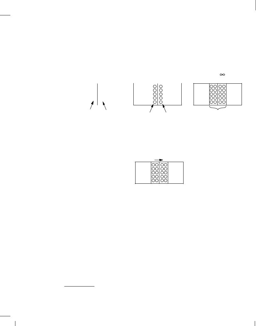
To understand this effect, we recognize that for every electron that departs from the n side, a positive ion is left behind, i.e., the junction evolves with time as conceptually shown in Fig. 2.19. In this illustration, the junction is suddenly formed at t = 0, and the diffusion currents continue to expose more ions as time progresses. Consequently, the immediate vicinity of the junction is depleted of free carriers and hence called the “depletion region.”
t = 0 |
t = t1 |
|
|
|
|
n |
|
|
|
|
|
|
|
p |
|
|
|
|
|
|
− |
|
− |
|
− |
|
− |
|
+ |
+ |
+ |
+ |
|
|
|||
− |
− |
− |
− |
− |
− |
− |
− |
− |
+ |
+ |
+ |
+ |
+ |
+ |
+ |
+ |
+ |
− |
− |
− |
− |
− |
− |
− |
− |
− |
+ |
+ |
+ |
+ |
+ |
+ |
+ |
+ |
+ |
− |
− |
− |
− |
− |
+ |
+ |
+ |
+ |
+ |
||||||||
− |
− |
− |
− |
− |
− |
− |
− |
− |
+ |
+ |
+ |
+ |
+ |
+ |
+ |
+ |
+ |
|
|
|
|
|
|
|
|
|
|
|
|
||||||
|
|
|
|
|
Free |
|
Free |
|
|
|
|
||||||
|
|
|
Electrons |
|
Holes |
|
|
|
|
||||||||
|
|
|
|
n |
|
|
|
|
|
p |
|
|
|
|
||
− |
− |
− |
− |
− |
− |
− |
+ |
− |
+ |
|
+ |
|
+ |
|
+ |
|
− |
− |
− |
+ |
− |
+ |
+ |
+ |
+ |
+ |
+ |
||||||
− |
− |
− |
− |
+ |
+ |
+ |
+ |
|||||||||
− |
− |
− |
+ − |
+ |
+ |
+ |
||||||||||
−−− −− − + − +++++++
−− − − + − + + + +−
Positive Negative
Donor Acceptor
Ions Ions
Figure 2.19 Evolution of charge concentrations in a pn junction.
|
|
|
|
|
|
t = |
|
|
|
|
|
|
|
|
|
|
n |
|
|
p |
|
|
|
|
|
|
− |
|
− |
|
− |
+ + − −+ |
|
+ |
|
+ |
|
|
− |
− |
− |
− |
− |
− + + − − + |
+ |
+ |
+ |
+ |
+ |
||
− |
− |
− |
− |
− |
− |
+ + − − + |
+ |
+ |
+ |
+ |
+ |
|
− |
− |
− |
− |
− |
− |
+ + − − |
+ |
+ |
+ |
+ |
+ |
+ |
− |
|
− |
|
− |
|
+ + − − |
|
+ |
|
+ |
|
+ |
Depletion
Region
Now recall from basic physics that a particle or object carrying a net (nonzero) charge creates an electric field around it. Thus, with the formation of the depletion region, an electric field emerges as shown in Fig. 2.20.8 Interestingly, the field tends to force positive charge flow from
|
|
|
|
n |
|
E |
|
|
p |
|
|
|
|
− |
|
− |
|
− |
+ + − −+ |
|
+ |
|
+ |
|
|
− |
− |
− |
− |
− |
− + + − − + |
+ |
+ |
+ |
+ |
+ |
||
− |
− |
− |
− |
− |
− |
+ + − − + |
+ |
+ |
+ |
+ |
+ |
|
− |
− |
− |
− |
− |
− |
+ + − − |
+ |
+ |
+ |
+ |
+ |
+ |
− |
|
− |
|
− |
|
+ + − − |
|
+ |
|
+ |
|
+ |
Figure 2.20 Electric field in a pn junction.
left to right whereas the concentration gradients necessitate the flow of holes from right to left (and electrons from left to right). We therefore surmise that the junction reaches equilibrium once the electric field is strong enough to completely stop the diffusion currents. Alternatively, we can say, in equilibrium, the drift currents resulting from the electric field exactly cancel the diffusion currents due to the gradients.
Example 2.12
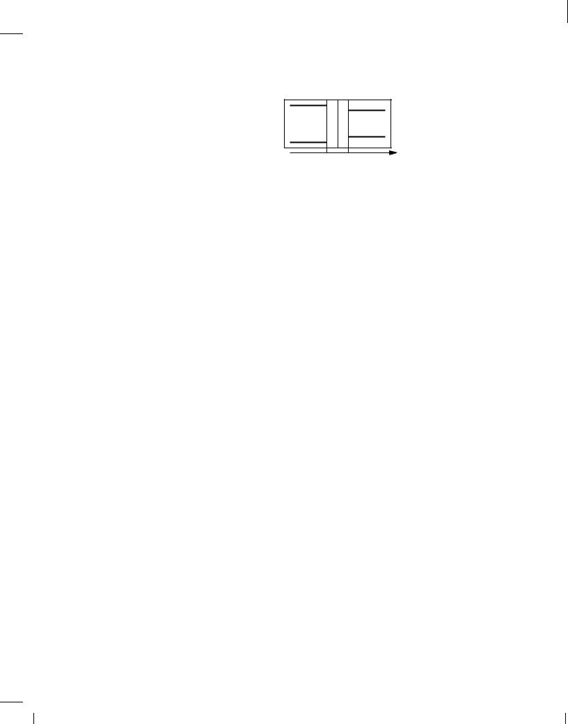
In the junction shown in Fig. 2.21, the depletion region has a width of b on the n side and a on the p side. Sketch the electric field as a function of x.
Solution
Beginning at x < ,b, we note that the absence of net charge yields E = 0. At x > ,b, each positive donor ion contributes to the electric field, i.e., the magnitude of E rises as x approaches zero. As we pass x = 0, the negative acceptor atoms begin to contribute negatively to the field, i.e., E falls. At x = a, the negative and positive charge exactly cancel each other and E = 0.
8The direction of the electric field is determined by placing a small positive test charge in the region and watching how it moves: away from positive charge and toward negative charge.

BR |
Wiley/Razavi/Fundamentals of Microelectronics [Razavi.cls v. 2006] |
June 30, 2007 at 13:42 |
39 (1) |
|
|
|
|
Sec. 2.2 |
P N Junction |
|
|
|
|
|
|
|
|
|
|
|
|
|
|
39 |
||
|
|
|
|
|
n |
|
|
|
|
E |
|
|
p |
|
|
|
|
|
|
|
|
|
|
|
|
|
|
|
|
|
|
|
|
|
|
||
|
|
|
|
|
|
|
|
|
|
|
|
|
|
|
|
|
||
|
|
|
|
|
|
|
|
|
|
|
|
|
|
|
|
|
|
|
|
|
|
− |
|
− |
|
|
− |
+ + |
− |
− + |
+ |
|
+ |
|
|
||
|
|
− |
− |
− |
− |
− |
|
− + + − − + |
+ |
+ |
+ |
+ |
+ |
|
||||
|
|
− |
− N D− |
− |
+ + − − + |
N A |
+ |
+ |
|
|||||||||
|
|
− |
− |
− |
− |
− |
− |
+ + − − + |
+ |
+ |
+ |
+ |
+ |
|
||||
|
|
− |
|
− |
|
− |
|
|
+ + |
− |
− |
+ |
|
+ |
|
+ |
|
|
|
|
|
|
|
|
|
|
|
|
|
|
|
|
|
|
|
|
|
|
|
|
|
|
|
|
|
|
− b |
0 |
a |
|
|
|
|
x |
||
|
|
|
|
|
|
|
|
|
E |
|
|
|
|
|
|
|
|
|
|
|
|
|
|
|
|
|
|
|
|
|
|
|
|
|
|
|
|
|
|
|
|
|
|
|
|
|
− b |
0 |
a |
|
|
|
|
x |
||
Figure 2.21 |
Electric field profile in a pn junction. |
|
|
|
|
|
|
|
|
|
|
|
|
|
|
|||
Exercise
Noting that potential voltage is negative integral of electric field with respect to distance, plot the potential as a function of x.
From our observation regarding the drift and diffusion currents under equilibrium, we may be tempted to write:
jIdrift;p + Idrift;nj = jIdi ;p + Idi ;nj; |
(2.61) |
where the subscripts p and n refer to holes and electrons, respectively, and each current term contains the proper polarity. This condition, however, allows an unrealistic phenomenon: if the number of the electrons flowing from the n side to the p side is equal to that of the holes going from the p side to the n side, then each side of this equation is zero while electrons continue to accumulate on the p side and holes on the n side. We must therefore impose the equilibrium condition on each carrier:
jIdrift;pj = jIdi ;pj |
(2.62) |
jIdrift;nj = jIdi ;nj: |
(2.63) |
Built-in Potential The existence of an electric field within the depletion region suggests that the junction may exhibit a “built-in potential.” In fact, using (2.62) or (2.63), we can compute this potential. Since the electric field E = ,dV=dx, and since (2.62) can be written as
q pE = qD |
|
|
dp ; |
|
|
|
(2.64) |
||
p |
|
|
p dx |
|
|
|
|
||
we have |
|
|
|
|
|
|
|
|
|
, p dV |
= D |
|
dp |
: |
|
|
(2.65) |
||
p |
dx |
|
|
p dx |
|
|
|
|
|
Dividing both sides by p and taking the integral, we obtain |
|
|
|
||||||
x2 |
dV = D |
|
|
pp |
dp |
; |
(2.66) |
||
, Z |
p |
Z |
|
|
|||||
p |
|
|
|
|
p |
|
|
||
x1 |
|
|
|
|
pn |
|
|
|
|
BR |
Wiley/Razavi/Fundamentals of Microelectronics [Razavi.cls v. 2006] |
June 30, 2007 at 13:42 |
40 (1) |
|
|
|
|
40 |
Chap. 2 |
Basic Physics of Semiconductors |
n |
|
p |
nn
pn
pp
np
x 1 x 2 |
x |
Figure 2.22 Carrier profiles in a pn junction.
where pn and pp are the hole concentrations at x1 and x2, respectively (Fig. 2.22). Thus,
V (x2) , V (x1) = ,Dp ln |
pp : |
(2.67) |
p |
pn |
|
The right side represents the voltage difference developed across the depletion region and will be denoted by V0. Also, from Einstein's relation, Eq. (2.50), we can replace Dp= p with kT=q:
jV0j = kT |
ln pp : |
(2.68) |
q |
pn |
|
Exercise
Writing Eq. (2.64) for electron drift and diffusion currents, and carrying out the integration, derive an equation for V0 in terms of nn and np.
Finally, using (2.11) and (2.10) for pp and pn yields
V0 |
= kT ln |
NAND |
: |
(2.69) |
|
q |
n2 |
|
|
|
|
i |
|
|
Expressing the built-in potential in terms of junction parameters, this equation plays a central role in many semiconductor devices.
Example 2.13 
A silicon pn junction employs NA = 2 1016 cm,3 and ND = 4 1016 cm,3. Determine the built-in potential at room temperature (T = 300 K).
Solution
Recall from Example 2.1 that ni(T = 300 K) = 1:08 1010 cm,3. Thus,
V0 |
(26 mV) ln |
(2 |
1016) (4 1016) |
(2.70) |
|
768 mV: |
|
(1:08 1010)2 |
(2.71) |
|
|
|
Exercise
By what factor should ND be changed to lower V0 by 20 mV?