

Fundamentals of Microelectronics
.pdfBR |
Wiley/Razavi/Fundamentals of Microelectronics [Razavi.cls v. 2006] |
June 30, 2007 at 13:42 |
71 (1) |
|
|
|
|
Sec. 3.1 |
Ideal Diode |
71 |
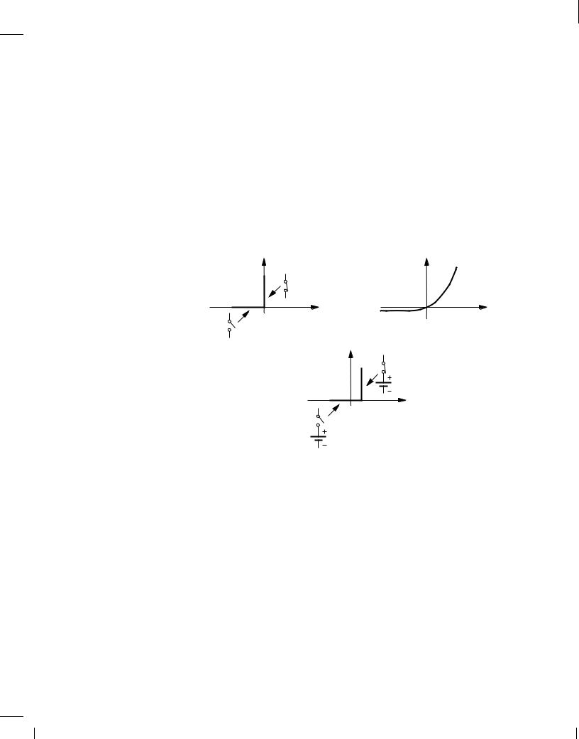
varies from ,1 to +1.
Solution
If VB is very negative, D1 is always on because Vin ,Vp. In this case, the output average is equal to VB [Fig. 3.12(a)]. For ,Vp < VB < 0, D1 turns off at some point in the negative half cycle and remains off in the positive half cycle, yielding an average greater than ,Vp but less than VB. For VB = 0, the average reaches ,Vp=( ). Finally, for VB Vp, no limiting occurs and the average is equal to zero. Figure 3.12(b) sketches this behavior.
|
VB < − Vp |
|
|
− Vp <VB |
Vin |
|
|
Vin |
|
|
|
t |
Vout |
t |
VB |
− Vp |
VB |
− Vp |
|
|
||||
Vout = VB |
|
|
|
|
|
|
|
|
|
|
VB = 0 |
|
VB |
+ Vp <VB |
Vin |
|
|
+ Vp |
|
|
|
|
||
VB |
Vout |
t |
|
t |
|
|
|||
|
− |
Vp |
Vout |
|
|
|
|
||
|
|
|
(a) |
|
|
|
Vout |
|
|
|
− Vp |
|
+ Vp |
|
|
|
|
− Vp |
VB |
|
|
|
π |
|
|
|
|
− Vp |
|
|
1 |
|
|
|
(b)
Figure 3.12 .
Exercise
Repeat the above example if the terminals of the diode are swapped.
Example 3.11
Is the circuit of Fig. 3.11(b) a rectifier?
Solution
Yes, indeed. The circuit passes only negative cycles to the output, producing a negative average.
Exercise
How should the circuit of Fig. 3.11(b) be modified to pass only positive cycles to the output.
BR |
Wiley/Razavi/Fundamentals of Microelectronics [Razavi.cls v. 2006] |
June 30, 2007 at 13:42 |
72 (1) |
|
|
|
|
72 |
Chap. 3 |
Diode Models and Circuits |
3.2 PN Junction as a Diode
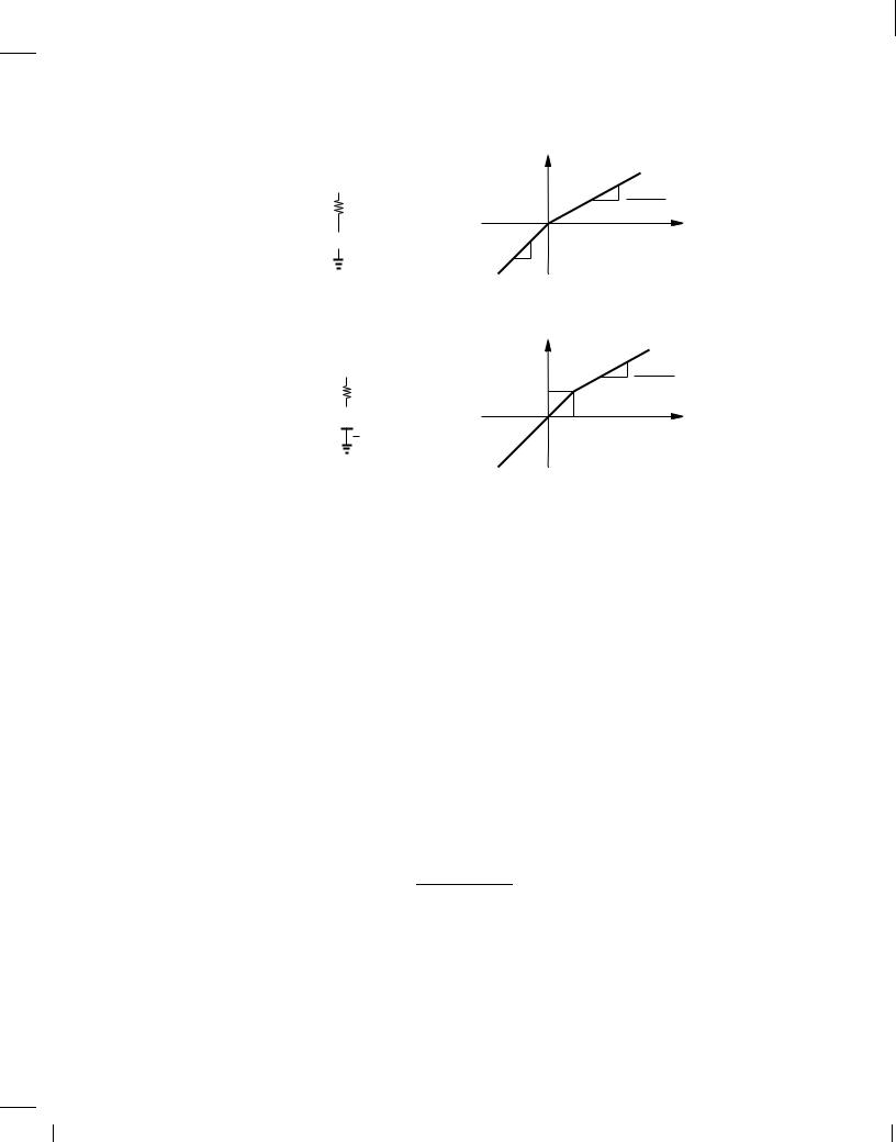
The operation of the ideal diode is somewhat reminiscent of the current conduction in pn junctions. In fact, the forward and reverse bias conditions depicted in Fig. 3.3(b) are quite similar to those studied for pn junctions in Chapter 2. Figures 3.13(a) and (b) plot the I/V characteristics of the ideal diode and the pn junction, respectively. The latter can serve as an approximation of the former by providing “unilateral” current conduction. Shown in Fig. 3.13 is the constant-voltage model developed in Chapter 2, providing a simple approximation of the exponential function and also resembling the characteristic plotted in Fig. 3.11(a).
I D |
I j |
VD |
|
Vj |
(a) |
|
(b) |
I D |
|
|
|
VD,on |
|
VD,on |
V |
D |
|
|
|
VD,on
(c)
Figure 3.13 Diode characteristics: (a) ideal model, (b) exponential model, (c) constant-voltage model.
Given a circuit topology, how do we choose one of the above models for the diodes? We may utilize the ideal model so as to develop a quick, rough understanding of the circuit's operation. Upon performing this exercise, we may discover that this idealization is inadequate and hence employ the constant-voltage model. This model suffices in most cases, but we may need to resort to the exponential model for some circuits. The following examples illustrate these points.
Example 3.12
Plot the input/output characteristic of the circuit shown in Fig. 3.14(a) using (a) the ideal model and (b) the constant-voltage model.
Solution
(a) We begin with Vin = ,1, recognizing that D1 is reverse biased. In fact, for Vin < 0, the diode remains off and no current flows through the circuit. Thus, the voltage drop across R1 is zero and Vout = Vin.
As Vin exceeds zero, D1 turns on, operating as a short and reducing the circuit to a voltage
BR |
Wiley/Razavi/Fundamentals of Microelectronics [Razavi.cls v. 2006] |
June 30, 2007 at 13:42 |
73 (1) |
|
|
|
|
Sec. 3.2 PN Junction as a Diode
R1 |
Vout |
Vin


 Vout
Vout
R2
D1 
1
(a) |
(b) |
Vout
R1
Vin


 Vout
Vout
|
|
R2 |
VD,on |
|
|
||
|
|
VD,on |
VD,on |
|
|
||
|
|
 1
1
(d)
(c)
73
R2
R2 |
+ R1 |
Vin
R2
R2 |
+ R1 |
Vin
Figure 3.14 (a) Diode circuit, (b) input/output characteristic with ideal diode model, (c) input/output characteristic with constant-voltage diode model .
divider. That is,
Vout = |
|
R2 |
Vin for Vin > 0: |
(3.9) |
R1 |
+ R2 |
Figure 3.14(b) plots the overall characteristic, revealing a slope equal to unity for Vin < 0 and R2=(R2 + R1) for Vin > 0. In other words, the circuit operates as a voltage divider once the diode turns on and loads the output node with R2.
(b) In this case, D1 is reverse biased for Vin < VD;on, yielding Vout = Vin. As Vin exceeds VD;on, D1 turns on, operating as a constant voltage source with a value VD;on [as illustrated in Fig. 3.13(c)]. Reducing the circuit to that in Fig. 3.14(c), we apply Kirchoff's current law to the output node:
Vin , Vout = Vout , VD;on : |
(3.10) |
||
R1 |
R2 |
|
|
It follows that |
|
|
|
|
R2 Vin + VD;on |
|
|
Vout = |
R1 |
: |
(3.11) |
1 + |
R2 |
|
|
|
|
R1 |
|
As expected, Vout = VD;on if Vin = VD;on. Figure 3.14(d) plots the resulting characteristic, displaying the same shape as that in Fig. 3.14(b) but with a shift in the break point.
Exercise
In the above example, plot the current through R1 as a function of Vin.
BR |
Wiley/Razavi/Fundamentals of Microelectronics [Razavi.cls v. 2006] |
June 30, 2007 at 13:42 |
74 (1) |
|
|
|
|
74 |
Chap. 3 |
Diode Models and Circuits |
3.3 Additional Examples
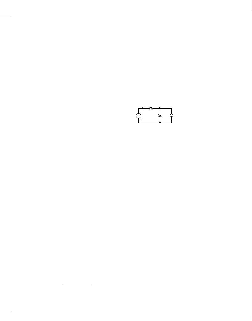
Example 3.13
In the circuit of Fig. 3.15, D1 and D2 have different cross section areas but are otherwise identical. Determine the current flowing through each diode.
I in |
R1 |
V1 |
D1 D2 |
Figure 3.15 Diode circuit.
Solution
In this case, we must resort to the exponential equation because the ideal and constant-voltage models do not include the device area. We have
Iin = ID1 + ID2: |
(3.12) |
||||
We also equate the voltages across D1 and D2: |
|
|
|
||
VT ln ID1 |
= VT ln |
ID2 ; |
(3.13) |
||
IS1 |
|
|
|
IS2 |
|
that is, |
|
|
|
|
|
ID1 |
= |
ID2 : |
|
(3.14) |
|
IS1 |
|
|
IS2 |
|
|
Solving (3.12) and (3.14) together yields |
|
|
|
|
|
ID1 = |
|
|
Iin |
|
(3.15) |
|
1 + IS2 |
|
|||
|
|
|
|
||
|
|
|
IS1 |
|
|
ID2 = |
|
|
Iin |
: |
(3.16) |
|
1 + IS1 |
||||
|
|
|
|
||
|
|
|
IS2 |
|
|
As expected, ID1 = ID2 = Iin=2 if IS1 = IS2.
Exercise
For the circuit of Fig. 3.15, calculate VD is terms of Iin; IS1; and IS2.
This section can be skipped in a first reading
BR |
Wiley/Razavi/Fundamentals of Microelectronics [Razavi.cls v. 2006] |
June 30, 2007 at 13:42 |
75 (1) |
|
|
|
|
Sec. 3.3 |
Additional Examples |
75 |
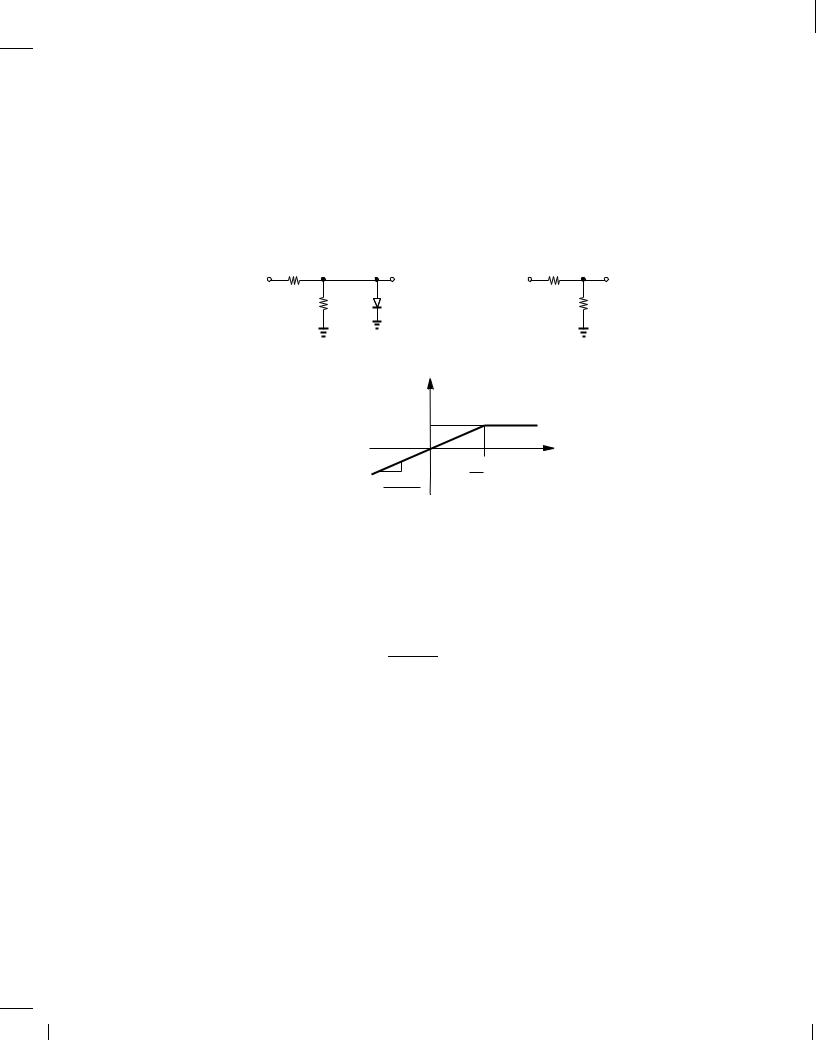
Example 3.14
Using the constant-voltage model plot the input/output characteristics of the circuit depicted in Fig. 3.16(a). Note that a diode about to turn on carries zero current but sustains VD;on.
R1 |
|
|
|
R1 |
Vin |
Vout |
|
Vin |
Vout |
R2 |
D1 |
|
|
R2 |
(a) |
|
|
|
(b) |
|
Vout |
|
|
|
|
VD,on |
|
|
|
|
(1 |
R1 |
) VD,on |
Vin |
|
+ |
|
||
|
R2 |
R2 |
|
|
|
R2 + R1 |
|
|
|
(c)
Figure 3.16 (a) Diode circuit, (b) equivalent circuit when D1 is off, (c) input/output characteristic.
Solution
In this case, the voltage across the diode happens to be equal to the output voltage. We note that if Vin = ,1, D1 is reverse biased and the circuit reduces to that in Fig. 3.16(b). Consequently,
R2 |
|
(3.17) |
vout = R1 + R2 |
Vin: |
At what point does D1 turn on? The diode voltage must reach VD;on, requiring an input voltage given by:
|
|
R2 |
|
(3.18) |
|
|
|
Vin = VD;on; |
|||
|
R1 + R2 |
||||
and hence |
|
|
|
|
|
V |
in |
= 1 + R1 |
V : |
(3.19) |
|
|
|
R2 |
D;on |
|
|
|
|
|
|
|
|
The reader may question the validity of this result: if the diode is indeed on, it draws current and the diode voltage is no longer equal to [R2=(R1 +R2)]Vin. So why did we express the diode voltage as such in Eq. (3.18)? To determine the break point, we assume Vin gradually increases so that it places the diode at the edge of the turn-on, e.g., it creates Vout 799 mV. The diode therefore still draws no current, but the voltage across it and hence the input voltage are almost sufficient to turn it on.
BR |
Wiley/Razavi/Fundamentals of Microelectronics [Razavi.cls v. 2006] |
June 30, 2007 at 13:42 |
76 (1) |
|
|
|
|
76 |
Chap. 3 |
Diode Models and Circuits |
For Vin > (1 + R1=R2)VD;on, D1 remains forward-biased, yielding Vout = VD;on. Figure 3.16(c) plots the overall characteristic.
Exercise
Repeat the above example but assume the terminals of D1 are swapped, i.e., the anode is tied to ground and the cathode the output node.
Exercise
For the above example, plot the current through R1 as a function of Vin.
Example 3.15
Plot the input/output characteristic for the circuit shown in Fig. 3.17(a). Assume a constantvoltage model for the diode.
|
D 1 |
R1 |
|
|
|
X |
|
||
Vin |
X |
Vout |
||
Vout |
||||
|
||||
|
R2 |
VD,on D1 R2 |
|
|
|
R1 |
|
||
|
|
Vin = − |
|
|
|
(a) |
(b) |
|
Vout 
R2
Vin |
Vout |
(1 + |
R1 |
)VD,on |
|
R1 |
R2 |
||
|
|
|
||
|
|
|
|
|
|
|
|
1 |
|
R1
R1 |
+ R2 |
Vin
(c) |
(d) |
Figure 3.17 (a) Diode circuit, (b) illustration for very negative inputs, (c) equivalent circuit when D1 is off, (d) input/output characteristic.
Solution
We begin with Vin = ,1, and redraw the circuit as depicted in Fig. 3.17(b), placing the more negative voltages on the bottom and the more positive voltages on the top. This diagram suggests that the diode operates in forward bias, establishing a voltage at node X equal to Vin + VD;on. Note that in this regime, VX is independent of R2 because D1 acts as a battery. Thus, so long as D1 is on, we have
Vout = Vin + VD;on: |
(3.20) |

BR |
Wiley/Razavi/Fundamentals of Microelectronics [Razavi.cls v. 2006] |
June 30, 2007 at 13:42 |
77 (1) |
|
|
|
|
Sec. 3.3 Additional Examples 77
We also compute the current flowing through R2 and R1: |
|
|
I |
= VD;on |
(3.21) |
R2 |
R2 |
|
|
|
|
I |
= 0 , VX |
(3.22) |
R1 |
R1 |
|
|
|
|
|
= ,(Vin + VD;on): |
(3.23) |
|
R1 |
|
Thus, as Vin increases from ,1, IR2 remains constant but jIR1j decreases; i.e., at some point
IR2 = IR1.
At what point does D1 turn off? Interestingly, in this case it is simpler to seek the condition that results in a zero current through the diode rather than insufficient voltage across it. The observation that at some point, IR2 = IR1 proves useful here as this condition also implies that D1 carries no current (KCL at node X). In other words, D1 turns off if Vin is chosen to yield IR2 = IR1. From (3.21) and (3.23),
VD;on = ,Vin + VD;on |
(3.24) |
||||||
R2 |
|
|
R1 |
|
|
|
|
and hence |
|
|
|
|
|
|
|
V = ,(1 + |
R1 )V |
D;on |
: |
(3.25) |
|||
in |
|
|
R2 |
|
|
|
|
|
|
|
|
|
|
|
|
As Vin exceeds this value, the circuit reduces to that shown in Fig. 3.17(c) and |
|
||||||
Vout |
= |
R1 |
Vin: |
|
(3.26) |
||
R1 |
+ R2 |
|
|||||
The overall characteristic is shown in Fig. 3.17(d).
The reader may find it interesting to recognize that the circuits of Figs. 3.16(a) and 3.17(a) are identical: in the former, the output is sensed across the diode whereas in the latter it is sensed across the series resistor.
Exercise
Repeat the above example if the terminals of the diode are swapped.
As mentioned in Example 3.4, in more complex circuits, it may be difficult to correctly predict the region of operation of each diode by inspection. In such cases, we may simply make a guess, proceed with the analysis, and eventually determine if the final result agrees or conflicts with the original guess. Of course, we still apply intuition to minimize the guesswork. The following example illustrates this approach.
Example 3.16
Plot the input/output characteristic of the circuit shown in Fig. 3.18(a) using the constant-voltage diode model.
Solution
We begin with Vin = ,1, predicting intuitively that D1 is on. We also (blindly) assume that D2
BR |
Wiley/Razavi/Fundamentals of Microelectronics [Razavi.cls v. 2006] |
June 30, 2007 at 13:42 |
78 (1) |
|
|
|
|
78 |
|
|
|
|
|
|
|
|
|
Chap. 3 |
|
Diode Models and Circuits |
||
|
|
|
|
|
I R2 = |
|
R2 |
|
|
|
|
|
R2 |
|
|
|
|
|
|
|
|
|
|
Vout |
|
|
|
||
D 1 |
X R1 |
|
|
|
|
|
|
|
|
|
|
Vout |
||
|
|
|
I R1 R |
|
|
|
VB |
|
|
|
|
|||
Vin |
|
|
|
|
1 |
|
|
|
R |
1 |
|
VB |
||
|
|
|
|
Vout |
|
|
|
|
|
|||||
|
|
|
|
X |
|
Y |
I 1 |
= |
|
|
|
|||
|
|
|
|
|
|
X |
|
Y |
||||||
|
Y |
|
|
R1 |
|
|
|
|
|
|
||||
D 2 |
|
|
VD,on |
|
|
|
VD,on |
|
VD,on |
|
|
|
||
|
VB= 2 V |
|
|
|
|
|
|
|
|
|
|
|
||
|
|
|
|
|
|
Vin |
= − |
|
|
|
|
Vin |
= − |
|
|
|
|
|
|
|
|
|
|
|
|
|
|||
|
(a) |
|
|
|
|
|
(b) |
|
|
|
|
|
(c) |
|
|
D 1 |
X |
R |
1 |
|
|
|
|
|
D 1 |
X |
R |
1 |
|
|
|
|
|
|
|
|
|
|
|
|
||||
Vin |
|
|
|
|
Vout |
|
Vin = − VD,on |
|
|
|
Vout |
|||
|
D 2 Y |
VB |
R1 |
|
|
|
|
D 2 |
Y |
|
|
R1 |
||
|
|
|
|
|
|
|
|
|
VB= 2 V |
|||||
|
(d) |
|
|
|
|
|
|
|
|
(e) |
|
|
|
|
Vout |
|
|
|
|
|
|
|
|
|
|
|
|
|
Vout |
− VD,on |
|
|
|
|
D 1 |
X |
R |
1 |
|
|
|
|
− |
VD,on |
|
|
|
|
|
|
|
|
|
|
|||||
|
|
|
|
Vin |
|
|
|
|
Vout |
|
|
|||
|
|
|
Vin |
|
|
|
|
|
|
|
Vin |
|||
|
|
|
|
Y |
|
|
|
R1 |
|
|
|
|||
|
|
|
|
|
D 2 |
VB= 2 V |
|
|
|
|
||||
D 1 turns off. |
|
|
|
|
|
|
|
|
|
|
|
|||
|
|
|
|
|
|
|
|
|
|
|
|
|
|
|
(f) |
|
|
|
|
|
(g) |
|
|
|
|
|
|
|
(h) |
Figure 3.18 (a) Diode circuit, (b) possible equivalent circuit for very negative inputs, (c) simplified circuit,
(d) equivalent circuit, (e) equivalent circuit for Vin = ,VD;on, (f) section of input/output characteristic,
(g) equivalent circuit, (f) complete input/output characteristic.
is on, thus reducing the circuit to that in Fig. 3.18(b). The path through VD;on and VB creates a difference of VD;on + VB between Vin and Vout, i.e., Vout = Vin , (VD;on + VB). This voltage difference also appears across the branch consisting of R1 and VD;on, yielding
R1IR1 + VD;on = ,(VB + VD;on); |
(3.27) |
|
and hence |
|
|
IR1 |
= ,VB , 2VD;on : |
(3.28) |
|
R1 |
|
That is, IR1 is independent of Vin. We must now analyze these results to determine whether they agree with our assumptions regarding the state of D1 and D2. Consider the current flowing through R2:
IR2 |
= ,Vout |
(3.29) |
|
R2 |
|

BR |
Wiley/Razavi/Fundamentals of Microelectronics [Razavi.cls v. 2006] |
June 30, 2007 at 13:42 |
79 (1) |
|
|
|
|
Sec. 3.4 |
Large-Signal and Small-Signal Operation |
79 |
|
|
= ,Vin , |
(VD;on , VB); |
(3.30) |
|
|
R2 |
|
which approaches +1 for Vin = ,1. The large value of IR2 and the constant value of IR1 indicate that the branch consisting of VB and D2 carries a large current with the direction shown. That is, D2 must conduct current from its cathode to it anode, which is not possible.
In summary, we have observed that the forward bias assumption for D2 translates to a current in a prohibited direction. Thus, D2 operates in reverse bias for Vin = ,1. Redrawing the circuit as in Fig. 3.18(c) and noting that VX = Vin + VD;on, we have
Vout = (Vin + VD;on) |
|
R2 |
: |
(3.31) |
R1 |
+ R2 |
We now raise Vin and determine the first break point, i.e., the point at which D1 turns off or D2 turns on. Which one occurs first? Let us assume D1 turns off first and obtain the corresponding value of Vin. Since D2 is assumed off, we draw the circuit as shown in Fig. 3.18(d). Assuming that D1 is still slightly on, we recognize that at Vin ,VD;on, VX = Vin + VD;on approaches zero, yielding a zero current through R1, R2, and hence D1. The diode therefore turns off at
Vin = ,VD;on.
We must now verify the assumption that D2 remains off. Since at this break point, VX = Vout = 0, the voltage at node Y is equal to +VB whereas the cathode of D2 is at ,VD;on [Fig. 3.18(e)]. In other words, D2 is indeed off. Fig. 3.18(f) plots the input-output characteristic to the extent computed thus far, revealing that Vout = 0 after the first break point because the current flowing through R1 and R2 is equal to zero.
At what point does D2 turn on? The input voltage must exceed VY by VD;on. Before D2 turns on, Vout = 0, and VY = VB; i.e., Vin must reach VB + VD;on, after which the circuit is configured as shown in Fig. 3.18(g). Consequently,
Vout = Vin , VD;on , VB: |
(3.32) |
Figure 3.18(h) plots the overall result, summarizing the regions of operation.
Exercise
In the above example, assume D2 turns on before D1 turns off and show that the results conflict with the assumption.
3.4 Large-Signal and Small-Signal Operation
Our treatment of diodes thus far has allowed arbitrarily large voltage and current changes, thereby requiring a “general” model such as the exponential I/V characteristic. We call this regime “largesignal operation” and the exponential characteristic the “large-signal model” to emphasize that the model can accommodate arbitrary signal levels. However, as seen in previous examples, this model often complicates the analysis, making it difficult to develop an intuitive understanding of the circuit's operation. Furthermore, as the number of nonlinear devices in the circuit increases, “manual” analysis eventually becomes impractical.
The ideal and constant-voltage diode models resolve the issues to some extent, but the sharp nonlinearity at the turn-on point still proves problematic. The following example illustrates the general difficulty.
BR |
Wiley/Razavi/Fundamentals of Microelectronics [Razavi.cls v. 2006] |
June 30, 2007 at 13:42 |
80 (1) |
|
|
|
|
80 |
Chap. 3 |
Diode Models and Circuits |
Example 3.17
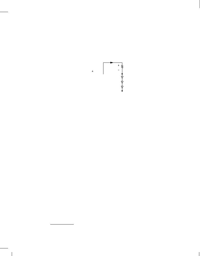
Having lost his 2.4-V cellphone charger, an electrical engineering student tries several stores but does not find adaptors with outputs less than 3 V. He then decides to put his knowledge of electronics to work and constructs the circuit shown in Fig. 3.19, where three identical diodes in forward bias produce a total voltage of Vout = 3VD 2:4 V and resistor R1 sustains the remaining 600 mV. Neglect the current drawn by the cellphone.6 (a) Determine the reverse
I X
600 mV R1 = 100 Ω
Vad = 3 V |
Adaptor |
|
|
|
|
|
|
|
|
|
|
|||
|
|
|
Vout |
|
|
|||||||||
|
|
|
|
|||||||||||
|
|
|
|
|
|
|
|
Cellphone |
||||||
|
|
|
|
|
|
|
|
|||||||
|
|
|
|
|
|
|
|
|
|
|
|
|
||
|
|
|
|
|
|
|
|
|
|
|
|
|
||
|
|
|
|
|
|
|
|
|
|
|
|
|
|
|
|
|
|
|
|
|
|
|
|
|
|
|
|
|
|
Figure 3.19 Adaptor feeding a cellphone.
saturation current, IS1 so that Vout = 2:4 V. (b) Compute Vout if the adaptor voltage is in fact 3.1 V.
Solution
(a) With Vout = 2:4 V, the current flowing through R1 is equal to |
|
|||
IX |
= Vad , Vout |
(3.33) |
||
|
|
|
R1 |
|
|
= 6 mA: |
(3.34) |
||
We note that each diode carries IX and hence |
|
|
|
|
I |
= I |
S |
exp VD : |
(3.35) |
X |
|
VT |
|
|
|
|
|
|
|
It follows that |
|
|
|
|
6 mA = I exp 800 mV |
(3.36) |
|||
|
S |
26 mV |
|
|
|
|
|
|
|
and |
|
|
|
|
IS = 2:602 10,16 A: |
(3.37) |
|||
(b) If Vad increases to 3.1 V, we expect that Vout increases only slightly. To understand why, first suppose Vout remains constant and equal to 2.4 V. Then, the additional 0.1 V must drop across R1, raising IX to 7 mA. Since the voltage across each diode has a logarithmic dependence upon the current, the change from 6 mA to 7 mA indeed yields a small change in Vout.7
To examine the circuit quantitatively, we begin with IX = 7 mA and iterate:
Vout = 3VD |
(3.38) |
6Made for the sake of simplicity here, this assumption may not be valid.
7Recall from Eq. (2.109) that a tenfold change in a diode's current translates to a 60-mV change in its voltage.