

Fundamentals of Microelectronics
.pdfBR |
Wiley/Razavi/Fundamentals of Microelectronics [Razavi.cls v. 2006] |
June 30, 2007 at 13:42 |
91 (1) |
|
|
|
|
Sec. 3.5 |
Applications of Diodes |
91 |
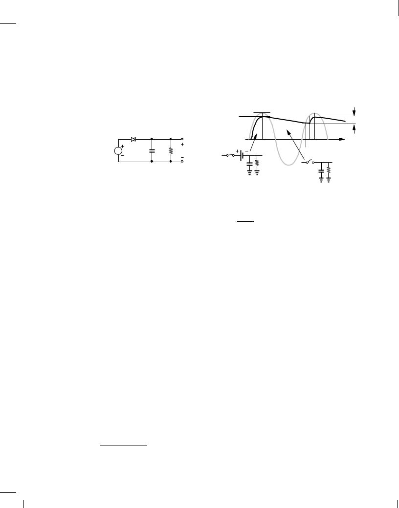
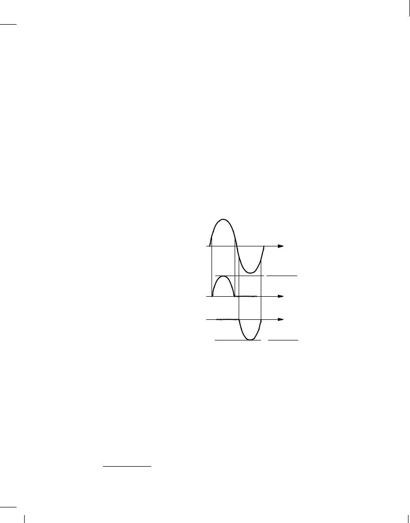
As suggested by the above example, the load can be represented by a simple resistor in some cases [Fig. 3.32(a)]. We must therefore repeat our analysis with RL present. From the waveforms in Fig. 3.32(b), we recognize that Vout behaves as before until t = t1, still exhibiting a value of Vin , VD;on = Vp , VD;on if the diode voltage is assumed relatively constant. However, as Vin begins to fall after t = t1, so does Vout because RL provides a discharge path for C1. Of course, since changes in Vout are undesirable, C1 must be so large that the current drawn by RL does not reduce Vout significantly. With such a choice of C1, Vout falls slowly and D1 remains reverse
biased.
Vp
|
|
Vp − VD,on |
Vout |
VR |
|
|
Vin |
|
|
|
|
|
|
|
|
D 1 |
|
|
|
|
|
t 1 |
t 3 |
t |
Vin |
C1 |
R L Vout |
t 2 |
|
(a) |
(b) |
Figure 3.32 (a) Rectifier driving a resistive load, (b) input and output waveforms.
The output voltage continues to decrease while Vin goes through a negative excursion and returns to positive values. At some point, t = t2, Vin and Vout become equal and slightly later, at t = t3, Vin exceeds Vout by VD;on, thereby turning D1 on and forcing Vout = Vin , VD;on. Hereafter, the circuit behaves as in the first cycle. The resulting variation in Vout is called the “ripple.” Also, C1 is called the “smoothing” or “filter” capacitor.
Example 3.26 
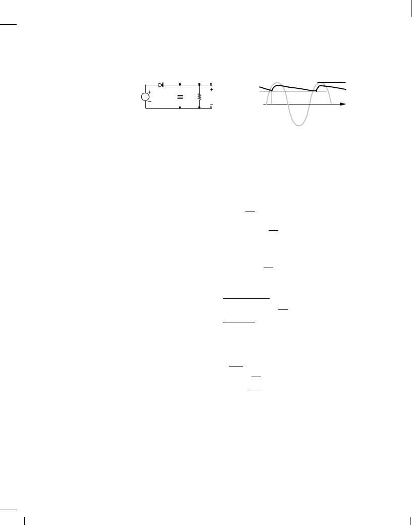
Sketch the output waveform of Fig. 3.32 as C1 varies from very large values to very small values.
Solution
If C1 is very large, the current drawn by RL when D1 is off creates only a small change in Vout. Conversely, if C1 is very small, the circuit approaches that in Fig. 3.28, exhibiting large variations in Vout. Figure 3.33 illustrates several cases.
Vin |
Large C1 |
|
|
|
Small C1 |
|
Vout |
t
Very Small C1
Figure 3.33 Output waveform of rectifier for different values of smoothing capacitor.
Exercise
Repeat the above example for different values of RL with C1 constant.
BR |
Wiley/Razavi/Fundamentals of Microelectronics [Razavi.cls v. 2006] |
June 30, 2007 at 13:42 |
92 (1) |
|
|
|
|
92 |
Chap. 3 |
Diode Models and Circuits |
Ripple Amplitude In typical applications, the (peak-to-peak) amplitude of the ripple, VR, in Fig. 3.32(b) must remain below 5 to 10% of the input peak voltage. If the maximum current drawn by the load is known, the value of C1 is chosen large enough to yield an acceptable ripple. To this end, we must compute VR analytically (Fig. 3.34). Since Vout = Vp , VD;on at t = t1, the discharge of C1 through RL can be expressed as:
|
|
Vp |
Vout |
|
|
|
Vp − VD,on |
VR |
|
|
|
Vin |
|
|
|
D 1 |
|
|
|
|
|
|
|
|
|
|
t 1 |
t 3 t 4 |
t |
Vin |
C1 |
R L Vout |
t 2 |
|
(a) |
(b) |
Figure 3.34 Ripple at output of a rectifier.
V |
out |
(t) = (V , V |
D;on |
) exp |
,t |
0 t t |
; |
(3.75) |
|
p |
|
RLC1 |
3 |
|
|
||
|
|
|
|
|
|
|
|
where we have chosen t1 = 0 for simplicity. To ensure a small ripple, RLC1 must be much greater than t3 , t1; thus, noting that exp(, ) 1 , for 1,
V |
|
(t) (V |
|
, V |
|
) 1 , |
t |
|
|
|
|
(3.76) |
|
out |
p |
D;on |
RLC1 |
|
|
|
|||||||
|
|
|
|
|
|
|
|
|
|
||||
|
|
|
|
|
|
|
|
|
|
|
|
|
|
|
|
(V |
|
, V |
|
) , Vp |
, VD;on |
|
t |
: |
(3.77) |
||
|
|
p |
D;on |
|
|||||||||
|
|
|
|
|
|
RL |
|
|
C1 |
|
|||
|
|
|
|
|
|
|
|
|
|
|
|||
The first term on the right hand side represents the initial condition across C1 and the second term, a falling ramp—as if a constant current equal to (Vp , VD;on)=RL discharges C1.15 This result should not come as a surprise because the nearly constant voltage across RL results in a relatively constant current equal to (Vp , VD;on)=RL.
The peak-to-peak amplitude of the ripple is equal to the amount of discharge at t = t3. Since t4 , t3 is equal to the input period, Tin, we write t3 , t1 = Tin , T , where T (= t4 , t3) denotes the time during which D1 is on. Thus,
VR = |
Vp , VD;on Tin , T : |
(3.78) |
|
|
RL |
C1 |
|
Recognizing that if C1 discharges by a small amount, then the diode turns on for only a brief period, we can assume T Tin and hence
VR |
Vp , VD;on |
Tin |
(3.79) |
|
RL |
C1 |
|
|
Vp , VD;on ; |
|
(3.80) |
|
RLC1fin |
|
|
This section can be skipped in a first reading.
15Recall that I = CdV=dt and hence dV = (I=C)dt.

BR |
Wiley/Razavi/Fundamentals of Microelectronics [Razavi.cls v. 2006] |
June 30, 2007 at 13:42 |
93 (1) |
|
|
|
|
Sec. 3.5 |
Applications of Diodes |
93 |
where fin = T ,1.
in
Example 3.27
A transformer converts the 110-V, 60-Hz line voltage to a peak-to-peak swing of 9 V. A halfwave rectifier follows the transformer to supply the power to the laptop computer of Example 3.25. Determine the minimum value of the filter capacitor that maintains the ripple below 0.1 V. Assume VD;on = 0:8 V.
Solution
We have Vp = 4:5 V, RL = 0:436 , and Tin = 16:7 ms. Thus,
C1 = |
Vp , VD;on |
Tin |
(3.81) |
|
VR |
RL |
|
= |
1:417 F: |
|
(3.82) |
This is a very large value. The designer must trade the ripple amplitude with the size, weight, and cost of the capacitor. In fact, limitations on size, weight, and cost of the adaptor may dictate a much greater ripple, e.g., 0.5 V, thereby demanding that the circuit following the rectifier tolerate such a large, periodic variation.
Exercise
Repeat the above example for 220-V, 50-Hz line voltage, assuming the transformer still produces a peak-to-peak swing of 9 V. Which mains frequency gives a more desirable choice of
C1?
In many cases, the current drawn by the load is known. Repeating the above analysis with the load represented by a constant current source or simply viewing (Vp , VD;on)=RL in Eq. (3.80) as the load current, IL, we can write
V = |
IL |
: |
(3.83) |
|
|||
R |
C1fin |
|
|
|
|
|
Diode Peak Current We noted in Fig. 3.30(b) that the diode must exhibit a reverse breakdown voltage of at least 2 Vp. Another important parameter of the diode is the maximum forward bias current that it must tolerate. For a given junction doping profile and geometry, if the current exceeds a certain limit, the power dissipated in the diode (= VDID) may raise the junction temperature so much as to damage the device.
We recognize from Fig. 3.35, that the diode current in forward bias consists of two components: (1) the transient current drawn by C1, C1dVout=dt, and (2) the current supplied to RL, approximately equal to (Vp ,VD;on)=RL. The peak diode current therefore occurs when the first component reaches a maximum, i.e., at the point D1 turns on because the slope of the output waveform is maximum. Assuming VD;on Vp for simplicity, we note that the point at which D1 turns on is given by Vin(t1) = Vp , VR. Thus, for Vin(t) = Vp sin !int,
Vp sin !int1 = Vp , VR; |
(3.84) |
This section can be skipped in a first reading.
BR |
Wiley/Razavi/Fundamentals of Microelectronics [Razavi.cls v. 2006] |
June 30, 2007 at 13:42 |
94 (1) |
|
|
|
|
94 |
|
|
Chap. 3 |
Diode Models and Circuits |
|
|
D 1 |
|
Vin |
Vout |
Vp |
|
|
|
|
||
Vin |
C1 |
R L |
Vp− VR |
|
|
Vout |
|
|
|||
|
|
|
t 1 |
|
t |
Figure 3.35 Rectifier circuit for calculation of ID.
and hence
sin!int1 = 1 , VR : Vp
With VD;on neglected, we also have Vout(t) Vin (t), obtaining the diode current as
ID1(t) = C1 dVout + Vp dt RL
= C1!inVp cos !int + Vp : RL
This current reaches a peak at t = t1:
Ip = C1!inVp cos !int1 + Vp ;
RL
which, from (3.85), reduces to
Ip = C1!inVps1 , 1 , VR 2 + Vp
Vp RL
|
|
|
2VR |
|
V 2 |
Vp |
|
= C ! |
in |
V s |
|
, |
R + |
|
: |
|
|
||||||
1 |
p |
Vp |
|
Vp2 |
RL |
|
|
|
|
|
|
|
Since VR Vp, we neglect the second term under the square root:
Ip C1!inVps2VR + Vp
Vp RL
|
Vp |
R C ! s2VR |
+ 1!: |
|
|
||||
|
RL |
L 1 in |
Vp |
|
|
|
|
||
(3.85)
(3.86)
(3.87)
(3.88)
(3.89)
(3.90)
(3.91)
(3.92)
Example 3.28
Determine the peak diode current in Example 3.27 assuming VD;on 0 and C1 = 1:417 F.
Solution
We have Vp = 4:5 V, RL = 0:436 , !in = 2 (60 Hz), and VR = 0:1 V. Thus, |
|
Ip = 517 A: |
(3.93) |
BR |
Wiley/Razavi/Fundamentals of Microelectronics [Razavi.cls v. 2006] |
June 30, 2007 at 13:42 |
95 (1) |
|
|
|
|
Sec. 3.5 |
Applications of Diodes |
95 |
This value is extremely large. Note that the current drawn by C1 is much greater than that flowing through RL.
Exercise
Repeat the above example if C1 = 1000 F.
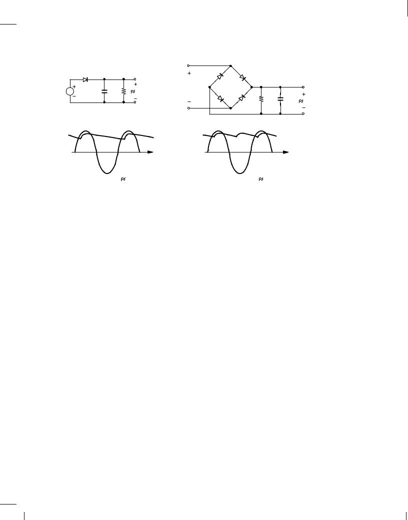
Full-Wave Rectifier The half-wave rectifier studied above blocks the negative half cycles of the input, allowing the filter capacitor to be discharged by the load for almost the entire period. The circuit therefore suffers from a large ripple in the presence of a heavy load (a high current).
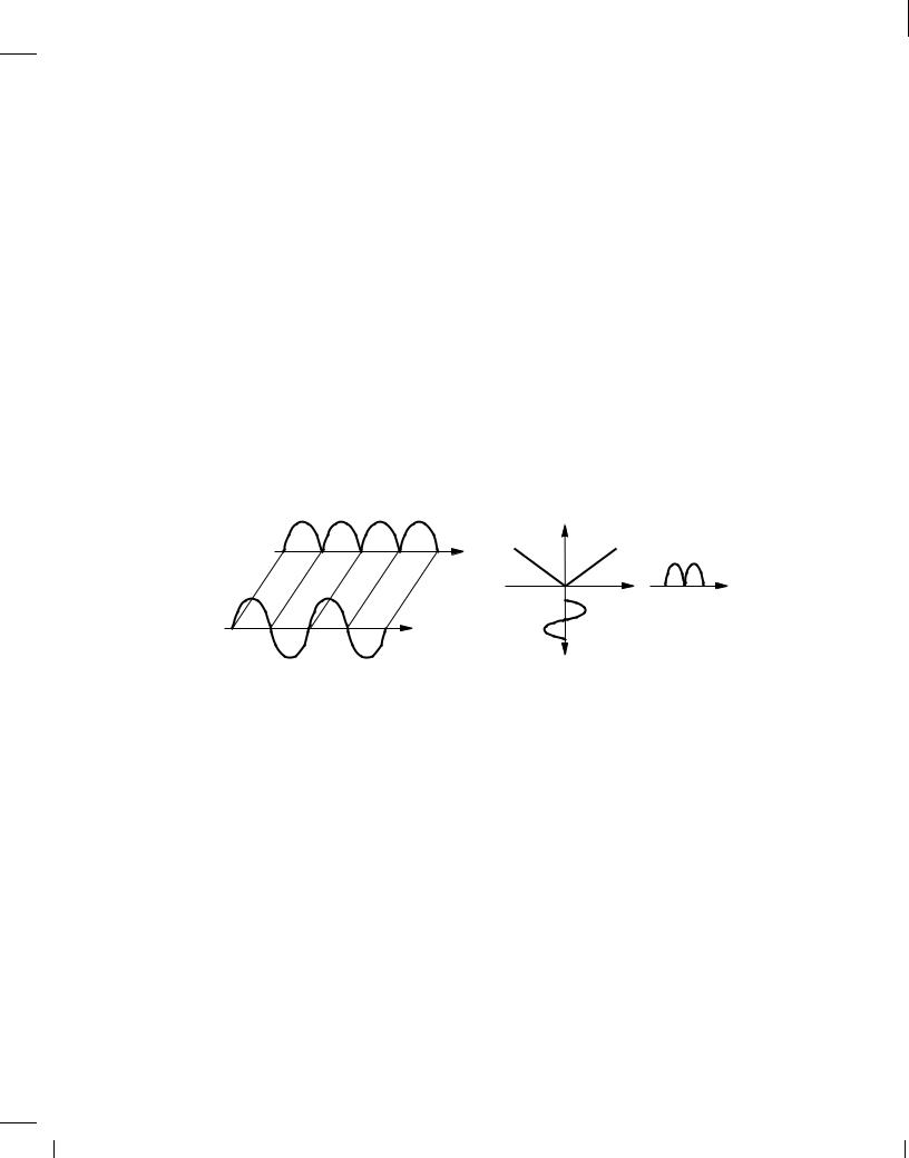
It is possible to reduce the ripple voltage by a factor of two through a simple modification. Illustrated in Fig. 3.36(a), the idea is to pass both positive and negative half cycles to the output, but with the negative half cycles inverted (i.e., multiplied by ,1). We first implement a circuit that performs this function [called a “full-wave rectifier” (FWR)] and next prove that it indeed exhibits a smaller ripple. We begin with the assumption that the diodes are ideal to simplify the task of circuit synthesis. Figure 3.36(b) depicts the desired input/output characteristic of the full-wave rectifier.
y (t ) |
Vout |
|
|
|
|
t |
|
Vout |
x (t ) |
Vin |
t |
|
|
|
t |
t |
|
|
|
|
(a) |
(b) |
|
Figure 3.36 (a) Input and output waveforms and (b) input/output characteristic of a full-wave rectifier.
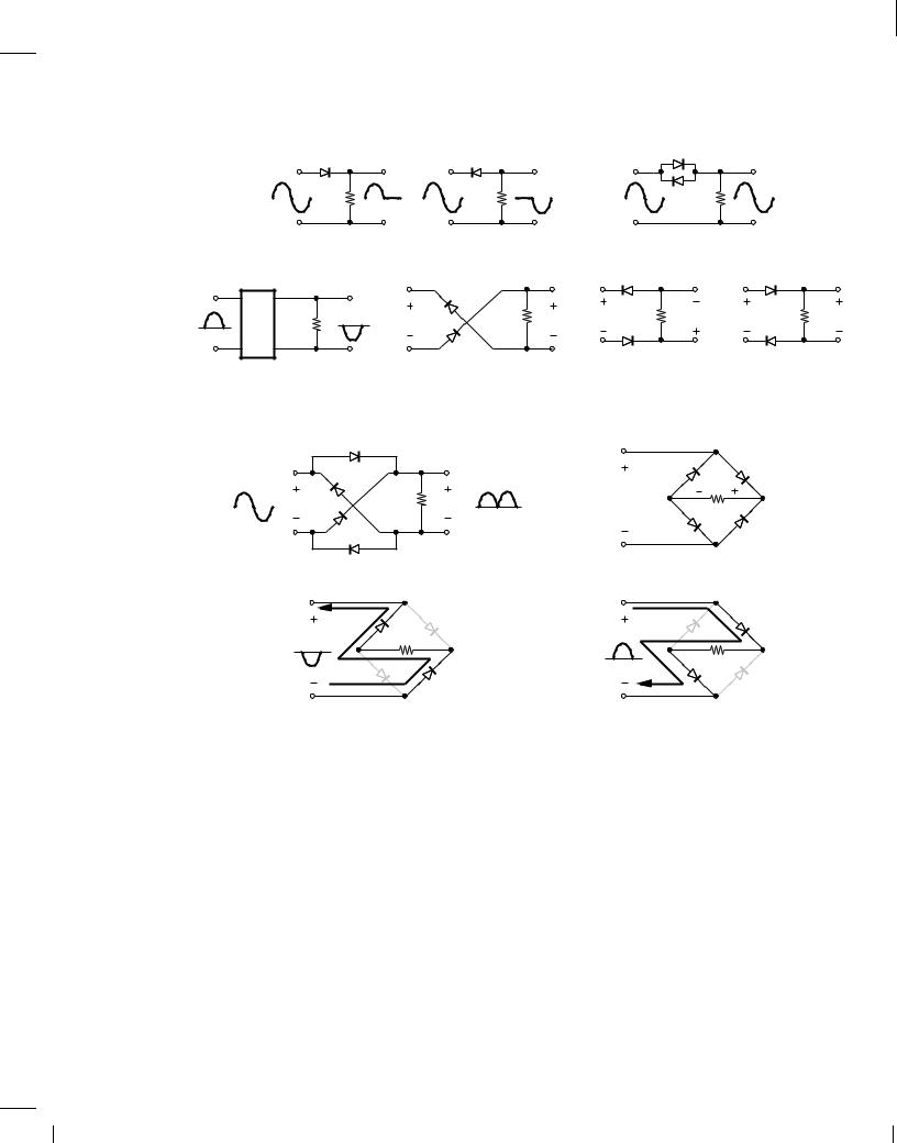
Consider the two half-wave rectifiers shown in Fig. 3.37(a), where one blocks negative half cycles and the other, positive half cycles. Can we combine these circuits to realize a full-wave rectifier? We may attempt the circuit in Fig. 3.37(b), but, unfortunately, the output contains both positive and negative half cycles, i.e., no rectification is performed because the negative half cycles are not inverted. Thus, the problem is reduced to that illustrated in Fig. 3.37(c): we must first design a half-wave rectifier that inverts. Shown in Fig. 3.37(d) is such a topology, which can also be redrawn as in Fig. 3.37(e) for simplicity. Note the polarity of Vout in the two diagrams. Here, if Vin < 0, both D2 and D1 are on and Vout = ,Vin. Conversely, if Vin > 0, both diodes are off, yielding a zero current through RL and hence Vout = 0. In analogy with this circuit, we also compose that in Fig. 3.37(f), which simply blocks the negative input half cycles; i.e.,
Vout = 0 for Vin < 0 and Vout = Vin for Vin > 0.
With the foregoing developments, we can now combine the topologies of Figs. 3.37(d) and (f) to form a full-wave rectifier. Depicted in Fig. 3.38(a), the resulting circuit passes the negative half cycles through D1 and D2 with a sign reversal [as in Fig. 3.37(d)] and the positive half cycles through D3 and D4 with no sign reversal [as in Fig. 3.37(f)]. This configuration is usually drawn as in Fig. 3.38(b) and called a “bridge rectifier.”
Let us summarize our thoughts with the aid of the circuit shown in Fig. 3.38(b). If Vin < 0, D2 and D1 are on and D3 and D4 are off, reducing the circuit to that shown in Fig. 3.38(c) and
BR |
Wiley/Razavi/Fundamentals of Microelectronics [Razavi.cls v. 2006] |
June 30, 2007 at 13:42 |
96 (1) |
|
|
|
|
96 |
|
|
|
|
Chap. 3 |
Diode Models and Circuits |
|
|
||||
|
D 1 |
|
D 2 |
|
|
|
|
|
|
|
|
|
|
R L |
|
R L |
|
|
|
|
R L |
|
|
|
|
|
|
(a) |
|
|
|
|
|
(b) |
|
|
|
|
|
|
|
|
|
|
D 2 |
|
|
|
D 3 |
|
|
|
|
|
D 2 |
|
|
|
|
|
|
|
|
|
? |
R L |
Vin |
R |
|
Vin |
R |
|
Vout |
Vin |
R |
|
Vout |
|
L |
Vout |
|
L |
|
|
|
L |
|
|||
|
|
|
D 1 |
|
|
D 1 |
|
|
|
D 4 |
|
|
|
|
|
|
|
|
|
|
|
|
|
||
|
(c) |
|
(d) |
|
|
|
(e) |
|
|
(f) |
|
|
Figure 3.37 (a) Rectification of each half cycle, (b) no rectification, (c) rectification and inversion, (d) |
|
|
||||||||||
realization of (c), (e) path for negative half cycles, (f) path for positive half cycles. |
|
|
|
|
|
|||||||
|
|
|
|
|
|
|
|
D 2 |
D 3 |
|
|
|
|
|
|
|
|
|
Vin |
|
Vout |
|
|
|
|
|
V |
R L |
V |
|
|
|
|
|
|
|
|
|
|
in |
|
out |
|
|
|
|
RL |
|
|
|
|
|
|
|
|
|
|
|
|
D 1 |
|
|
|
|
|
|
|
|
|
|
|
|
D 4 |
|
|
|
|
|
|
(a) |
|
|
|
|
|
(b) |
|
|
|
|
|
|
D 2 |
D 3 |
|
|
|
|
D 2 |
D 3 |
|
|
|
|
Vin |
|
|
|
Vin |
|
|
|
|
|
|
|
|
|
D 4 |
D 1 |
|
|
|
|
D 4 |
D 1 |
|
|
|
|
|
|
|
|
|
|
|
|
|
|||
|
|
(c) |
|
|
|
|
|
(d) |
|
|
|
|
Figure 3.38 (a) Full-wave rectifier, (b) simplified diagram, (c) current path for negative input, (d) current |
|
|
||||||||||
path for positive input. |
|
|
|
|
|
|
|
|
|
|
|
|
yielding Vout = ,Vin. On the other hand, if Vin > 0, the bridge is simplified as shown in Fig. 3.38(d), and Vout = Vin.
How do these results change if the diodes are not ideal? Figures 3.38(c) and (d) reveal that the circuit introduces two forward-biased diodes in series with RL, yielding Vout = ,Vin , 2VD;on for Vin < 0. By contrast, the half-wave rectifier in Fig. 3.28 produces Vout = Vin , VD;on. The drop of 2VD;on may pose difficulty if Vp is relatively small and the output voltage must be close to Vp.
Example 3.29
Assuming a constant-voltage model for the diodes, plot the input/output characteristic of a full-wave rectifier.
Solution
The output remains equal to zero for jVinj < 2VD;on and “tracks” the input for jVinj > VD;on
BR |
Wiley/Razavi/Fundamentals of Microelectronics [Razavi.cls v. 2006] |
June 30, 2007 at 13:42 |
97 (1) |
|
|
|
|
Sec. 3.5 |
Applications of Diodes |
97 |
with a slope of unity. Figure 3.39 plots the result.
Vout 
Vout |
|
Vin |
t |
−2 VD,on +2V D,on |
|
t 
Figure 3.39 Input/output characteristic of full-wave rectifier with nonideal diodes.
Exercise
What is the slope of the characteristic for jVinj > 2VD;on?
We now redraw the bridge once more and add the smoothing capacitor to arrive at the complete design [Fig. 3.40(a)]. Since the capacitor discharge occurs for about half of the input cycle, the ripple is approximately equal to half of that in Eq. (3.80):
D 2 |
D 3 |
|
|
Vin |
||
|
|
|
||||
Vin |
|
|
|
|
|
t |
D |
4 |
D |
1 |
RL |
C1 |
V |
|
|
|
|
out |
||
Vout
|
|
|
(a) |
|
|
|
|
|
|
|
A |
|
|
|
|
|
D 2 |
D 3 |
|
|
|
||
V |
B |
|
VD,on |
|
|
|
|
in |
|
|
|
|
|
|
|
|
D |
4 |
D |
1 |
RL |
C1 |
V |
|
|
|
|
|
out |
||
(b)
Figure 3.40 (a) Ripple in full-wave rectifier, (b) equivalent circuit.
VR 1 Vp , 2VD;on ;
2 RLC1fin
where the numerator reflects the drop of 2VD;on due to the bridge.
t
(3.94)
BR |
Wiley/Razavi/Fundamentals of Microelectronics [Razavi.cls v. 2006] |
June 30, 2007 at 13:42 |
98 (1) |
|
|
|
|
98 |
Chap. 3 |
Diode Models and Circuits |
In addition to a lower ripple, the full-wave rectifier offers another important advantage: the maximum reverse bias voltage across each diode is approximately equal to Vp rather than 2Vp. As illustrated in Fig. 3.40(b), when Vin is near Vp and D3 is on, the voltage across D2, VAB, is simply equal to VD;on + Vout = Vp , VD;on. A similar argument applies to the other diodes.
Another point of contrast between half-wave and full-wave rectifiers is that the former has a common terminal between the input and output ports (node G in Fig. 3.28), whereas the latter does not. In Problem 38, we study the effect of shorting the input and output grounds of a fullwave rectifier and conclude that it disrupts the operation of the circuit.
Example 3.30
Plot the currents carried by each diode in a bridge rectifier as a function of time for a sinusoidal input. Assume no smoothing capacitor is connected to the output.
Solution
From Figs. 3.38(c) and (d), we have Vout = ,Vin + 2VD;on for Vin < ,2VD;on and Vout = Vin , 2VD;on for Vin > +2VD;on. In each half cycle, two of the diodes carry a current equal to Vout=RL and the other two remain off. Thus, the diode currents appear as shown in Fig. 3.41.
Vin
|
t |
|
Vp − 2 VD,on |
I D1 = I D2 |
R L |
t
I D3 = I D4
t
Vp − 2 VD,on
−
R L
Figure 3.41 Currents carried by diodes in a full-wave rectifier.
Exercise
Sketch the power consumed in each diode as a function of time.
The results of our study are summarized in Fig. 3.42. While using two more diodes, full-wave rectifiers exhibit a lower ripple and require only half the diode breakdown voltage, well justifying their use in adaptors and chargers.16
16The four diodes are typically manufactured in a single package having four terminals.
BR |
Wiley/Razavi/Fundamentals of Microelectronics [Razavi.cls v. 2006] |
June 30, 2007 at 13:42 |
99 (1) |
|
|
|
|
|
Sec. 3.5 |
Applications of Diodes |
|
|
|
|
|
|
|
|
99 |
|
|
D 1 |
|
D 2 |
D 3 |
|
|
|
|
|
|
||
Vin |
C1 |
R L |
Vin |
|
|
|
|
|
|
|
|
|
Vp − VD,on |
|
|
|
RL |
C1 |
|
|
|
|
|||
|
|
|
D |
4 |
D |
1 |
V |
− 2 |
V |
D,on |
||
|
|
|
|
|
|
|
p |
|
|
|||
|
|
Vout |
|
|
Vout |
|
|
|
|
|
|
|
|
|
|
|
|
|
|
|
|
|
|
|
|
V |
in |
|
Vin |
|
|
|
|
|
|
|
|
|
|
|
|
|
|
|
|
|
|
|
|
|
|
|
|
|
t |
|
|
|
|
t |
|
|
|
|
|
Reverse Bias |
2Vp |
|
Reverse Bias |
Vp |
|
|
|
|
|
||
|
|
(a) |
|
|
(b) |
|
|
|
|
|
|
|
Figure 3.42 Summary of rectifier circuits.
Example 3.31
Design a full-wave rectifier to deliver an average power of 2 W to a cellphone with a voltage of 3.6 V and a ripple of 0.2 V.
Solution
We begin with the required input swing. Since the output voltage is approximately equal to Vp , 2VD;on, we have
Vin;p = 3:6 V + 2VD;on |
(3.95) |
5:2 V: |
(3.96) |
Thus, the transformer preceding the rectifier must step the line voltage (110 Vrms or 220 Vrms) down to a peak value of 5.2 V.
Next, we determine the minimum value of the smoothing capacitor that ensures VR 0:2 V. Rewriting Eq. (3.83) for a full-wave rectifier gives
VR = |
IL |
|
|
|
(3.97) |
|
2C1fin |
|
|
|
|||
|
|
|
|
|
||
= |
2 W |
|
1 |
: |
(3.98) |
|
|
|
|
||||
|
3:6 V |
|
2C1fin |
|
||
For VR = 0:2 V and fin = 60 Hz, |
|
|
|
|
|
|
C1 = 23; 000 F: |
(3.99) |
|||||
The diodes must withstand a reverse bias voltage of 5.2 V.
Exercise
If cost and size limitations impose a maximum value of 1000 F on the smoothing capacitor, what is the maximum allowable power drain in the above example?
BR |
Wiley/Razavi/Fundamentals of Microelectronics [Razavi.cls v. 2006] |
June 30, 2007 at 13:42 |
100 (1) |
|
|
|
|
100 |
Chap. 3 |
Diode Models and Circuits |
Example 3.32
A radio frequency signal received and amplified by a cellphone exhibits a peak swing of 10 mV. We wish to generate a dc voltage representing the signal amplitude [Eq. (3.8)]. Is it possible to use the half-wave or full-wave rectifiers studied above?
Solution
No, it is not. Owing to its small amplitude, the signal cannot turn actual diodes on and off, resulting in a zero output. For such signal levels, “precision rectification” is necessary, a subject studied in Chapter 8.
Exercise
What if a constant voltage of 0.8 V is added to the desired signal?
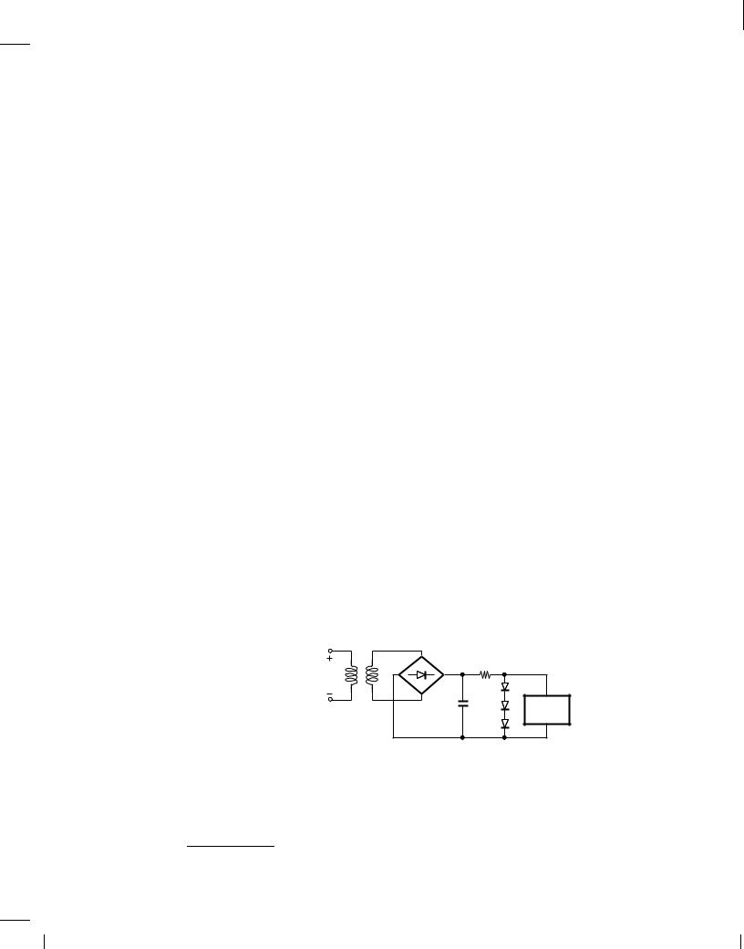
3.5.2 Voltage Regulation
The adaptor circuit studied above generally proves inadequate. Due to the significant variation of the line voltage, the peak amplitude produced by the transformer and hence the dc output vary considerably, possibly exceeding the maximum level that can be tolerated by the load (e.g., a cellphone). Furthermore, the ripple may become seriously objectionable in many applications. For example, if the adaptor supplies power to a stereo, the 120-Hz ripple can be heard from the speakers. Moreover, the finite output impedance of the transformer leads to changes in Vout if the current drawn by the load varies. For these reasons, the circuit of Fig. 3.40(a) is often followed by a “voltage regulator” so as to provide a constant output.
We have already encountered a voltage regulator without calling it such: the circuit studied in Example 3.17 provides a voltage of 2.4 V, incurring only an 11-mV change in the output for a 100-mV variation in the input. We may therefore arrive at the circuit shown in Fig. 3.43 as a more versatile adaptor having a nominal output of 3VD;on 2:4 V. Unfortunately, as studied in Example 3.22, the output voltage varies with the load current.
Diode |
|
Bridge |
|
R1 |
|
Vin |
|
C1 |
Load |
|
Figure 3.43 Voltage regulator block diagram.
Figure 3.44(a) shows another regulator circuit employing a Zener diode. Operating in the reverse breakdown region, D1 exhibits a small-signal resistance, rD, in the range of 1 to 10 , thus providing a relatively constant output despite input variations if rD R1. This can be seen from the small-signal model of Fig. 3.44(b):
This section can be skipped in a first reading.