

Fundamentals of Microelectronics
.pdfBR |
Wiley/Razavi/Fundamentals of Microelectronics [Razavi.cls v. 2006] |
June 30, 2007 at 13:42 |
161 (1) |
|
|
|
|
Sec. 4.7 |
Chapter Summary |
161 |
VCC |
|
|
|
|
|
|
|
|
|
|
|
R C1 |
|
|
|
|
|
|
|
|
|
|
|
|
|
|
|
|
|
R C |
r π 2 |
vπ 2 |
gm2vπ2 |
|
|
Q 1 |
|
Q 2 |
|
|
|
|
r O2 |
||||
v in |
|
|
v in |
r π 1 |
vπ 1 |
gm1vπ1 |
r O1 |
|
|
|
v out |
R |
C2 |
v out |
|
|
|
|
|
|
R |
C2 |
|
|
|
|
|
|
|
|
|
|
|||
(a) |
(b) |
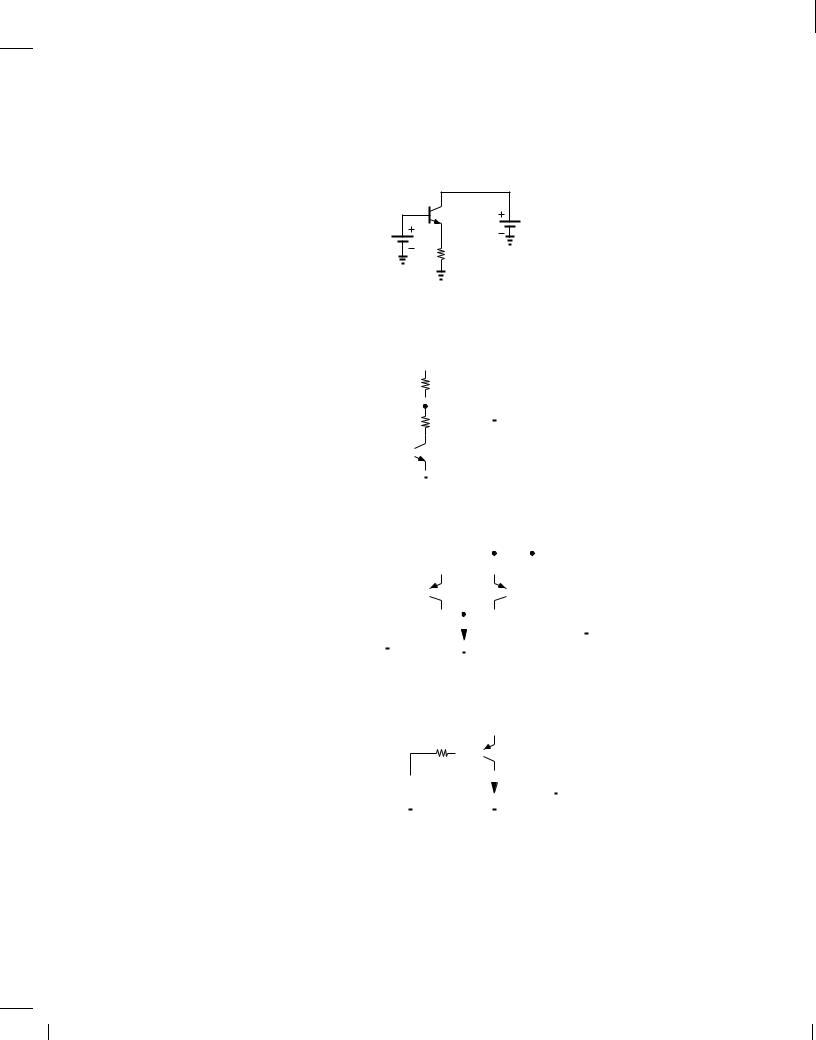
Figure 4.46 (a) Stage using npn and pnp devices, (b) small-signal equivalent of (a).
Solution
Figure 4.46(b) depicts the equivalent circuit. Note that rO1, RC1, and r 2 appear in parallel. Such observations simplify the analysis (Chapter 5).
Exercise
Show that the circuit depicted in Fig. 4.47 has the same small-signal model as the above amplifier.
VCC
RD
R C1 
 v out
v out

 Q 2
Q 2


 Q 1
Q 1
v in
Figure 4.47 Stage using two npn devices.
4.7 Chapter Summary
A voltage-dependent current source can form an amplifier along with a load resistor. Bipolar transistors are electronic devices that can operate as voltage-dependent current sources.
The bipolar transistor consists of two pn junctions and three terminals: base, emitter, and collector. The carriers flow from the emitter to the collector and are controlled by the base.
For proper operation, the base-emitter junction is forward-biased and the base-collector junction reverse-biased (forward active region). Carriers injected by the emitter into the base approach the edge of collector depletion region and ae swept away by the high electric field.

BR |
Wiley/Razavi/Fundamentals of Microelectronics [Razavi.cls v. 2006] |
June 30, 2007 at 13:42 |
162 (1) |
|
|
|
|
162 |
Chap. 4 |
Physics of Bipolar Transistors |
The base terminal must provide a small flow of carriers, some of which go to the emitter and some others recombine in the base region. The ratio of collector current and the base current is denoted by .
In the forward active region, the bipolar transistor exhibits an exponential relationship between its collector current and base-emitter voltage.
In the forward active region, a bipolar transistor behaves as constant current source.
The large-signal model of the bipolar transistor consists of an exponential voltage-dependent current source tied between the collector and emitter, and a diode (accounting for the base current) tied between the base and emitter.
The transconductance of a bipolar transistor is given by gm = IC=VT and remains independent of the device dimensions.
The small-signal model of bipolar transistors consists of a linear voltage-dependent current source, a resistance tied between the base and emitter, and an output resistance.
If the base-collector junction is forward-biased, the bipolar transistor enters saturation and its performance degrades.
The small-signal models of npn and pnp transistors are identical.
Problems
In the following problems, unless otherwise stated, assume the bipolar transistors operate in the active mode.
1.Suppose the voltage-dependent current source of Fig. 4.1(a) is constructed with K = 20 mA/V. What value of load resistance in Fig. 4.1(b) is necessary to achieve a voltage gain of 15?
2.A resistance of RS is placed in series with the input voltage source in Fig. 4.2. Determine
Vout=Vin.
3.Repeat Problem 2 but assuming that rin and K are related: rin = a=x and K = bx. Plot the voltage gain as a function of x.
4.Due to a manufacturing error, the base width of a bipolar transistor has increased by a factor of two. How does the collector current change?
5.In the circuit of Fig. 4.48, it is observed that the collector currents of Q1 and Q2 are equal
I C1 |
I C2 |
Q 1 |
Q 2 |
VBE1 |
VBE2 |
Figure 4.48
if VBE1 , VBE2 = 20 mV. Determine the ratio of transistor cross section areas if the other device parameters are identical.
6.In the circuit of Fig. 4.49, IS1 = IS2 = 3 10,16 A.
(a)Calculate VB such that IX = 1 mA.
(b)With the value of VB found in (a), choose IS3 such that IY = 2:5 mA.
7.Consider the circuit shown in Fig. 4.50.
(a)If IS1 = 2IS2 = 5 10,16 A, determine VB such that IX = 1:2 mA.

BR |
Wiley/Razavi/Fundamentals of Microelectronics [Razavi.cls v. 2006] |
June 30, 2007 at 13:42 |
163 (1) |
|
|
|
|
Sec. 4.7 |
Chapter Summary |
|
|
|
|
163 |
||
|
|
|
|
I X |
|
|
I Y |
|
|
|
|
|
|
|
|||
|
|
|
|
|||||
|
|
|
|
|
|
|
|
|
|
Q 1 |
|
Q 2 |
|
Q 3 |
|
|
|
|
|
|
|
|||||
VB
Figure 4.49
R C |
VCC |
= 2.5 V |
|
I X |
|||
|
|
||
Q 1 Q 2 |
|
|
VB
Figure 4.50
(b) What value of RC places the transistors at the edge of the active mode?
8.Repeat Problem 7 if VCC is lowered to 1.5 V.
9.Consider the circuit shown in Fig. 4.51. Calculate the value of VB that places Q1 at the edge
R C 500 Ω
 VCC = 2 V

 Q 1
Q 1
VB
Figure 4.51
of the active region. Assume IS = 5 10,16 A.
10. In the circuit of Fig. 4.52, determine the maximum value of VCC that places Q1 at the edge of saturation. Assume IS = 3 10,16 A.
R C |
1 kΩ |
|
VCC = 2 V |
R1
 Q 1
Q 1
10 k Ω
Figure 4.52
11.Calculate VX in Fig. 4.53 if IS = 6 10,16 A.
12.An integrated circuit requires two current sources: I1 = 1 mA and I2 = 1:5 mA. Assuming that only integer multiples of a unit bipolar transistor having IS = 3 10,16 A can be placed in parallel, and only a single voltage source, VB, is available (Fig. 4.54), construct

BR |
Wiley/Razavi/Fundamentals of Microelectronics [Razavi.cls v. 2006] |
June 30, 2007 at 13:42 |
164 (1) |
|
|
|
|
164 |
|
|
Chap. 4 |
Physics of Bipolar Transistors |
|
|
Q 1 |
VCC |
= 2 V |
|
|
X |
||
|
1.5 V |
|
|
|
|
1 kΩ |
|
|
|
|
|
|
|
|
|
Figure 4.53 |
|
|
|
|
|
I 1 |
|
I 2 |
VB
Unit
Transistor
Figure 4.54
the required circuit with minimum number of unit transistors.
13.Repeat Problem 12 for three current sources I1 = 0:2 mA, I2 = 0:3 mA, and I3 = 0:45 mA.
14.Consider the circuit shown in Fig. 4.55, assuming = 100 and IS = 7 10,16 A. If
R1 = 10 k , determine VB such that IC = 1 mA.
I C
R1

 Q 1
Q 1
VB
Figure 4.55
15. In the circuit of Fig. 4.55, VB = 800 mV and RB = 10 k . Calculate the collector current.
16. In the circuit depicted in Fig. 4.56, IS1 = 2IS2 = 4 10,16 A. If 1 = 2 = 100 and
|
|
|
|
|
|
|
|
|
|
|
|
|
|
I X |
|
|
I Y |
|
||||||||||||
|
VB |
|
|
|
|
|
|
|
|
|
|
R1 |
|
|
|
|
|
Q 1 |
|
|
|
|
|
Q 2 |
||||||
|
|
|
|
|
|
|
|
|
|
|
|
|
|
|
|
|||||||||||||||
|
|
|
|
|
|
|
|
|
|
|
|
|
|
|
|
|
|
|
|
|
|
|
|
|||||||
|
|
|
|
|
|
|
|
|
|
|
|
|
|
|
|
|
|
|
|
|
|
|
|
|
|
|
|
|
|
|
|
|
|
|
|
|
|
|
|
|
|
|
|
|
|
|
|
|
|
|
|
|
|
|
|
|
|
|
|
|
|
|
|
|
|
|
|
|
|
|
|
|
|
|
|
|
|
|
|
|
|
|
|
|
|
|
|
|
|
|
|
|
|
|
|
|
|
|
|
|
|
|
|
|
|
|
|
|
|
|
|
|
|
|
|
||||||||
|
|
|
|
|
|
|
|
|
|
|||||||||||||||||||||
Figure 4.56 |
|
|
|
|
|
|
|
|
||||||||||||||||||||||
R1 |
= 5 k , compute VB such that IX = 1 mA. |
|
|
|
|
|
|
|
|
|||||||||||||||||||||
17. In the circuit of Fig. 4.56, IS1 = 3 10,16 A, IS2 |
= 5 10,16 A, 1 = 2 = 100, |
|||||||||||||||||||||||||||||
R1 |
= 5 k , and VB = 800 mV. Calculate IX and IY . |
|
|
|
|
|
|
|
|
|||||||||||||||||||||
18.The base-emitter junction of a transistor is driven by a constant voltage. Suppose a voltage source is applied between the base and collector. If the device operates in the forward active

BR |
Wiley/Razavi/Fundamentals of Microelectronics [Razavi.cls v. 2006] |
June 30, 2007 at 13:42 |
165 (1) |
|
|
|
|
Sec. 4.7 |
Chapter Summary |
165 |
region, prove that a change in base-collector voltage results in no change in the collector and base currents. (Neglect the Early effect.)
19.A transistor with IS = 6 10,16 A must provide a transconductance of 1=(13 ). What base-emitter voltage is required?
20.Most applications require that the transconductance of a transistor remain relatively constant as the signal level varies. Of course, since the signal changes the collector current, gm =
IC =VT does vary. Nonetheless, proper design ensures negligible variation, e.g., 10%. If a bipolar device is biased at IC = 1 mA, what is the largest change in VBE that guarantees only 10% variation in gm?
21.Determine the operating point and the small-signal model of Q1 for each of the circuits shown in Fig. 4.57. Assume IS = 8 10,16 A, = 100, and VA = 1.
R C 50 Ω |
|
|
R C 1 kΩ |
R C 1 kΩ |
VCC |
= 2.5 V |
µ A |
VCC = 2.5 V |
VCC = 2.5 V |
|
10 |
|
|
|
Q 1 |
|
|
Q 1 |
Q 1 |
0.8 V |
|
|
|
|
(a) |
|
|
(b) |
(c) |
Figure 4.57
22.Determine the operating point and the small-signal model of Q1 for each of the circuits shown in Fig. 4.58. Assume IS = 8 10,16 A, = 100, and VA = 1.
10 µ A |
|
|
|
|
|
|
|
|
Q 1 |
|
|
|
|
|
|
|
|
|
|
|
VCC = 2 V |
|
|
|
|
|
|
Q 1 |
|
|
|
|
|
|
|
|
|
|
|
|
VCC = 2 V |
|||||||||||||||||
|
|
|
|
|
|
|
|
|
|
|
|
|
|
|
|
|
|
|
|
|
|
|
|
|
|
|
|
|
|
|
|
|
|
|
|
|
||||||||||||||||||||||
|
|
|
|
|
|
|
|
|
|
|
|
|
|
|
|
|
|
|
|
|
|
|
|
|
|
|
|
|
|
|
|
|
|
|
|
|
||||||||||||||||||||||
|
|
|
|
|
|
|
|
|
|
|
1 kΩ |
|
|
|
|
|
|
|
|
|
|
|
1 kΩ |
|
|
|
|
|
|
|||||||||||||||||||||||||||||
|
|
|
|
|
|
|
|
|
|
|
|
|
|
|
|
|
|
|
|
|
|
|
|
|
|
|
|
|||||||||||||||||||||||||||||||
|
|
|
|
|
|
|
|
|
|
|
|
|
|
|
|
|
|
|
|
|
|
|
|
|
|
|
|
|||||||||||||||||||||||||||||||
|
|
|
|
|
|
|
|
|
|
|
|
|
|
|
|
|
|
|
|
|
|
|
|
|
|
|
|
|
|
|
|
|
|
|
|
|
|
|
|
|
|
|
|
|
|
|
|
|
|
|
|
|
|
|
|
|
|
|
|
|
|
|
|
|
|
|
|
|
|
|
|
|
|
|
|
|
|
|
|
|
|
|
|
|
|
|
|
|
|
|
|
|
|
|
|
|
|
|
|
|
|
|
|
|
|
|
|
|
|
|
|
||||||
|
|
|
|
|
|
(a) |
|
|
|
|
|
|
(b) |
|
|
|
|
|
|
|||||||||||||||||||||||||||||||||||||||
|
|
|
|
|
|
|
|
|
|
|
|
|
|
|
|
|
|
|
|
|
|
|
|
|
VCC = 2 V |
|
|
|
|
|
|
|
|
|
|
|
|
|
|
|
|
|
|
|
VCC = 2 V |
|||||||||||||
|
|
|
|
|
|
Q 1 |
|
|
|
|
|
|
|
|
|
|
|
|
|
|
|
|
|
|
|
|
|
|
1 mA |
|
|
|
|
|
|
|
|
|
||||||||||||||||||||
|
|
|
|
|
|
|
|
|
|
|
|
|
|
|
|
|
|
|
|
|
|
|
|
|
|
|
|
|
|
|
|
|
|
|
|
|
||||||||||||||||||||||
|
|
|
|
|
|
|
|
|
|
|
|
|
|
|
|
|
|
|
|
|
|
|
|
|
|
|
|
|
|
|
|
|
|
|
|
|
|
|
|
|
|
|
|
|
|
|
|
|
|
|
|
|
||||||
|
|
|
|
|
|
|
|
|
|
1 mA |
|
|
|
|
|
|
|
|
|
Q 1 |
|
|
|
|
|
|
||||||||||||||||||||||||||||||||
|
|
|
|
|
|
|
|
|
|
|
|
|
|
|
|
|
|
|
|
|
|
|
|
|
||||||||||||||||||||||||||||||||||
|
|
|
|
|
|
|
|
|
|
|
|
|
|
|
|
|
|
|
|
|
|
|
|
|
||||||||||||||||||||||||||||||||||
|
|
|
|
|
|
|
|
|
|
|
|
|
|
|
|
|
|
|
|
|
|
|
|
|
||||||||||||||||||||||||||||||||||
|
|
|
|
|
|
|
|
|
|
|
|
|
|
|
|
|
|
|
|
|
|
|
|
|
|
|
|
|
|
|
|
|
|
|
|
|
|
|
|
|
|
|
|
|
|
|
|
|
|
|
|
|
|
|
|
|
|
|
|
|
|
|
|
|
|
|
|
|
|
|
|
|
|
|
|
|
|
|
|
|
|
|
|
||||||||||||||||||||||||||||||||||
|
|
|
(c) |
|
|
|
|
|
|
(d) |
|
|
|
|
|
|
||||||||||||||||||||||||||||||||||||||||||
Figure 4.58 |
|
|
|
|
|
|
|
|
|
|
|
|
|
|
|
|
|
|
|
|
|
|
|
|
|
|
|
|
|
|
|
|
|
|
|
|
|
|
|
|
|
|
|
|
|
|
|
|
|
|
|
|
|
|
|
|
|
|
23. A fictitious bipolar transistor exhibits an |
IC-VBE characteristic given by |
|
|
|
|
|
|
|||||||||||||||||||||||||||||||||||||||||||||||||||
|
|
|
|
|
|
|
|
|
|
|
|
|
|
|
|
|
|
|
|
|
|
|
|
|
|
|
I |
= I |
S |
exp VBE |
; |
|
|
|
|
|
|
|
|
|
|
|
|
|
|
|
|
|
|
|
|
(4.119) |
||||||
|
|
|
|
|
|
|
|
|
|
|
|
|
|
|
|
|
|
|
|
|
|
|
|
|
|
|
|
C |
|
nVT |
|
|
|
|
|
|
|
|
|
|
|
|
|
|
|
|
|
|
|
|
|
|
|
|
|
|
|
|
|
|
|
|
|
|
|
|
|
|
|
|
|
|
|
|
|
|
|
|
|
|
|
|
|
|
|
|
|
|
|
|
|
|
|
|
|
|
|
|
|
|
|
|
|
|
|
|
|
|
|
|
|
|
|
|
|
|
|
where n is a constant coefficient. Construct the small-signal model of the device if IC is still equal to IB.

BR |
Wiley/Razavi/Fundamentals of Microelectronics [Razavi.cls v. 2006] |
June 30, 2007 at 13:42 |
166 (1) |
|
|
|
|
166 |
Chap. 4 |
Physics of Bipolar Transistors |
24.A fictitious bipolar transistor exhibits the following relationship between its base and collector currents:
I |
= aI2 ; |
(4.120) |
C |
B |
|
where a is a constant coefficient. Construct the small-signal model of the device if |
IC is still |
|
equal to IS exp(VBE=VT ). |
|
|
25.The collector voltage of a bipolar transistor varies from 1 V to 3 V while the base-emitter voltage remains constant. What Early voltage is necessary to ensure that the collector current changes by less than 5%?
26. |
In the circuit of Fig. 4.59, IS = 5 10,17 A. Determine VX for (a) VA = 1, and (b) |
||||||||||||||||||||||||||
|
|
|
|
|
|
|
|
|
|
|
|
|
|
|
|
|
|
|
|
|
|
|
|
||||
|
|
|
|
|
|
|
|
|
|
R C |
|
|
|
|
1 kΩ |
|
|
|
|
|
|
|
|
||||
|
|
|
|
|
|
|
|
|
|
|
|
|
|
|
|
|
|
|
|
|
|
||||||
|
|
|
|
|
|
|
|
|
|||||||||||||||||||
|
|
|
|
|
|
|
|
|
|
|
|
|
|
|
X |
|
|
|
|
|
|
|
|
|
|
VCC = 2.5 V |
|
|
|
|
|
|
|
|
|
|
|
|
|
|
|
|
|
|
|
|
|
|
|
|
|
|
|||
|
|
|
|
|
|
|
|
|
|
|
|
|
|
|
|
|
|
|
|
|
|
|
|
|
|||
|
|
|
|
|
|
|
|
|
|
|
|
|
|
|
|
|
|
|
|
|
|
|
|
|
|
||
|
|
|
|
|
|
|
|
|
|
|
|
|
|
|
|
|
|
|
|
|
|||||||
|
|
|
|
|
|
|
|
|
|
|
|
|
|
|
|
|
|
|
|
|
|
|
|||||
|
VB = 0.8 V |
|
|
|
|
|
|
|
|
|
|
|
|
Q 1 |
|||||||||||||
|
|
|
|
|
|
|
|
|
|
|
|
|
|||||||||||||||
|
|
|
|
|
|
|
|
|
|
|
|
|
|||||||||||||||
|
|
|
|
|
|
|
|
|
|
|
|
|
|
|
|
|
|
|
|
|
|
|
|
|
|
||
|
|
|
|
|
|
|
|
|
|
|
|
|
|
|
|
|
|
|
|
|
|
|
|
||||
|
|
|
|
|
|
|
|
|
|
|
|
|
|
|
|
|
|
|
|
|
|
|
|
||||
|
|
|
|
|
|
|
|
|
|
|
|
|
|
|
|
|
|
|
|
|
|
|
|
|
|||
|
|
|
|
|
|
|
|
|
|
|
|
|
|
|
|
|
|
|
|
|
|
|
|
|
|
|
|
|
|
|
|
|
|
|
|
|
|
|
|
|
|
|
|
|
|
|
|
|
|
|
|
|
|
|
|
|
|
|
|
|
|
|
|
|
|
|
|
|
|
|
|
|
|
|
|
|
|
|
|
|
|
|
|
|
|
|
|
|
|
|
|
|
|
|
|
|
|
|
|
|
|
|
|
|
|
|
|
|
|
||
Figure 4.59 |
|
|
|
|
|
|
|
|
|
|
|
|
|
|
|
|
|||||||||||
|
VA = 5 V. |
|
|
|
|
|
|
|
|
|
|
|
|
|
|
|
|
||||||||||
27. |
In the circuit of Fig. 4.60, VCC changes from 2.5 to 3 V. Assuming IS = 1 10,17 A and |
||||||||||||||||||||||||||
|
|
|
|
|
|
|
|
|
|
|
|
|
|
|
|
|
|
|
|||||||||
|
|
|
|
|
|
|
|
|
|
R C |
|
|
|
|
2 kΩ |
|
|
|
|||||||||
|
|
|
|
|
|
|
|
|
|
|
|
|
|
|
|
|
|||||||||||
|
|
|
|
|
|
|
|
|
|
|
|
|
|
||||||||||||||
|
|
|
|
|
|
|
|
|
|
|
|
|
|
|
|
|
|
|
|
|
|
|
|
|
|
|
VCC |
|
|
|
|
|
|
|
|
|
|
|
|
|
|
|
|
|
|
|
|
|
|
|
|
|
|
|
|
|
|
|
|
|
|
|
|
|
|
|
|
|
|
|
|
|
|
|
|
|
|
|
|
|
|
|
|
|
|
|
|
|
|
|
|
|
|
|
|
|
|
|
|
|
|
|
|
|
|
|
|
|
|
|
|
|
|
|
|
|
|
|
|
|
|
|
|
|
|
|
|
|
|
|
|
|
|
|
|
|
|
|
|
|
|
|
|
|
|
|
|
|
|
|
|
|
|
|
|
|
|
|
|
|
|
|
|
|
|
|
|

 Q 1
Q 1
0.8 V
Figure 4.60
VA = 5 V, determine the change in the collector current of Q1.
28.In Problem 27, we wish to decrease VB to compensate for the change in IC . Determine the new value of VB.
29.Consider the circuit shown in Fig. 4.61, where I1 is a 1-mA ideal current source and IS =
3 10,17 A.
I 1 |
VCC |
= 2 V |
|

 Q 1
Q 1
VB
Figure 4.61
(a)Assuming VA = 1, determine VB such that IC = 1 mA.
(b)If VA = 5 V, determine VB such that IC = 1 mA for a collector-emitter voltage of 1.5 V.

BR |
Wiley/Razavi/Fundamentals of Microelectronics [Razavi.cls v. 2006] |
June 30, 2007 at 13:42 |
167 (1) |
|
|
|
|
Sec. 4.7 |
Chapter Summary |
167 |
30.A bipolar current source is designed for an output current of 2 mA. What value of VA guarantees an output resistance of greater than 10 k .
31.In the circuit of Fig. 4.62, n identical transistors are placed in parallel. If IS = 5 10,16 A
VB = 0.8 V 
Figure 4.62
and VA = 8 V for each device, construct the small-signal model of the equivalent transistor.
32. Consider the circuit shown in Fig. 4.63, where IS = 6 10,16 A and VA = 1.
R C 2 kΩ
 VCC = 2.5 V

 Q 1
Q 1
VB
Figure 4.63
(a)Determine VB such that Q1 operates at the edge of the active region.
(b)If we allow soft saturation, e.g., a collector-base forward bias of 200 mV, by how much can VB increase?
33.For the circuit depicted in Fig. 4.64, calculate the maximum value of VCC that produces a
R C 1 kΩ
 VCC
VCC

 Q 1
Q 1
Figure 4.64
collector-base forward bias of 200 mV. Assume IS = 7 10,16 A and VA = 1.
34.Assume IS = 2 10,17 A, VA = 1, and = 100 in Fig. 4.65. What is the maximum value of RC if the collector-base must experience a forward bias of less than 200 mV?
100 k Ω RB |
RC |
|
VCC = 2.5 V |
|
Q 1 |
Figure 4.65
BR |
Wiley/Razavi/Fundamentals of Microelectronics [Razavi.cls v. 2006] |
June 30, 2007 at 13:42 |
168 (1) |
|
|
|
|
168 |
Chap. 4 |
Physics of Bipolar Transistors |
35.Consider the circuit shown in Fig. 4.66, where IS = 5 10,16 A and VA = 1. If VB is chosen to forward-bias the base-collector junction by 200 mV, what is the collector current?
Q 1 |
VCC |
= 2.5 V |
|
VB |
|||
|
|
||
1 kΩ |
|
|
Figure 4.66
36.In the circuit of Fig. 4.67, = 100 and VA = 1. Calculate the value of IS such that the base-collector junction is forward-biased by 200 mV.
|
|
|
|
|
|
|
|
|
|
|
R C |
|
|
|
9 kΩ |
|
|
|
|
|
|
|
|
|
|
|
|
VCC = 2.5 V |
|
|||||||||||||||||||||||||||||||||
|
|
|
|
|
|
|
|
|
|
|
|
|
|
|
|
|
|
|
|
|
|
|
|
|
|
|
||||||||||||||||||||||||||||||||||||
|
|
|
|
|
|
|
|
|
|
|
R p |
|
|
|
1 kΩ |
|
|
|
|
|
|
|
|
|
|
|
|
|
|
|
|
|
|
|
|
|
|
|
|
|
|
|
|
|
|
|
|
|
|
|
|
|||||||||||
|
|
|
|
|
|
|
|
|
|
|
|
|
|
|
|
|
|
|
|
|
|
|
|
|
|
|
|
|
|
|
|
|
|
|
|
|
|
|
|
|
|
|
|
|
||||||||||||||||||
|
|
|
|
|
|
|
|
|
|
|
|
|
|
|
|
|
|
|
|
|
Q 1 |
|
|
|
|
|
|
|
|
|
|
|
|
|
|
|
|
|
|
|
|
|
|
|
|
|
|
|
|
|
|
|
|
|
|
|
|
|||||
|
|
|
|
|
|
|
|
|
|
|
|
|
|
|
|
|
|
|
|
|
|
|
|
|
|
|
|
|
|
|
|
|
|
|
|
|
|
|
|
|
|
|
|
|
|
|
|
|
|
|
|
|
|
|
|
|
||||||
|
|
|
|
|
|
|
|
|
|
|
|
|
|
|
|
|
|
|
|
|
|
|
|
|
|
|
|
|
|
|
|
|
|
|
|
|
|
|
|
|
|
|
|
|
|
|
|
|
|
|
|
|
|
|
|
|
||||||
|
|
|
|
|
|
|
|
|
|
|
|
|
|
|
|
|
|
|
|
|
|
|
|
|
|
|
|
|
|
|
|
|
|
|
|
|
|
|
|
|
|
|
|
|
|
|
|
|
|
|
|
|
|
|
||||||||
Figure 4.67 |
|
|
|
|
|
|
|
|
|
|
|
|
|
|
|
|
|
|
|
|
|
|
|
|
|
|
|
|
|
|
|
|
|
|
|
|
|
|
|
|
|
|
|
|
||||||||||||||||||
|
|
|
|
|
|
|
|
|
|
|
|
|
|
|
|
|
|
|
|
|
|
|
|
|
|
|
|
|
|
|
|
|
|
|
|
|
|
|
|
|
|
|
|
|||||||||||||||||||
|
|
|
|
|
|
|
|
|
|
|
|
|
|
|
|
|
|
|
|
|
|
|
|
|
|
|
|
|
|
|
|
|
|
|
|
|
|
|
|
|
|
|
|
|||||||||||||||||||
|
|
|
|
|
|
|
|
|
|
|
|
|
|
|
|
|
|
|
|
|
|
|
|
|
|
|
|
|
|
|
|
|
|
|
|
|
|
|
|
|
|
|
|
|||||||||||||||||||
37. |
If IS1 = 3IS2 = 6 10,16 A, calculate IX in Fig. 4.68. |
|
|
|
|
|
|
|
|
|
|
|
|
|
|
|||||||||||||||||||||||||||||||||||||||||||||||
|
|
|
|
|
|
|
|
|
|
|
|
|
|
|
|
|
|
|
|
|
|
|
|
|
|
|
|
|
|
|
|
|
|
|
|
|
|
|
|
|
|
|
|
|
|
|
|
|
|
|
|
|
|
|
|
|
|
|
|
|
|
|
|
|
|
|
|
|
|
|
|
|
|
|
|
|
|
|
|
|
|
|
|
|
|
|
|
|
|
|
|
|
|
|
|
|
|
|
|
|
|
|
|
|
|
|
|
|
|
|
|
0.82 V |
|
|
|
||||||||||
|
|
|
|
|
|
|
|
|
|
|
|
|
|
|
|
|
|
|
|
|
|
|
Q 1 |
|
|
Q 2 |
|
|
|
|
|
|
|
|
|
|
|
|
|
|||||||||||||||||||||||
|
|
|
|
|
|
|
|
|
|
|
|
|
|
|
|
|
|
|
|
|
|
|
|
|
|
|
|
|
|
|
|
|
|
|
|
|
|
|
|
|
|
|
|
|
|
|
|
|
||||||||||||||
|
1.7 V |
|
|
|
|
|
|
|
|
|
|
|
|
|
|
|
|
|
|
|
|
|
|
|
|
|
|
|
|
|
|
|
|
|
|
|
|
|
|
|
|
|
|
|
|
|
|
|
|
|
|
|
VCC |
|
|
|
2 V |
|||||
|
|
|
|
|
|
|
|
|
|
|
|
|
|
|
|
|
|
|
|
|
|
|
|
|
|
|
|
|
|
|
|
|
|
|
|
|
|
|
|
|
|
|
|
|
|
|
|
|
|
|
||||||||||||
|
|
|
|
|
|
|
|
|
|
|
|
|
|
|
|
|
|
|
|
|
|
|
|
|
|
I X |
|
|
|
|
|
|
|
|
|
|
|
|
|
|
||||||||||||||||||||||
|
|
|
|
|
|
|
|
|
|
|
|
|
|
|
|
|
|
|
|
|
|
|
|
|
|
|
|
|
|
|
||||||||||||||||||||||||||||||||
|
|
|
|
|
|
|
|
|
|
|
|
|
|
|
|
|
|
|
|
|
|
|
|
|
|
|
|
|
|
|
|
|
|
|
|
|
|
|
|
|
|
|
||||||||||||||||||||
|
|
|
|
|
|
|
|
|
|
|
|
|
|
|
|
|
|
|
|
|
|
|
|
|
|
|
|
|
|
|
|
|
|
|
|
|
|
|
|
|
|
|
|
|
|
|
|
|
|
|
|
|
|
|
||||||||
Figure 4.68 |
|
|
|
|
|
|
|
|
|
|
|
|
|
|
|
|
|
|
|
|
|
|
|
|
|
|
|
|
|
|
|
|
|
|
|
|
|
|
|
|
|
|
|
|
||||||||||||||||||
|
|
|
|
|
|
|
|
|
|
|
|
|
|
|
|
|
|
|
|
|
|
|
|
|
|
|
|
|
|
|
|
|
|
|
|
|
|
|
|
|
|
|
|
|||||||||||||||||||
38. |
Determine the collector current of Q1 in Fig. 4.69 if IS = 2 10,17 A and = 100. |
|||||||||||||||||||||||||||||||||||||||||||||||||||||||||||||
|
|
|
|
|
|
|
|
|
|
|
|
|
|
|
|
|
|
|
|
|
|
50 k Ω |
|
|
|
|
|
|
|
|
|
|
|
|
|
|
|
|
|
|
|
|
|
|
|
|
|
|
|
|
|
|
|
|
|
|
|
|
||||
|
|
|
|
|
|
|
|
|
|
|
|
|
|
|
|
|
|
|
|
|
|
|
|
|
|
|
|
|
|
Q 1 |
|
|
|
|
|
|
|
|
|
|
|
|
|
|
||||||||||||||||||
|
|
|
|
|
|
|
|
|
|
|
|
|
|
|
|
|
|
|
|
|
|
|
|
|
|
|
|
|
|
|
|
|
|
|
|
|
|
|
|
|
|
|
|
|||||||||||||||||||
|
|
|
|
|
|
|
|
|
|
|
|
|
|
|
|
|
|
|
|
|
|
|
|
|
|
|
|
|
|
|
|
|
|
|
|
|
|
|
|
|
|
|
|
|
|
|
|
|
||||||||||||||
|
|
|
|
|
|
|
|
|
|
|
|
|
|
|
|
|
|
|
|
|
|
RB |
|
|
|
|
|
|
|
|
|
|
|
|
|
|
|
|
|
|
|
|
|
|
||||||||||||||||||
|
1.7 V |
|
|
|
|
|
|
|
|
|
|
|
|
|
|
|
|
|
|
|
|
|
|
|
|
|
VCC |
|
|
|
|
|
|
|
|
|
2 V |
|
||||||||||||||||||||||||
|
|
|
|
|
|
|
|
|
|
|
|
|
|
|
|
|
|
|
|
|
|
|
|
|
|
|
|
|
|
|
|
|
|
|
|
|||||||||||||||||||||||||||
|
|
|
|
|
|
|
|
|
|
|
|
|
|
|
|
|
|
|
|
|
|
|
|
|
|
|
I C |
|
|
|
|
|
|
|
|
|
|
|
|
|
|
|||||||||||||||||||||
|
|
|
|
|
|
|
|
|
|
|
|
|
|
|
|
|
|
|
|
|
|
|
|
|
|
|
|
|
|
|
|
|
|
|
|
|
|
|
|
|
|
|
|
|
|
|
|
|
|
|
|
|
|
|
|
|
|
|
|
|
|
|
Figure 4.69
39.In the circuit of Fig. 4.70, it is observed that IC = 3 mA. If = 100, calculate IS.
40.Determine the value of IS in Fig. 4.71 such that Q1 operates at the edge of the active mode.
41.What is the value of that places Q1 at the edge of the active mode in Fig. 4.72? Assume
IS = 8 10,16 A.
42.Calculate the collector current of Q1 in Fig. 4.73 if IS = 3 10,17 A.

BR |
Wiley/Razavi/Fundamentals of Microelectronics [Razavi.cls v. 2006] |
June 30, 2007 at 13:42 |
169 (1) |
|
|
|
|
Sec. 4.7 |
Chapter Summary |
|
|
|
|
|
|
|
|
|
|
|
|
|
|
|
|
|
|
|
|
|
|
|
|
|
|
|
|
|
|
|
|
|
|
|
|
|
|
|
169 |
|||||||||||||||||||||
|
|
|
|
|
|
|
|
|
23 k Ω |
|
|
|
|
|
|
|
|
|
|
|
|
|
|
|
|
|
|
|
|
|
|
|
|
|
|
|
|
|
|
|
|
|
|
|
|
|
|
|
|
|||||||||||||
|
|
|
|
|
|
|
|
|
Q 1 |
|
|
|
|
|
|
|
|
|
|
|
|
|
|
|
|
|
||||||||||||||||||||||||||||||||||||
|
|
|
|
|
|
|
|
|
|
|
|
|
|
|
|
|
|
|
|
|
|
|
|
|
|
|||||||||||||||||||||||||||||||||||||
|
|
|
|
|
|
|
|
|
|
|
|
|
|
|
|
|
|
|
|
|
|
|
|
|
|
|
|
|
|
|
|
|
|
|
|
|
|
|
|
|
|
|
|
|
|
|
||||||||||||||||
|
|
|
|
|
|
|
|
|
|
|
RB |
|
|
|
|
|
|
|
|
|
|
|
|
|
|
|
|
|
|
|||||||||||||||||||||||||||||||||
|
|
|
|
|
|
|
|
|
|
|
|
|
|
|
|
|
|
|
|
|
|
|
|
|
|
|
|
|
|
|
|
|
||||||||||||||||||||||||||||||
|
|
|
|
|
|
|
|
|
|
|
|
|
|
|
|
|
|
|
|
|
|
|
VCC |
|
|
|
|
|
|
|
1.5 V |
|
||||||||||||||||||||||||||||||
|
|
|
|
|
|
|
|
|
|
|
|
|
|
|
|
|
|
|
|
|
|
|
||||||||||||||||||||||||||||||||||||||||
Figure 4.70 |
|
|
|
|
|
|
|
|
|
|
|
|
|
|
|
|
|
|
|
|
|
|
|
|
|
|
|
|
|
|
|
|
I C |
|
|
|
|
|
|
|
|
|
|
|
|
|
|
|
|
|||||||||||||
|
|
|
|
|
|
|
|
|
|
|
|
|
|
|
|
|
|
|
|
|
|
|
|
|
|
|
|
|
|
|
|
|
|
|
|
|
|
|
|
|
|
|
|
|||||||||||||||||||
|
|
|
|
|
|
|
|
|
|
|
|
|
|
|
|
|
|
|
|
|
|
|
|
|
|
|
|
|
|
|
|
|
|
|
|
|
|
|
|
|||||||||||||||||||||||
|
|
|
|
|
|
|
|
|
|
|
|
|
|
|
|
|
|
|
|
|
|
|
|
|
|
|
|
|
|
|
|
|
|
|
|
|
|
|
|
|
|
|
|
|
|
|
|
|
|
|
|
|
|
|
|
|
|
|
|
|
|
|
|
|
|
|
|
|
|
|
|
|
|
|
|
|
|
|
|
|
|
|
|
|
|
|
|
|
|
|
|
|
|
|
|
|
|
|
|
|
|
|
|
|
|
|
|
|
|
|
|
|
|
|
|
|
|
|
|
|
|
|
|
|
|
|
|
|
|
|
|
|
|
|
|
|
|
|
|
|
|
|
|
|
|
|
|
|
|
|
|
|
|
|
|
|
|
|
|
|
|
|
|
|
|
|
|
|
|
|
|
|
|
|
|
|
|
|
|
|
|
|
|
|
|
|
|
|
|
|
|
|
|
|
|
|
|
|
|
|
|
|
|
|
|
|
|
|
|
|
|
|
|
|
|
|
|
|
|
|
|
|
|
|
|
|
|
|
|
|
|
|
|
|
|
|
|
|
|
|
|
|
|
|
|
|
|
|
|
||
|
|
|
|
|
|
|
|
|
|
|
|
|
|
|
|
|
|
|
|
|
|
|
|
|
|
|
|
|
|
|
|
|
|
|
|
Q 1 |
|
|
|
|
|
|
|
|
|
|
|
|
|
|
||||||||||||
|
|
|
|
|
|
|
|
|
|
|
|
|
|
|
|
|
|
|
|
|
|
|
|
|
|
|
|
|
|
|
|
|
|
|
|
|
|
|
|
|
|
|
|
|
|
|
|
|
|
|||||||||||||
|
|
|
|
VB = 1.2 V |
|
|
|
|
|
|
|
|
|
|
|
|
|
|
|
|
|
|
|
|
|
|
|
|
|
|
|
|
|
|
|
|
VCC |
|
|
|
|
|
2 V |
|||||||||||||||||||
Figure 4.71 |
|
|
|
|
|
|
|
|
|
|
|
|
|
|
|
|
|
|
|
|
|
|
|
|
|
|
|
|
|
|
|
|
R C |
|
|
|
|
2 kΩ |
|
|
|
|||||||||||||||||||||
|
|
|
|
|
|
|
|
|
|
|
|
|
|
|
|
|
|
|
|
|
|
|
|
|
|
|
|
|
|
|
|
|
||||||||||||||||||||||||||||||
|
|
|
|
|
|
|
|
|
|
|
|
|
|
|
|
|
|
|
|
|
|
|
|
|
|
|
|
|
|
|
|
|
||||||||||||||||||||||||||||||
|
|
|
|
|
|
|
|
|
|
|
|
|
|
|
|
|
|
|
|
|
|
|
|
|
|
|
|
|
|
|
|
|
|
|
|
|
|
|
|
|
|
|
|
|
|
|
|
|
|
|
|
|
|
|
|
|
|
|
|
|
|
|
|
|
|
|
|
|
|
|
|
|
|
|
|
|
|
|
|
|
|
|
|
|
|
|
|
|
|
|
|
|
|
|
|
|
|
|
|
|
|
|
|
|
|
|
|
|
|
|
|
|
|
|
|
|
|
|
|
|
|
|
|
|
|
|
|
|
|
|
|
|
100 k Ω |
|
|
|
|
|
|
|
|
|
|
|
|
|
|
|
|
|
|
|
|
|
|
|
|
|
|
|
|
|
|
|
|
|
|
|
|
|
|
|
|
|||||||||||||||
|
|
|
|
|
|
|
|
|
|
|
|
Q 1 |
|
|
|
|
|
|
|
|
|
|
|
|
|
|
|
|
|
|
|
|
|
|||||||||||||||||||||||||||||
|
|
|
|
|
|
|
|
|
|
|
|
|
|
|
|
|
|
|
|
|
|
|
|
|
|
|
|
|
|
|
|
|
||||||||||||||||||||||||||||||
|
|
|
|
|
|
|
|
|
|
|
|
|
|
|
|
|
|
|
|
|
|
|
|
|
|
|
|
|
|
|
|
|
|
|
|
|
|
|
|
|
|
|
|
|
||||||||||||||||||
|
|
|
|
|
|
|
|
|
RB |
|
|
|
|
|
|
|
|
|
|
|
|
|
|
|
|
|
|
|||||||||||||||||||||||||||||||||||
|
|
|
|
|
|
|
|
|
|
|
|
|
|
|
|
|
|
|
|
|
|
|
|
|
|
|
|
|
||||||||||||||||||||||||||||||||||
|
|
|
|
|
|
|
|
|
|
|
|
|
|
|
|
|
|
|
|
VCC |
|
|
|
|
|
|
|
|
|
|
|
1.5 V |
|
|||||||||||||||||||||||||||||
|
|
|
|
|
|
|
|
|
|
|
|
|
|
|
|
|
|
|
|
|
|
|
|
|
|
|||||||||||||||||||||||||||||||||||||
Figure 4.72 |
|
|
|
|
|
|
|
|
|
|
|
|
|
|
|
|
|
|
|
|
|
|
|
|
|
|
|
|
|
|
|
1 kΩ |
|
|
|
|
|
|
|
|
|
|
|
|
|
|
|
|
|
|
||||||||||||
|
|
|
|
|
|
|
|
|
|
|
|
|
|
|
|
|
|
|
|
|
|
|
|
|
|
|
|
|
|
|
|
|
|
|
|
|
|
|
|
|
|
|
|
|
|
|
||||||||||||||||
|
|
|
|
|
|
|
|
|
|
|
|
|
|
|
|
|
|
|
|
|
|
|
|
|
|
|
|
|
|
|
|
|
|
|
|
|
|
|
|
|
|
|
|
|
|
|
|
|
||||||||||||||
|
|
|
|
|
|
|
|
|
|
|
|
|
|
|
|
|
|
|
|
|
|
|
|
|
|
|
|
|
|
|
|
|
|
|
|
|
|
|
|
|
|
|
|
|
|
|
|
|
|
|
|
|
|
|
|
|
|
|
|
|
|
|
|
|
|
|
|
|
|
|
|
|
|
|
|
|
|
|
|
|
|
|
|
|
|
|
|
|
|
|
|
|
|
|
|
|
|
|
|
|
|
|
|
|
|
|
|
|
|
|
|
|
|
|
|
|
|
|
|
|
|
|
|
|
|
|
|
|
|
|
|
|
|
|
|
|
|
|
|
|
|
|
|
|
|
|
|
|
|
|
|
|
|
|
|
|
|
|
|
|
|
|
|
|
|
|
|
|
|
|
|
|
|
|
|
|
|
|
|
|
|
|
|
|
|
|
|
|
|
|
|
|
|
|
|
|
|
|
1 kΩ |
|
|
|
|
|
|
|
|
|
|
|
|
|
|
|
|
|
|
|
|
|
|
|
|
|
|
|
|
|
|
|
|
|
|
|
|
|
|
|
|
||||||||||||
|
|
|
|
|
|
|
|
|
|
|
|
|
|
|
|
|
|
|
|
|
|
|
|
|
|
|
|
|
|
|
|
|
VCC |
|
|
|
|
|
|
|
|
2.5 V |
|
|||||||||||||||||||
|
|
|
|
|
|
|
|
|
|
|
|
|
|
|
|
|
|
|
|
|
|
|
|
|
|
|
|
|
|
|
|
|
|
|
|
|
|
|
|
|
|
|
|
|
|
|
||||||||||||||||
|
|
|
1 V |
|
|
|
|
|
|
|
|
|
|
|
|
|
|
|
Q 1 |
|
|
|
|
|
|
|
|
|
|
|
|
|
|
|
|
|
||||||||||||||||||||||||||
|
|
|
|
|
|
|
|
|
|
|
|
|
|
|
|
|
|
|
|
|
|
|
|
|
|
|
|
|
|
|
|
|
|
|
|
|
|
|
|
|
|
|
|
|
|
|
|
|
|
|
|
|
|
|
|
|
||||||
|
|
|
|
|
|
|
|
|
|
|
|
|
|
|
|
|
|
|
|
|
|
|
|
|
|
|
|
|
|
|
|
|
|
|
|
|
|
|
|
|
|
|
|
|
|
|
|
|
|
|
|
|
||||||||||
|
|
|
|
|
|
|
|
|
|
|
|
|
|
|
|
|
|
|
|
|
|
|
|
|
|
|
|
|
|
|
|
|
|
|
|
|
|
|
|
|
|
|
|
|
|
|
|
|
|
|
|
|
|
|
|
|
|
|
|
|
|
|
|
|
|
|
|
|
|
|
|
|
|
|
|
|
|
|
|
|
|
|
|
|
|
|
|
|
|
|
|
|
|
|
|
|
|
|
|
|
|
|
|
|
|
|
|
|
|
|
|
|
|
|
|
|
|
|
|
|
|
|
|
|
|
|
|
|
|
|
|
|
|
|
|
|
|
|
|
|
|
|
|
|
|
|
|
|
|
|
|
|
|
|
|
|
|
|
|
|
|
|
|
|
|
|
|
|
|
|
|
|
|
|
|
|
|
|
|
|
|
|
|
|
|
|
|
|
|
|
|
|
|
|
|
|
|
|
|
|
|
|
|
|
|
|
|
|
|
|
|
|
|
|
|
|
|
|
|
|
|
|
|
|
|
|
|
|
|
|
|
|
|
|
|
|
|
|
|
|
|
|
|
|
|
|
|
|
|
|
|
|
|
|
|
|
|
|
|
|
|
|
|
|
|
|
|
|
|
|
|
|
|
|
|
|
|
|
|
|
|
|
|
|
|
|
|
|
|
|
|
|
|
|
|
|
|
|
|
|
|
|
|
|
|
|
|
|
|
|
|
|
|
|
Figure 4.73
43. Determine the operating point and the small-signal model of Q1 for each of the circuits shown in Fig. 4.74. Assume IS = 3 10,17 A, = 100, and VA = 1.
|
Q 1 |
|
|
|
Q 1 |
|
Q 1 |
|
1.7 V |
VCC |
2.5 V |
20 |
µ A |
VCC |
2.5 V |
VCC |
2.5 V |
|
1 kΩ |
|
500 Ω |
|
2 kΩ |
|
||
|
|
|
|
|
|
|||
|
(a) |
|
|
|
(b) |
|
(c) |
|
Figure 4.74
44.Determine the operating point and the small-signal model of Q1 for each of the circuits shown in Fig. 4.75. Assume IS = 3 10,17 A, = 100, and VA = 1.
45.In the circuit of Fig. 4.76, IS = 5 10,17 A. Calculate VX for (a) VA = 1, and (b) VA = 6 V.
BR |
Wiley/Razavi/Fundamentals of Microelectronics [Razavi.cls v. 2006] |
June 30, 2007 at 13:42 |
170 (1) |
|
|
|
|
170 |
|
|
|
|
Chap. 4 |
Physics of Bipolar Transistors |
||||
2 kΩ |
VCC |
2.5 V |
5 kΩ |
VCC |
|
|
2.5 V |
0.5 mA |
VCC |
2.5 V |
|
|
|
|
|||||||
Q 1 |
|
|
|
Q 1 |
|
|
|
|
Q 1 |
|
2 µ A |
|
|
|
|
|
|
|
|
|
|
|
|
|
|
|
|
|
|
|
|
|
(a) |
|
|
|
(b) |
|
|
|
|
(c) |
|
Figure 4.75 |
|
|
|
|
|
|
|
|
|
|
|
|
|
1.7 V |
Q 1 |
V |
|
2.5 V |
|
|
|
|
|
|
X |
CC |
|
|
||||
|
|
|
|
|
|
|
|
|
||
|
|
|
|
500 Ω |
|
|
|
|
||
Figure 4.76
46.A pnp current source must provide an output current of 2 mA with an output resistance of 60 k . What is the required Early voltage?
47.Repeat Problem 46 for a current of 1 mA and compare the results.
48.Suppose VA = 5 V in the circuit of Fig. 4.77.
Q 1
1.7 V |
|
|
|
|
|
|
|
X |
|
|
V |
|
|
|
|
|
|
|
|
2.5 V |
||
|
|
|
|
|
|
|
|
|
|
|
|
|
|
|
|
|
||||||
|
|
|
|
|
|
|
|
|
|
CC |
|
|
|
|
|
|
|
|||||
|
|
|
|
|
|
|
|
|
|
|
|
|
3 kΩ |
|
|
|
|
|
|
|||
|
|
|
|
|
|
|
|
|
|
|
|
|
|
|
|
|
|
|
||||
|
|
|
|
|
|
|
|
|
|
|
|
|
|
|
|
|
|
|
||||
|
|
|
|
|
|
|
|
|
|
|
|
|
|
|
|
|
|
|
||||
|
|
|
|
|
|
|
|
|
|
|
|
|
|
|
|
|
|
|
|
|
|
|
|
|
|
|
|
|
|
|
|
|
|
|
|
|
|
|
|
|
|
|
|
|
|
Figure 4.77
(a)What value of IS places Q1 at the edge of the active mode?
(b)How does the result in (a) change if VA = 1?
49.The terminal currents in the small-signal model of Fig. 4.43 do not seem to agree with those in the large-signal model of Fig. 4.40. Explain why this is not an inconsistency.
50.Consider the circuit depicted in Fig. 4.78, where IS = 6 10,16 A, VA = 5 V, and I1 = 2 mA.
VB |
|
Q 1 |
|
X |
VCC |
2.5 V |
I 1
Figure 4.78
(a)What value of VB yields VX = 1 V?
(b)If VB changes from the value found in (a) by 0.1 mV, what is the change in VX ?
(c)Construct the small-signal model of the transistor.
51.In the circuit of Fig. 4.79, = 100 and VA = 1.