

Fundamentals of Microelectronics
.pdfBR |
Wiley/Razavi/Fundamentals of Microelectronics [Razavi.cls v. 2006] |
June 30, 2007 at 13:42 |
111 (1) |
|
|
|
|
Sec. 3.5 |
Applications of Diodes |
|
|
111 |
|
Vin |
|
Vin |
VD,on |
|
D 1 |
|
||
|
D1 |
VD,on |
||
Vin |
Vout |
|
Vout Vout |
|
|
I 1 |
|
||
|
|
|
|
|
|
(a) |
|
(b) |
t |
|
|
|
Figure 3.59 (a) Use of a diode for level shift, (b) practical implementation.
VCC
I 1 |
Vout |
|
2V D,on |
||
Vout |
||
Vin |
||
|
||
2V D,on |
|
Vin
t
Figure 3.60 Positive voltage shift by two diodes.
Exercise
What happens if I1 is extremely small?
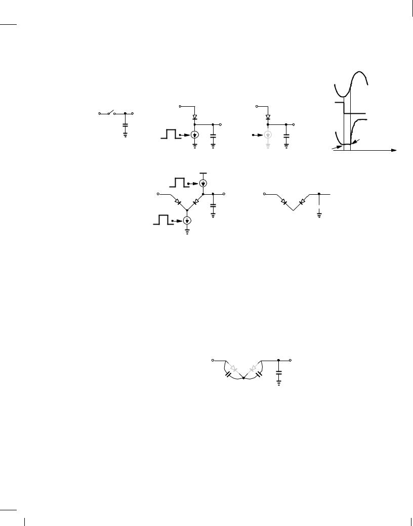
The level shift circuit of Fig. 3.59(b) can be transformed to an electronic switch. For example, many applications employ the topology shown in Fig. 3.61(a) to “sample” Vin across C1 and “freeze” the value when S1 turns off. Let us replace S1 with the level shift circuit and allow I1 to be turned on and off [Fig. 3.61(b)]. If I1 is on, Vout tracks Vin except for a level shift equal to VD;on. When I1 turns off, so does D1, evidently disconnecting C1 from the input and freezing the voltage across C1.
We used the term “evidently” in the last sentence because the circuit's true behavior somewhat differs from the above description. The assumption that D1 turns off holds only if C1 draws no current from D1, i.e., only if Vin,Vout remains less than VD;on. Now consider the case illustrated in Fig. 3.61(c), where I1 turns off at t = t1, allowing C1 to store a value equal to Vin1 , VD;on. As the input waveform completes a negative excursion and exceeds Vin1 at t = t2, the diode is forward-biased again, charging C1 with the input (in a manner similar to a peak detector). That is, even though I1 is off, D1 turns on for part of the cycle.
To resolve this issue, the circuit is modified as shown in Fig. 3.61(d), where D2 is inserted between D1 and C1, and I2 provides a bias current for D2. With both I1 and I2 on, the diodes operate in forward bias, VX = Vin , VD1, and Vout = VX + VD2 = Vin if VD1 = VD2. Thus, Vout tracks Vin with no level shift. When I1 and I2 turn off, the circuit reduces to that in Fig. 3.61(e), where the back-to-back diodes fail to conduct for any value of Vin , Vout, thereby isolating C1 from the input. In other words, the two diodes and the two current sources form an electronic switch.
BR |
Wiley/Razavi/Fundamentals of Microelectronics [Razavi.cls v. 2006] |
June 30, 2007 at 13:42 |
112 (1) |
|
|
|
|
112 |
Chap. 3 |
Diode Models and Circuits |
Vin |
Vout |
Vin |
|
Vin |
D1 |
|
D1 |
||
|
|
|
||
|
C1 |
|
Vout |
|
|
CK |
|
I 1 C1 |
I 1 |
|
(a) |
|
(b) |
|
|
|
|
VCC |
|
|
|
CK |
I 1 |
|
|
Vin |
|
Vout |
Vin |
|
|
|
C1 |
|
|
CK |
|
I 1 |
|
(d)
|
Vin |
|
|
CK |
|
Vout |
Vout |
|
C1 |
|
D1 turns on. |
|
|
|
D1 turns off. |
|
|
|
t 1 t 2 |
t |
(c)
 Vout
Vout
 C1
C1
(e)
Figure 3.61 (a) Switched-capacitor circuit, (b) realization of (a) using a diode as a switch, (c) problem of diode conduction, (d) more complete circuit, (e) equivalent circuit when I1 and I2 are off.
Example 3.38
Recall from Chapter 2 that diodes exhibit a junction capacitance in reverse bias. Study the effect of this capacitance on the operation of the above circuit.
Solution
Figure 3.62 shows the equivalent circuit for the case where the diodes are off, suggesting that the conduction of the input through the junction capacitances disturbs the output. Specifically, invoking the capacitive divider of Fig. 3.54(b) and assuming Cj1 = Cj2 = Cj , we have
Vin |
Vout |
Cj1 |
C1 |
Cj2 |
Figure 3.62 Feedthrough in the diode switch.
Vout = |
Cj =2 |
Vin: |
(3.116) |
Cj=2 + C1 |
To ensure this “feedthrough” is small, C1 must be sufficiently large.
Exercise
Calculate the change in the voltage at the left plate of Cj1 (with respect to ground) in terms of

BR |
Wiley/Razavi/Fundamentals of Microelectronics [Razavi.cls v. 2006] |
June 30, 2007 at 13:42 |
113 (1) |
|
|
|
|
Sec. 3.6 |
Chapter Summary |
113 |
Vin.
3.6 Chapter Summary
Silicon contains four atoms in its last orbital. It also contains a small number of free electrons at room temperature.
When an electron is freed from a covalent bond, a “hole” is left behind.
The bandgap energy is the minimum energy required to dislodge an electron from its covalent bond.
To increase the number of free carriers, semiconductors are “doped” with certain impurities. For example, addition of phosphorus to silicon increases the number of free electrons because phosphorus contains five electrons in its last orbital.
For doped or undoped semiconductors, np = n2. For example, in an n-type material, n ND
i
and hence p n2=ND .
i
Charge carriers move in semiconductors via two mechanisms: drift and diffusion.
The drift current density is proportional to the electric field and the mobility of the carriers and is given by Jtot = q( nn + pp)E.
The diffusion current density is proportional to the gradient of the carrier concentration and given by Jtot = q(Dndn=dx , Dpdp=dx).
A pn junction is a piece of semiconductor that receives n-type doping in one section and p-type doping in an adjacent section.
The pn junction can be considered in three modes: equilibrium, reverse bias, and forward bias.
Upon formation of the pn junction, sharp gradients of carrier densities across the junction result in a high current of electrons and holes. As the carriers cross, they leave ionized atoms behind, and a “depletion region” is formed. The electric field created in the depletion region eventually stops the current flow. This condition is called equilibrium.
The electric field in the depletion results in a built-in potential across the region equal to
kT=q) ln(NAND)=n2, typically in the range of 700 to 800 mV.
i
Under reverse bias, the junction carries negligible current and operates as a capacitor. The capacitance itself is a function of the voltage applied across the device.
Under forward bias, the junction carries a current that is an exponential function of the applied voltage: IS[exp(VF =VT ) , 1].
Since the exponential model often makes the analysis of circuits difficult, a constant-voltage model may be used in some cases to estimate the circuit's response with less mathematical labor.
Under a high reverse bias voltage, pn junctions break down, conducting a very high current. Depending on the structure and doping levels of the device, “Zener” or “avalanche” breakdown may occur.
Problems
In the following problems, assume VD;on = 800 mV for the constant-voltage diode model.
1. Plot the I/V characteristic of the circuit shown in Fig. 3.63.
BR |
Wiley/Razavi/Fundamentals of Microelectronics [Razavi.cls v. 2006] |
June 30, 2007 at 13:42 |
114 (1) |
|
|
|
|
114 |
|
Chap. 3 |
Diode Models and Circuits |
|
|
|
I X |
|
|
|
VX |
|
R1 |
|
|
D1 |
Ideal |
|
|
|
|
|
||
Figure 3.63
2.If the input in Fig. 3.63 is expressed as VX = V0 cos !t, plot the current flowing through the circuit as a function of time.
3. Plot IX as a function of VX for the circuit shown in Fig. 3.64 for two cases: VB = ,1 V and
I X
R1
D1 Ideal
VX
VB
Figure 3.64
VB = +1 V.
4.If in Fig. 3.64, VX = V0 cos !t, plot IX as a function of time for two cases: VB = ,1 V and
VB = +1 V.
5. For the circuit depicted in Fig. 3.65, plot IX as a function of VX for two cases: VB = ,1 V
|
I X |
|
|
VX |
D1 Ideal |
R |
1 |
|
|
||
|
|
VB |
|
Figure 3.65 |
|
|
|
and VB = +1 V.
6. Plot IX and ID1 as a function of VX for the circuit shown in Fig. 3.66. Assume VB > 0.
I X
R1
VX
 VB D1 Ideal
I D1
Figure 3.66
7.For the circuit depicted in Fig. 3.67, plot IX and IR1 as a function of VX for two cases: VB = ,1 V and VB = +1 V.
8.In the circuit of Fig. 3.68, plot IX and IR1 as a function of VX for two cases: VB = ,1 V and VB = +1 V.
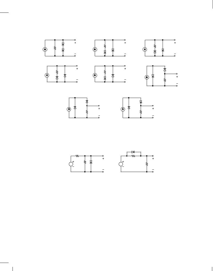
9.Plot the input/output characteristics of the circuits depicted in Fig. 3.69 using an ideal model for the diodes. Assume VB = 2 V.
BR |
Wiley/Razavi/Fundamentals of Microelectronics [Razavi.cls v. 2006] |
June 30, 2007 at 13:42 |
115 (1) |
|
|
|
|
Sec. 3.6 |
Chapter Summary |
|
I X |
|
|
|
|
|
115 |
|
|
|
|
|
|
|
|
|
|
|
|
|
|
|
|
|
|
|
R2 |
|
|
|
|
|
|
|
I R1 |
R1 D1 |
Ideal |
|
|
|
|
|
|
|
|
VX |
|
|
|
|
|
|
|
|
|
|
|
|
VB |
|
|
|
|
Figure 3.67 |
|
|
|
I X |
|
|
|
|
|
|
|
|
|
|
|
|
|
|
|
|
|
|
|
|
|
|
|
|
R2 |
|
|
|
|
|
|
|
I R1 |
|
R1 |
VB |
|
|
|
|
|
|
|
VX |
|
|
|
|
|
|
|
|
|
|
|
D1 |
Ideal |
|
|
|
|
Figure 3.68 |
|
|
|
|
|
|
|
|
|
|
|
R1 |
|
|
D1 |
VB |
|
|
VB |
|
|
|
|
|
|
|
|
|
|
|||
|
|
|
|
|
|
|
|
|
|
|
|
D1 |
|
|
|
|
|
|
R |
1 |
|
Vin |
Vout |
|
Vin |
R |
1 |
Vout |
Vin |
|
Vout |
|
|
|
D1 |
||||||||
|
VB |
|
|
|
|
|
|
|||
|
|
|
|
|
|
|
|
|
|
|
|
(a) |
|
|
(b) |
|
|
(c) |
|
||
|
|
D1 |
|
|
|
|
|
VB |
|
|
|
|
|
|
|
|
|
|
R1 |
|
|
|
Vin |
R |
1 |
Vout |
|
|
Vin |
D1 Vout |
|
|
|
|
|
|
|
|
|
||||
|
|
VB |
|
|
|
|
|
|
||
|
|
(d) |
|
|
|
|
|
(e) |
|
|
Figure 3.69
10.Repeat Problem 9 with a constant-voltage diode model.
11.If the input is given by Vin = V0 cos !t, plot the output of each circuit in Fig. 9 as function of time. Assume an ideal diode model.
12.Plot the input/output characteristics of the circuits shown in Fig. 3.70 using an ideal model for the diodes.
13.Repeat Problem 12 with a constant-voltage diode model.
14.Assuming the input is expressed as Vin = V0 cos !t, plot the output of each circuit in Fig. 3.70 as a function of time. Use an ideal diode model.
15.Assuming a constant-voltage diode model, plot Vout as a function of Iin for the circuits shown in Fig. 3.71.
16.In the circuits of Fig. 3.71, plot the current flowing through R1 as a function of Vin. Assume a constant-voltage diode model.
17.For the circuits illustrated in Fig. 3.71, plot Vout as a function of time if Iin = I0 cos !t. Assume a constant-voltage model and a relatively large I0.
18.Plot Vout as a function of Iin for the circuits shown in Fig. 3.72. Assume a constant-voltage diode model.
BR |
Wiley/Razavi/Fundamentals of Microelectronics [Razavi.cls v. 2006] |
June 30, 2007 at 13:42 |
116 (1) |
|
|
|
|
116 |
|
|
|
|
Chap. 3 |
Diode Models and Circuits |
|
|
VB |
|
|
R1 |
|
|
VB |
|
R1 |
|
|
|
|
|
D1 |
Vin |
D1 Vout |
|
Vin |
D1 |
Vout |
Vin |
R 1 Vout |
|
VB |
||||||
|
|
|
|
|
|
|
|
|
(a) |
|
|
(b) |
|
|
(c) |
|
VB |
|
|
|
D1 |
|
|
|
R |
1 |
Vout |
Vin |
R1 |
Vout |
|
|
Vin |
|
VB |
|
|||
|
D1 |
|
|
|
|
||
|
(d) |
|
|
(e) |
|
|
|
Figure 3.70
I in |
R |
1 |
D |
1 |
V |
I in |
R |
1 |
D1 |
|
|
|
out |
|
Vout |
||||
|
|
|
|
|
|
|
|
|
VB |
|
(a) |
|
|
|
(b) |
I in |
R |
1 |
Vout |
I in |
VB |
D1 |
|
V |
|||
|
VB |
|
D1 |
out |
|
|
|
R1 |
|||
|
|
|
|
||
|
(c) |
|
|
|
(d |
Figure 3.71
I |
R |
|
D1 |
1 |
V |
||
|
in |
|
out |
|
|
|
VB |
I in |
R |
1 |
Vout |
I in |
VB |
D1 |
|
V |
|||
|
VB |
|
D1 |
out |
|
|
|
R1 |
|||
|
|
|
|
||
(a) |
(b) |
(c) |
Figure 3.72
19.Plot the current flowing through R1 in the circuits of Fig. 3.72 as a function of Iin. Assume a constant-voltage diode model.
20. In the circuits depicted in Fig. 3.72, assume Iin = I0 cos !t, where I0 is relatively large. Plot Vout as a function of time using a constant-voltage diode model.
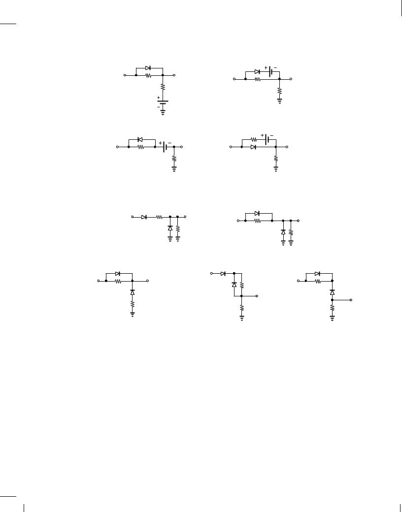
21.For the circuits shown in Fig. 3.73, plot Vout as a function of Iin assuming a constant-voltage model for the diodes.
22.Plot the current flowing through R1 as a function of Iin for the circuits of Fig. 3.73. Assume a constant-voltage diode model.
23.Plot the input/output characteristic of the circuits illustrated in Fig. 3.74 assuming a constantvoltage model.
BR |
Wiley/Razavi/Fundamentals of Microelectronics [Razavi.cls v. 2006] |
June 30, 2007 at 13:42 |
117 (1) |
|
|
|
|
Sec. 3.6 |
Chapter Summary |
117 |
|
|
|
D1 |
R 1 |
|
|
|
R 1 |
|
|
R |
|
Vout |
|
Vout |
|
Vout |
||
I in |
1 |
I in |
D2 |
I in |
|
||||
|
D2 |
|
D1 |
D2 |
|||||
|
|
|
|
D1 |
|
|
|
|
|
|
|
|
(a) |
|
(b) |
|
|
(c) |
|
|
R 1 |
|
R 1 |
|
|
|
D1 |
|
|
|
Vout |
|
Vout |
|
|
|
|||
I in |
|
|
I in |
D2 |
|
D2 |
|
||
|
D1 |
D2 |
|
I in |
|
||||
|
|
|
D1 |
|
|
R 1 |
Vout |
||
|
|
|
|
|
|
|
|
||
|
|
|
(d) |
|
(e) |
|
|
(f) |
|
|
|
|
D1 |
|
|
|
D1 |
|
|
|
|
|
D2 |
|
I in |
|
D2 |
|
|
|
|
|
I in |
Vout |
|
R 1 |
Vout |
|
|
|
|
|
R 1 |
|
|
|
|||
|
|
|
|
(g) |
|
|
(h) |
|
|
Figure 3.73
|
|
|
|
|
D1 |
R1 |
|
|
|
|
|
R |
|
D1 |
|
|
R1 |
2 |
Vout |
Vin |
R 2 Vout |
||
Vin |
|
|
|||
|
(a) |
|
|
|
(b) |
Figure 3.74
24.Plot the currents flowing through R1 and D1 as a function of Vin for the circuits of Fig. 3.74. Assume constant-voltage diode model.
25.Plot the input/output characteristic of the circuits illustrated in Fig. 3.75 assuming a constantvoltage model.
26.Plot the currents flowing through R1 and D1 as a function of Vin for the circuits of Fig. 3.75. Assume constant-voltage diode model.
27.Plot the input/output characteristic of the circuits illustrated in Fig. 3.76 assuming a constantvoltage model.
28.Plot the currents flowing through R1 and D1 as a function of Vin for the circuits of Fig. 3.76. Assume constant-voltage diode model.
29.Plot the input/output characteristic of the circuits illustrated in Fig. 3.77 assuming a constantvoltage model and VB = 2 V.
BR |
Wiley/Razavi/Fundamentals of Microelectronics [Razavi.cls v. 2006] |
June 30, 2007 at 13:42 |
118 (1) |
|
|
|
|
118 |
|
|
|
|
|
|
Chap. 3 Diode Models and Circuits |
||||
|
D1 |
|
|
|
|
D1 |
V |
B |
|
|
|
|
|
|
|
|
|
|
|
|
|
||
Vin |
R1 |
|
Vout |
Vin |
|
|
|
|
Vout |
|
|
|
|
|
|
R1 |
|
|
|
||||
|
|
R |
2 |
|
|
|
|
|
R2 |
|
|
|
|
|
|
|
|
|
|
|
|
||
|
|
|
|
|
|
|
|
|
|
|
|
|
|
VB |
|
|
|
|
|
|
|
|
|
|
(a) |
|
|
|
|
|
(b) |
|
|
|
|
|
D1 |
VB |
|
|
|
|
R1 |
VB |
|
|
|
|
|
|
|
|
|
|
|
|
|
|
|
Vin |
R1 |
|
|
Vout |
Vin |
|
D1 |
|
|
Vout |
|
|
|
|
R2 |
|
|
|
|
R2 |
|
||
|
|
|
|
|
|
|
|
|
|
||
|
|
(c) |
|
|
|
|
(d) |
|
|
|
|
Figure 3.75 |
|
|
|
|
|
|
|
|
|
|
|
|
D1 |
R1 |
|
|
|
|
D1 |
|
|
|
|
Vin |
|
Vout |
|
|
|
|
|
|
|
||
|
|
|
Vin |
|
|
|
|
Vout |
|
||
|
|
D2 |
|
|
|
R1 |
|
|
|
||
|
|
|
R2 |
|
|
|
D2 |
R2 |
|
||
|
|
|
|
|
|
|
|
|
|
||
|
|
(a) |
|
|
|
(b) |
|
|
|
|
|
D1 |
|
|
|
|
D1 |
|
|
|
|
D1 |
|
Vin |
|
Vout |
|
|
Vin |
|
|
|
|
Vin |
|
|
|
|
D2 |
R |
|
|
|
|
|||
R1 |
|
|
|
|
1 |
|
|
R1 |
|
||
D2 |
|
|
|
|
|
|
|
D2 |
|||
|
|
|
|
|
|
Vout |
|
|
|||
|
|
|
|
|
|
|
|
|
Vout |
||
|
R2 |
|
|
|
|
|
|
|
|
|
|
|
|
|
|
|
R2 |
|
|
|
R2 |
||
|
|
|
|
|
|
|
|
|
|||
(c) |
|
|
|
|
(d) |
|
|
|
|
(e) |
|
Figure 3.76
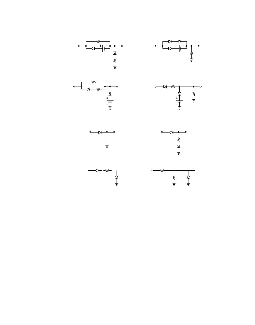
30.Plot the currents flowing through R1 and D1 as a function of Vin for the circuits of Fig. 3.77. Assume constant-voltage diode model.
31.Beginning with VD;on 800 mV for each diode, determine the change in Vout if Vin changes from +2:4 V to +2:5 V for the circuits shown in Fig. 3.78.
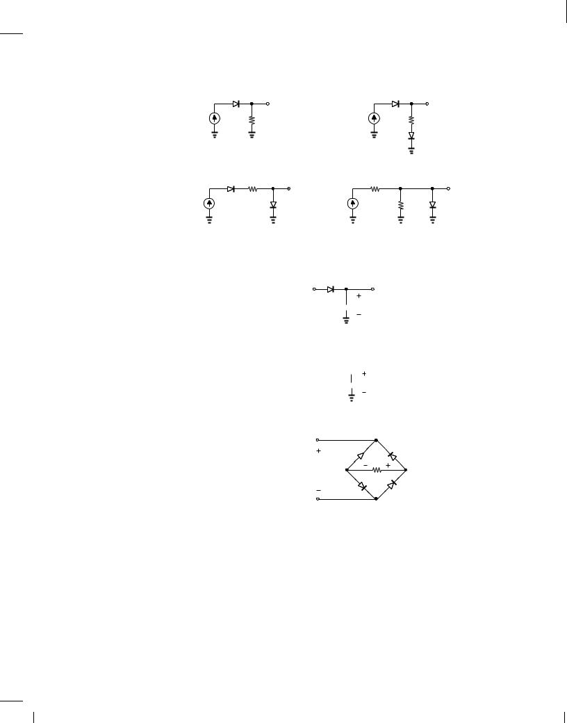
32.Beginning with VD;on 800 mV for each diode, calculate the change in Vout if Iin changes from 3 mA to 3.1 mA in the circuits of Fig. 3.79.
33.In Problem 32, determine the change in the current flowing through the 1-k resistor in each circuit.
34.Assuming Vin = Vp sin !t, plot the output waveform of the circuit depicted in Fig. 3.80 for an initial condition of +0:5 V across C1. Assume Vp = 5 V.
35.Repeat Problem 34 for the circuit shown in Fig. 3.81.
36.Suppose the rectifier of Fig. 3.32 drives a 100load with a peak voltage of 3.5 V. For a 1000- F smoothing capacitor, calculate the ripple amplitude if the frequency is 60 Hz.
BR |
Wiley/Razavi/Fundamentals of Microelectronics [Razavi.cls v. 2006] |
June 30, 2007 at 13:42 |
119 (1) |
|
|
|
|
Sec. 3.6 Chapter Summary
R1 |
|
|
|
Vin |
|
|
Vout |
D1 |
VB |
D |
2 |
|
|
||
|
|
R2 |
|
(a) |
|
|
|
R1 |
|
|
|
Vin |
|
Vout |
|
D1 R2 |
D2 |
|
|
|
|
VB |
|
(c) |
|
|
|
Figure 3.77 |
|
|
|
Vin |
D1 |
Vout |
|
|
|||
 R1 = 1 kΩ
(a)
D1 R1
Vin


 Vout
Vout
1 k Ω
D2
(c)
Figure 3.78
119
D1 |
R1 |
|
|
Vin |
|
|
Vout |
D1 |
V |
B |
R2 |
|
|
|
|
(b) |
|
|
|
D1 R1 |
|
|
|
Vin |
|
|
Vout |
|
|
D2 |
R2 |
|
|
VB |
|
(d) |
|
|
|
D1 |
|
|
|
Vin |
|
|
Vout |
|
|
R1 = 1 kΩ |
|
|
|
D2 |
|
(b) |
|
|
|
R1 |
|
|
|
Vin |
|
|
Vout |
1 k Ω |
2 k Ω |
D2 |
|
R 2 |
|||
(d)
37.A 3-V adaptor using a half-wave rectifier must supply a current of 0.5 A with a maximum ripple of 300 mV. For a frequency of 60 Hz, compute the minimum required smoothing capacitor.
38.Assume the input and output grounds in a full-wave rectifier are shorted together. Draw the output waveform with and without the load capacitor and explain why the circuit does not operate as a rectifier.
39.Plot the voltage across each diode in Fig. 3.38(b) as a function of time if Vin = V0 cos !t. Assume a constant-voltage diode model and VD > VD;on.
40.While constructing a full-wave rectifier, a student mistakenly has swapped the terminals of D3 as depicted in Fig. 3.82. Explain what happens.
41. A full-wave rectifier is driven by a sinusoidal input Vin = V0 cos !t, where V0 = 3 V and ! = 2 (60 Hz). Assuming VD;on = 800 mV, determine the ripple amplitude with a 1000- F smoothing capacitor and a load resistance of 30 .
42.Suppose the negative terminals of Vin and Vout in Fig. 3.38(b) are shorted together. Plot the input-output characteristic assuming an ideal diode model and explaining why the circuit does not operate as a full-wave rectifier.
BR |
Wiley/Razavi/Fundamentals of Microelectronics [Razavi.cls v. 2006] |
June 30, 2007 at 13:42 |
120 (1) |
|
|
|
|
120 |
|
|
Chap. 3 Diode Models and Circuits |
||
D1 |
Vout |
|
|
D1 |
Vout |
|
|
|
|
||
I in |
R1 = 1 kΩ |
|
I in |
R1 |
= 1 kΩ |
|
|
|
|||
|
|
|
|
D2 |
|
|
(a) |
|
|
(b) |
|
D1 |
R1 |
|
|
R1 |
|
|
Vout |
|
|
1 k Ω |
Vout |
I in |
1 k Ω |
I in |
|
|
|
D2 |
|
R 2 2 k Ω |
D2 |
||
|
(c) |
|
|
(d) |
|
Figure 3.79 |
|
|
|
|
|
|
Vin |
D1 |
|
Vout |
|
|
|
|
|
||
C1  0.5 V
0.5 V
Figure 3.80
D1
Vin


 Vout
Vout
C1  0.5 V
0.5 V
Figure 3.81
D 2  D 3
D 3
Vout
Vin
RL
D 4 |
D 1 |
Figure 3.82
43.Suppose in Fig. 3.43, the diodes carry a current of 5 mA and the load, a current of 20 mA. If the load current increases to 21 mA, what is the change in the total voltage across the three diodes? Assume R1 is much greater than 3rd.
44.In this problem, we estimate the ripple seen by the load in Fig. 3.43 so as to appreciate the regulation provided by the diodes. For simplicity, neglect the load. Also, fin = 60 Hz,
C1 = 100 F, R1 = 1000 , and the peak voltage produced by the transformer is equal to 5 V.
(a)Assuming R1 carries a relatively constant current and VD;on 800 mV, estimate the ripple amplitude across C1.
(b)Using the small-signal model of the diodes, determine the ripple amplitude across the load.