

Fundamentals of Microelectronics
.pdfBR |
Wiley/Razavi/Fundamentals of Microelectronics [Razavi.cls v. 2006] |
June 30, 2007 at 13:42 |
11 (1) |
|
|
|
|
Sec. 1.3 Basic Concepts 11
realize the NOT and NOR functions shown in Fig. 1.15. Based on these implementations, we
NOT Gate |
|
|
NOR Gate |
|
A |
Y = A |
A |
Y = A + B |
|
B |
||||
|
|
|
||
Figure 1.15 NOT and NOR gates. |
|
|
|
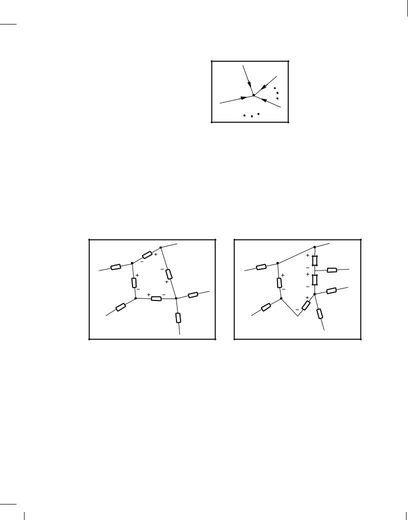
then determine various properties of each circuit. For example, what limits the speed of a gate? How much power does a gate consume while running at a certain speed? How robustly does a gate operate in the presence of nonidealities such as noise (Fig. 1.16)?
?
Figure 1.16 Response of a gate to a noisy input.
Example 1.4
Consider the circuit shown in Fig. 1.17, where switch S1 is controlled by the digital input. That
R L 
A |
VDD |
S 1 V |
|
|
out |
Figure 1.17
is, if A is high, S1 is on and vice versa. Prove that the circuit provides the NOT function.
Solution
If A is high, S1 is on, forcing Vout to zero. On the other hand, if A is low, S1 remains off, drawing no current from RL. As a result, the voltage drop across RL is zero and hence Vout = VDD; i.e., the output is high. We thus observe that, for both logical states at the input, the output assumes the opposite state.
Exercise
Determine the logical function if S1 and RL are swapped and Vout is sensed across RL.
The above example indicates that switches can perform logical operations. In fact, early digital circuits did employ mechanical switches (relays), but suffered from a very limited speed (a few kilohertz). It was only after “transistors” were invented and their ability to act as switches was recognized that digital circuits consisting of millions of gates and operating at high speeds (several gigahertz) became possible.
1.3.4 Basic Circuit Theorems
Of the numerous analysis techniques taught in circuit theory courses, some prove particularly important to our study of microelectronics. This section provides a review of such concepts.
BR |
Wiley/Razavi/Fundamentals of Microelectronics [Razavi.cls v. 2006] |
June 30, 2007 at 13:42 |
12 (1) |
|
|
|
|
12
Figure 1.18 Illustration of KCL.
Chap. 1 Introduction to Microelectronics
I 1 |
I n |
|
|
I 2 |
I j |
Kirchoff's Laws The Kirchoff Current Law (KCL) states that the sum of all currents flowing into a node is zero (Fig. 1.18):
XIj = 0: |
(1.5) |
j
KCL in fact results from conservation of charge: a nonzero sum would mean that either some of the charge flowing into node X vanishes or this node produces charge.
The Kirchoff Voltage Law (KVL) states that the sum of voltage drops around any closed loop in a circuit is zero [Fig. 1.19(a)]:
|
2 |
|
|
|
|
|
V2 |
|
|
V2 |
2 |
|
V3 |
3 |
|
|
|
|
|
V1 |
V3 |
3 |
|
1 |
V1 |
1 |
|||
|
V4 |
|
|
|
|
|
4 |
|
|
V4 |
|
|
|
|
|
4 |
|
|
|
|
|
|
|
|
(a) |
|
|
(b) |
|
Figure 1.19 (a) Illustration of KVL, (b) slightly different view of the circuit .
XVj = 0; |
(1.6) |
j
where Vj denotes the voltage drop across element number j. KVL arises from the conservation of the “electromotive force.” In the example illustrated in Fig. 1.19(a), we may sum the voltages in the loop to zero: V1 + V2 + V3 + V4 = 0. Alternatively, adopting the modified view shown in Fig. 1.19(b), we can say V1 is equal to the sum of the voltages across elements 2, 3, and 4: V1 = V2 +V3 +V4. Note that the polarities assigned to V2, V3, and V4 in Fig. 1.19(b) are different from those in Fig. 1.19(a).
In solving circuits, we may not know a priori the correct polarities of the currents and voltages. Nonetheless, we can simply assign arbitrary polarities, write KCLs and KVLs, and solve the equations to obtain the actual polarities and values.
BR |
Wiley/Razavi/Fundamentals of Microelectronics [Razavi.cls v. 2006] |
June 30, 2007 at 13:42 |
13 (1) |
|
|
|
|
Sec. 1.3 Basic Concepts 13
Example 1.5
The topology depicted in Fig. 1.20 represents the equivalent circuit of an amplifier. The dependent current source i1 is equal to a constant, gm,6 multiplied by the voltage drop across
v in |
r π vπ i 1 |
gm vπ R L |
v out |
v out |
|
R L |
|||||
|
|||||
|
|
|
|
Figure 1.20
r . Determine the voltage gain of the amplifier, vout=vin.
Solution
We must compute vout in terms of vin, i.e., we must eliminate v from the equations. Writing a KVL in the “input loop,” we have
vin = v ; |
(1.7) |
|
and hence gmv = gmvin. A KCL at the output node yields |
|
|
gmv + vout |
= 0: |
(1.8) |
RL |
|
|
It follows that |
|
|
vout = ,g |
R : |
(1.9) |
m |
L |
|
vin |
|
|
Note that the circuit amplifies the input if gmRL > 1. Unimportant in most cases, the negative sign simply means the circuit “inverts” the signal.
Exercise
Repeat the above example if r ! infty.
Example 1.6
Figure 1.21 shows another amplifier topology. Compute the gain.
r π vπ i 1 gm vπ R L |
v out |
v in
Figure 1.21
6What is the dimension of gm?
BR |
Wiley/Razavi/Fundamentals of Microelectronics [Razavi.cls v. 2006] |
June 30, 2007 at 13:42 |
14 (1) |
|
|
|
|
14 |
Chap. 1 |
Introduction to Microelectronics |
The KCL at the output node is similar to (1.8). Thus, |
|
|
|
vout = g R |
L |
: |
(1.11) |
m |
|
|
|
vin |
|
|
|
Interestingly, this type of amplifier does not invert the signal.
Exercise
Repeat the above example if r ! infty.
Example 1.7
A third amplifier topology is shown in Fig. 1.22. Determine the voltage gain.
|
|
|
|
|
|
|
|
|
|
|
|
|
|
|
|
|
|
|
|
|
|
|
|
|
|
|
|
|
|
|
|
|
|
|
|
|
gm vπ |
|
|
|
|
|
|
||
|
|
|
|
|
|
v in |
|
|
|
|
|
|
r π |
|
vπ i 1 |
|
|
|
|
|
|
|
|
|
|
|
|||||||||||||||||||
|
|
|
|
|
|
|
|
|
|
|
|
|
|
|
|
|
|
|
|
|
|
|
|
||||||||||||||||||||||
|
|
|
|
|
|
|
|
|
|
|
|
|
|
|
|
|
|
|
|
|
|
|
|
||||||||||||||||||||||
|
|
|
|
|
|
|
|
|
|
|
|
|
|
||||||||||||||||||||||||||||||||
|
|
|
|
|
|
|
|
|
|
|
|
|
|
|
|
|
|
|
|
|
|
|
|
|
|
|
|
|
|
|
|
|
|
|
|
|
|
|
|
|
|
|
|
|
|
|
|
|
|
|
|
|
|
|
|
|
|
|
|
|
|
|
|
|
|
|
|
|
|
|
|
|
|
|
|
|
|
|
|
|
|
|
|
|
|
|
|
|
|
|
|
Figure 1.22 |
|
|
|
|
|
|
|
|
|
|
|
|
|
|
|
|
|
|
|
|
R E |
|
|
v |
|
out |
|
|
|
|
|
|
|
||||||||||||
|
|
|
|
|
|
|
|
|
|
|
|
|
|
|
|
|
|
|
|
|
|
|
|
|
|
|
|
|
|
|
|
|
|
|
|
|
|
|
|
|
|
|
|
|
|
|
|
|
|
|
|
|
|
|
|
|
|
|
|
|
|
|
|
|
|
|
|
|
|
|
|
|
|
|
|
|
|
|
|
|
|
|
|
|
|
|
|
|
|
|
|
|
|
|
|
|
|
|
|
|
|
|
|
|
|
|
|
|
|
|
|
|
|
|
|
|
|
|
|
|
|
|
|
|
|
|
|
|
|
|
|
|
|
|
|
|
|
Solution |
|
|
|
|
|
|
|
|
|
|
|
|
|
|
|
|
|
|
|
|
|
|
|
|
|
|
|
|
|
|
|
|
|
|
|
|
|
|
|
|
|
|
|
|
|
We first write a KVL around the loop consisting of vin, r , and RE: |
|
||||||||||||||||||||||||||||||||||||||||||||
|
|
|
|
|
|
vin = v + vout: |
|
|
|
|
|
|
|
|
|
|
|
|
|
|
|
(1.12) |
|||||||||||||||||||||||
That is, v = vin , vout. Next, noting that the currents v =r and gmv flow |
into the output |
||||||||||||||||||||||||||||||||||||||||||||
node, and the current vout=RE flows |
out of it, we write a KCL: |
|
|
|
|
|
|
|
|
||||||||||||||||||||||||||||||||||||
|
|
|
|
|
|
v + g |
v |
= vout : |
|
|
|
|
|
|
|
|
|
|
|
|
|
|
|
(1.13) |
|||||||||||||||||||||
|
|
|
|
|
|
r |
m |
|
|
|
RE |
|
|
|
|
|
|
|
|
|
|
|
|
|
|
|
|
||||||||||||||||||
|
|
|
|
|
|
|
|
|
|
|
|
|
|
|
|
|
|
|
|
|
|
|
|
|
|
|
|
||||||||||||||||||
Substituting vin , vout for v gives |
|
|
|
|
|
|
|
|
|
|
|
|
|
|
|
|
|
|
|
|
|
|
|
|
|
|
|
|
|
|
|
|
|
|
|
|
|
|
|
|
|
||||
v |
|
|
1 |
+ g |
|
= v |
|
|
1 |
+ |
|
1 |
+ g |
|
; |
(1.14) |
|||||||||||||||||||||||||||||
|
|
|
|
|
|
|
|
||||||||||||||||||||||||||||||||||||||
|
in |
|
r |
|
m |
|
|
|
|
|
|
|
|
out |
|
|
RE |
r |
|
|
|
|
|
|
m |
|
|
|
|
|
|
|
|||||||||||||
and hence |
|
|
|
|
|
|
|
|
|
|
|
|
|
|
|
|
|
|
|
|
|
|
|
|
|
|
|
|
|
|
|
|
|
|
|
|
|
|
|
|
|
|
|
|
|
|
|
|
|
|
|
|
|
|
|
|
|
|
|
|
1 |
+ gm |
|
|
|
|
|
|
|
|
|
|
|
|
|
|
|
|
|||||||||||||
|
|
|
vout |
|
|
|
|
|
|
|
|
|
|
|
|
|
|
|
|
|
|
|
|
|
|
|
|
|
|
|
|||||||||||||||
|
|
|
|
|
|
|
|
|
|
|
|
|
r |
|
|
|
|
|
|
|
|
|
|
|
|
|
|
|
(1.15) |
||||||||||||||||
|
|
|
|
vin |
|
= |
|
1 |
|
|
|
|
1 |
|
|
|
|
|
|
|
|
|
|
|
|
|
|
|
|
|
|
|
|
|
|
|
|
|
|
||||||
|
|
|
|
|
|
|
|
|
RE |
+ r |
+ gm |
|
|
|
|
|
|
|
|
|
|
|
|
|
|
|
|
||||||||||||||||||
BR |
Wiley/Razavi/Fundamentals of Microelectronics [Razavi.cls v. 2006] |
June 30, 2007 at 13:42 |
15 (1) |
|
|
|
|
Sec. 1.3 Basic Concepts |
|
|
15 |
|
(1 |
+ gmr )RE |
|
(1.16) |
|
= |
|
|
: |
|
r + |
(1 + gmr )RE |
|||
Note that the voltage gain always remains below unity. Would such an amplifier prove useful at all? In fact, this topology exhibits some important properties that make it a versatile building block.
Exercise
Repeat the above example if r ! infty.
The above three examples relate to three amplifier topologies that are studied extensively in Chapter 5.
Thevenin and Norton Equivalents While Kirchoff's laws can always be utilized to solve any circuit, the Thevenin and Norton theorems can both simplify the algebra and, more importantly, provide additional insight into the operation of a circuit.
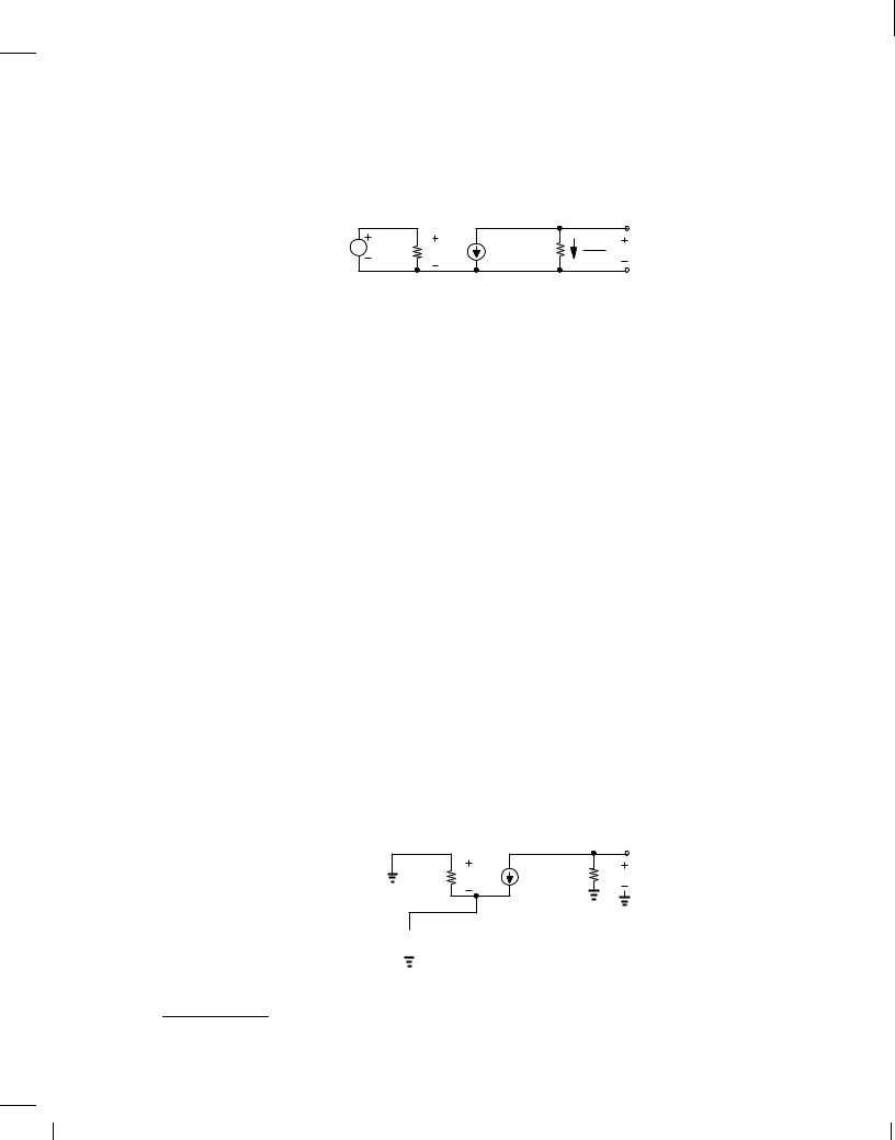
Thevenin's theorem states that a (linear) one-port network can be replaced with an equivalent circuit consisting of one voltage source in series with one impedance. Illustrated in Fig. 1.23(a), the term “port” refers to any two nodes whose voltage difference is of interest. The equivalent
Vj
iX
Port j
v
X
Z |
Thev |
v Thev
Z
Thev
(a) |
(b) |
Figure 1.23 (a) Thevenin equivalent circuit, (b) computation of equivalent impedance.
voltage, vT hev, is obtained by leaving the port open and computing the voltage created by the actual circuit at this port. The equivalent impedance, ZT hev, is determined by setting all independent voltage and current sources in the circuit to zero and calculating the impedance between the two nodes. We also call ZT hev the impedance “seen” when “looking” into the output port [Fig.
1.23(b)]. The impedance is computed by applying a voltage source across the port and obtaining the resulting current. A few examples illustrate these principles.
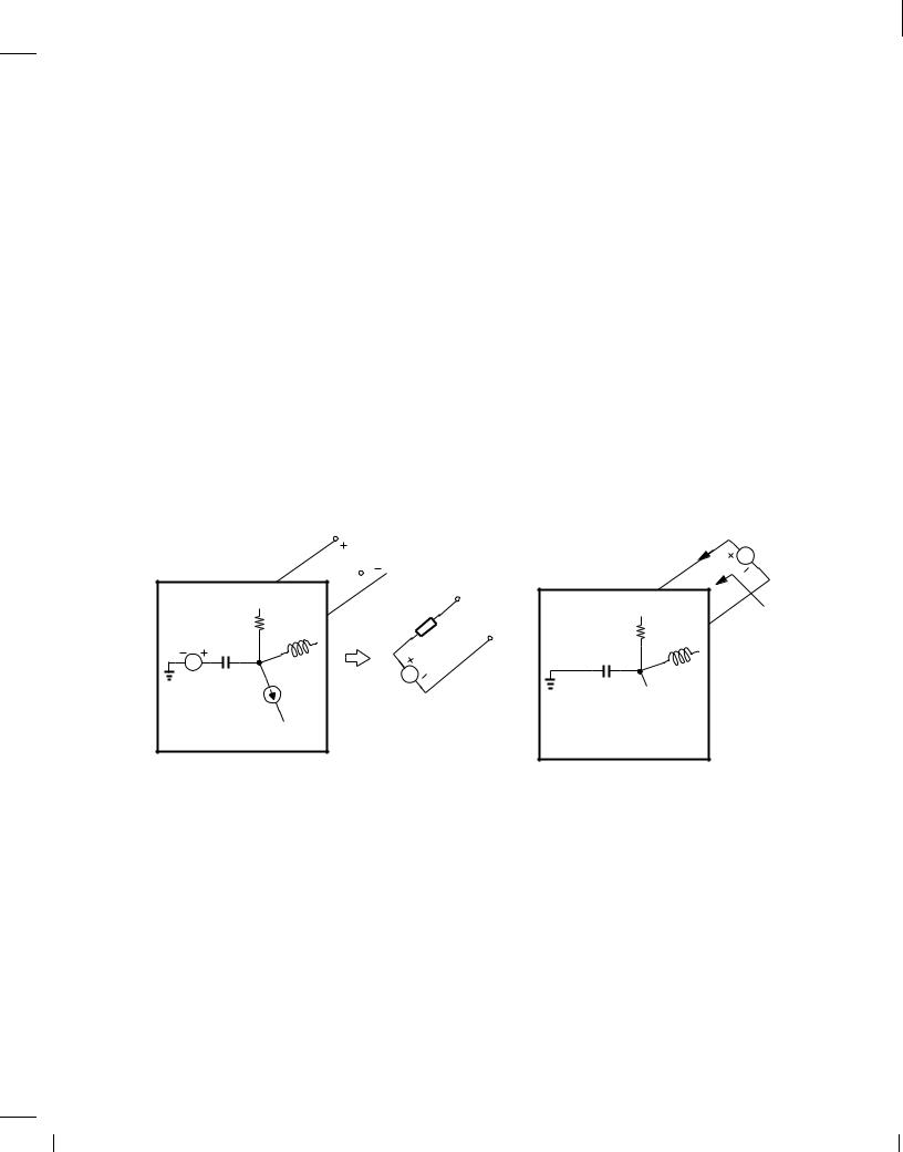
Example 1.8
Suppose the input voltage source and the amplifier shown in Fig. 1.20 are placed in a box and only the output port is of interest [Fig. 1.24(a)]. Determine the Thevenin equivalent of the circuit.
Solution
We must compute the open-circuit output voltage and the impedance seen when looking into the
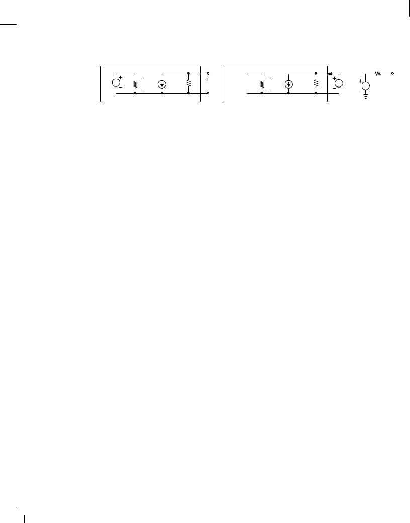
BR |
Wiley/Razavi/Fundamentals of Microelectronics [Razavi.cls v. 2006] |
June 30, 2007 at 13:42 |
16 (1) |
|
|
|
|
16 |
Chap. 1 |
Introduction to Microelectronics |
|
|
|
|
|
|
|
|
|
|
|
|
|
|
|
|
|
|
|
|
|
|
|
i X |
RL |
|
|
v in |
|
π |
|
π |
|
1 |
g |
m |
π |
R L |
v out |
v in = 0 |
|
π |
|
π |
|
1 |
g |
m |
π |
R L |
v X |
m |
L |
in |
r |
|
v |
|
i |
|
v |
|
r |
|
v |
|
i |
|
v |
|
− g |
R v |
|
(a) |
(b) |
(c) |
Figure 1.24
output port. The Thevenin voltage is obtained from Fig. 1.24(a) and Eq. (1.9):
vT hev = vout |
(1.17) |
= ,gmRLvin: |
(1.18) |
To calculate ZT hev, we set vin to zero, apply a voltage source, vX , across the output port, and determine the current drawn from the voltage source, iX. As shown in Fig. 1.24(b), setting vin to zero means replacing it with a short circuit. Also, note that the current source gmv remains in the circuit because it depends on the voltage across r , whose value is not known a priori.
How do we solve the circuit of Fig. 1.24(b)? We must again eliminate v . Fortunately, since both terminals of r are tied to ground, v = 0 and gmv = 0. The circuit thus reduces to RL and
iX = vX : |
(1.19) |
RL |
|
That is, |
|
RT hev = RL: |
(1.20) |
Figure 1.24(c) depicts the Thevenin equivalent of the input voltage source and the amplifier. In this case, we call RT hev (= RL) the “output impedance” of the circuit.
Exercise
Repeat the above example if r ! 1.
With the Thevenin equivalent of a circuit available, we can readily analyze its behavior in the presence of a subsequent stage or “load.”
Example 1.9
The amplifier of Fig. 1.20 must drive a speaker having an impedance of Rsp. Determine the voltage delivered to the speaker.
Solution
Shown in Fig. 1.25(a) is the overall circuit arrangement that must solve. Replacing the section in the dashed box with its Thevenin equivalent from Fig. 1.24(c), we greatly simplify the circuit [Fig. 1.25(b)], and write
vout = ,gmRLvin |
Rsp |
(1.21) |
Rsp + RL |
||
= ,gmvin(RLjjRsp): |
(1.22) |
|
BR |
Wiley/Razavi/Fundamentals of Microelectronics [Razavi.cls v. 2006] |
June 30, 2007 at 13:42 |
17 (1) |
|
|
|
|
Sec. 1.3 |
Basic Concepts |
|
|
|
|
|
|
|
|
|
|
17 |
|||||
|
|
|
|
|
|
|
|
|
|
|
|
|
|
|
|
RL |
|
v in |
r |
π |
v |
π |
i |
1 |
g |
m |
v |
π |
R L |
v out |
Rsp |
− g |
R v |
v out |
Rsp |
|
|
|
|
|
|
|
|
|
m |
L |
in |
|
|||||
(a) |
(b) |
Figure 1.25
Exercise
Repeat the above example if r ! 1.
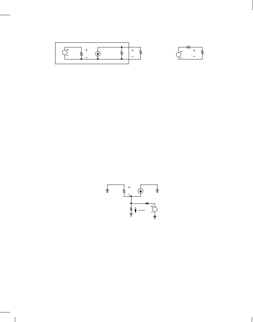
Example 1.10
Determine the Thevenin equivalent of the circuit shown in Fig. 1.22 if the output port is of interest.
Solution
The open-circuit output voltage is simply obtained from (1.16):
(1 |
+ gmr )RL |
(1.23) |
||
vT hev = |
|
|
vin: |
|
r + |
(1 + gmr )RL |
|||
To calculate the Thevenin impedance, we set vin to zero and apply a voltage source across the output port as depicted in Fig. 1.26. To eliminate v , we recognize that the two terminals of r
r π vπ i 1 |
gm vπ |
|
|
|
i X |
|
|
R L |
v X |
v X |
|
R L |
|||
|
|
Figure 1.26
are tied to those of vX and hence
v = ,vX : |
(1.24) |
We now write a KCL at the output node. The currents v =r , gmv , and iX flow and the current vX =RL flows out of it. Consequently,
v + g |
v |
|
+ i = vX |
; |
|
r |
m |
X |
RL |
|
|
|
|
|
|
||
or
into this node
(1.25)
|
1 |
+ g |
m |
(,v |
X |
) + i = |
vX |
: |
(1.26) |
|
|
||||||||
|
r |
|
X |
RL |
|
|
|||
|
|
|
|
|
|
|
|||
BR |
Wiley/Razavi/Fundamentals of Microelectronics [Razavi.cls v. 2006] |
June 30, 2007 at 13:42 |
18 (1) |
|
|
|
|
18 Chap. 1 Introduction to Microelectronics
That is, |
|
|
|
|
R |
= vX |
|
(1.27) |
|
T hev |
|
iX |
|
|
|
|
|
|
|
|
= |
r RL |
: |
(1.28) |
|
r + (1 + gmr )RL |
|||
Exercise
What happens if RL = 1?
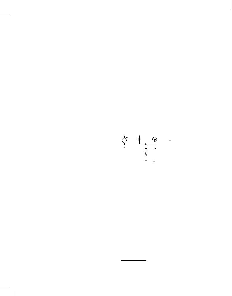
Norton's theorem states that a (linear) one-port network can be represented by one current source in parallel with one impedance (Fig. 1.27). The equivalent current, iNor, is obtained by
Port j
Z
Nor
i
Nor
Figure 1.27 Norton's theorem.
shorting the port of interest and computing the current that flows through it. The equivalent impedance, ZNor, is determined by setting all independent voltage and current sources in the circuit to zero and calculating the impedance seen at the port. Of course, ZNor = ZT hev.
Example 1.11
Determine the Norton equivalent of the circuit shown in Fig. 1.20 if the output port is of interest.
Solution
As depicted in Fig. 1.28(a), we short the output port and seek the value of iNor. Since the voltage
|
|
|
|
|
i Nor |
|
|
|
v in |
r π |
vπ |
i 1 |
gm vπ R L |
Short |
gmvin |
R L |
|
Circuit |
||||||||
|
||||||||
|
|
|
|
(a) |
|
|
(b) |
Figure 1.28
across RL is now forced to zero, this resistor carries no current. A KCL at the output node thus yields
iNor = ,gmv |
(1.29) |
BR |
Wiley/Razavi/Fundamentals of Microelectronics [Razavi.cls v. 2006] |
June 30, 2007 at 13:42 |
19 (1) |
|
|
|
|
Sec. 1.4 |
Chapter Summary |
19 |
|
= ,gmvin: |
(1.30) |
Also, from Example 1.8, RNor (= RT hev) = RL. The Norton equivalent therefore emerges as shown in Fig. 1.28(b). To check the validity of this model, we observe that the flow of iNor through RL produces a voltage of ,gmRLvin, the same as the output voltage of the original circuit.
Exercise
Repeat the above example if a resistor of value R1 is added between the top terminal of vin and the output node.
Example 1.12
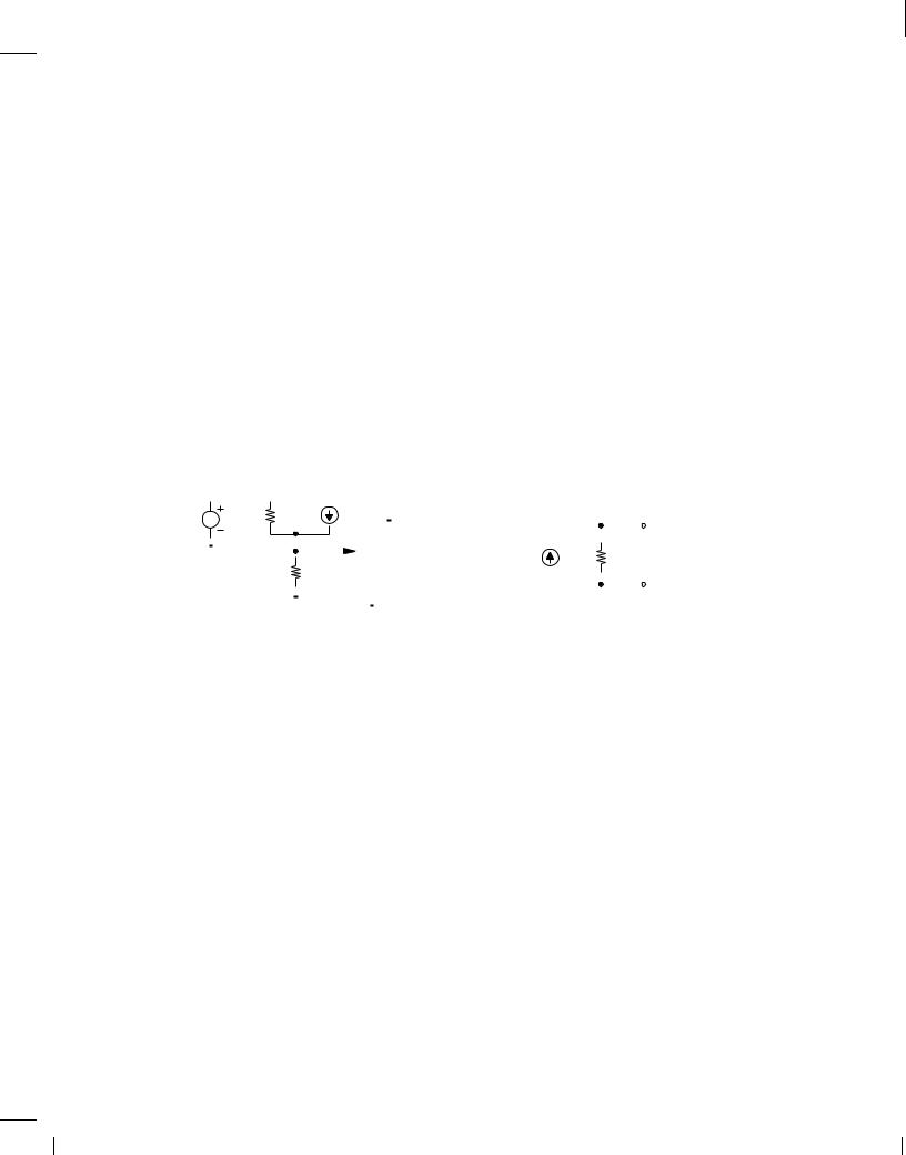
Determine the Norton equivalent of the circuit shown in Fig. 1.22 if the output port is interest.
Solution
Shorting the output port as illustrated in Fig. 1.29(a), we note that RL carries no current. Thus,
|
|
|
|
|
|
|
|
|
|
|
|
|
|
|
|
gm vπ |
|
|
|
|
|
|
|
|
|
|
|
|
|
|
|
|
|
|
|
|
|
|||||
v in |
|
|
|
r π |
vπ i 1 |
|
|
|
|
|
|
( |
1 |
|
+ |
g |
)v |
|
|
|
|
r π R L |
||||||||||||||||||||
|
|
|
|
|
|
|
|
|
|
|
|
|
|
|||||||||||||||||||||||||||||
|
|
|
|
|
|
|
|
|
|
|
|
|
|
|||||||||||||||||||||||||||||
|
|
|
|
|
|
|
|
|
|
|
|
|
|
|
|
|
|
|
|
|
|
|
|
|
|
|
|
|
|
|
|
|
||||||||||
|
|
|
|
|
|
|
|
|
|
|
|
|
|
|
|
|
|
|
|
|
|
|
|
|
|
|
|
|
|
|
|
|
||||||||||
|
|
|
|
|
|
|
|
|
|
|
|
|
|
|
|
|
|
|
|
|
|
|
|
|
|
|
|
|
|
|||||||||||||
|
|
|
|
|
|
|
|
|
|
|
|
|
|
|
|
|
|
|
|
|
|
|
|
|
|
|
|
|
|
|
|
|
|
|
|
|||||||
|
|
|
|
|
|
R |
|
|
|
|
|
|
|
|
i Nor |
|
|
|
|
|
|
|
|
|
|
|
r π |
|
m |
|
in |
|
|
r π + (1+ gmr π ) R L |
||||||||
|
|
|
|
|
|
L |
|
|
|
|
|
|
|
|
|
|
|
|
|
|||||||||||||||||||||||
|
|
|
|
|
|
|
|
|
|
|
|
|
|
|
|
|
|
|
|
|
|
|
|
|
|
|
|
|
|
|
|
|
|
|
||||||||
|
|
|
|
|
|
|
|
|
|
|
|
|
|
|
|
|
|
|
|
|
|
|
|
|
|
|
|
|
|
|
|
|
|
|
|
|
|
|
|
|
|
|
|
|
|
|
|
|
|
|
|
|
|
|
|
|
|
|
|
|
|
|
|
|
|
|
|
|
|
|
|
|
|
|
|
|
|
|
|
|
|
|
|
||
|
|
|
|
|
|
|
|
|
|
|
|
|
|
|
|
|
|
|
|
|
|
|
|
|
|
|
|
|
|
|
|
|
|
|
|
|
|
|
|
|||
|
|
|
|
|
|
|
|
|
|
|
|
|
(a) |
|
|
|
|
|
|
|
|
|
|
|
|
|
|
|
|
|
|
|
|
|
|
(b) |
||||||
|
|
|
|
|
|
|
|
|
|
|
|
|
|
|
|
|
|
|
|
|
|
|
|
|
|
|
|
|
|
|
|
|
|
|
||||||||
|
|
|
|
|
|
|
|
|
|
|
|
|
|
|
|
|
|
|
|
|
|
|
|
|
|
|
|
|
|
|
|
|
|
|
||||||||
Figure 1.29 |
|
|
|
|
|
|
|
|
|
|
|
|
|
|
|
|
|
|
|
|
|
|
|
|
|
|
|
|
|
|
|
|
|
|
|
|
|
|||||
|
|
|
|
|
|
|
|
|
|
|
|
|
|
|
|
|
|
|
|
|
|
|
|
i |
Nor |
= v + g |
|
v |
|
: |
|
|
(1.31) |
|||||||||
|
|
|
|
|
|
|
|
|
|
|
|
|
|
|
|
|
|
|
|
|
|
|
|
|
|
|
r |
m |
|
|
|
|
|
|
|
|
|
|||||
|
|
|
|
|
|
|
|
|
|
|
|
|
|
|
|
|
|
|
|
|
|
|
|
|
|
|
|
|
|
|
|
|
|
|
|
|
|
|
|
|||
Also, vin = v (why?), yielding |
|
|
|
|
|
|
|
|
|
|
|
|
|
|
|
|
|
|||||||||||||||||||||||||
|
|
|
|
|
|
|
|
|
|
|
|
|
|
|
|
|
|
|
|
iNor = |
1 |
+ gm vin: |
|
(1.32) |
||||||||||||||||||
|
|
|
|
|
|
|
|
|
|
|
|
|
|
|
|
|
|
|
|
|
|
|||||||||||||||||||||
|
|
|
|
|
|
|
|
|
|
|
|
|
|
|
|
|
|
|
|
|
|
|
|
|
|
|
|
r |
|
|
|
|
|
|
|
|
|
|
|
|
||
With the aid of RT hev found in Example 1.10, we construct the Norton equivalent depicted in Fig. 1.29(b).
Exercise
What happens if r = infty?
1.4 Chapter Summary
Electronic functions appear in many devices, including cellphones, digital cameras, laptop computers, etc.

BR |
Wiley/Razavi/Fundamentals of Microelectronics [Razavi.cls v. 2006] |
June 30, 2007 at 13:42 |
20 (1) |
|
|
|
|
20 |
Chap. 1 |
Introduction to Microelectronics |
Amplification is an essential operation in many analog and digital systems.
Analog circuits process signals that can assume various values at any time. By contrast, digital circuits deal with signals having only two levels and switching between these values at known points in time.
Despite the “digital revolution,” analog circuits find wide application in most of today's electronic systems.
The voltage gain of an amplifier is defined as vout=vin and sometimes expressed in decibels (dB) as 20 log(vout=vin).
Kirchoff's current law (KCL) states that the sum of all currents flowing into any node is zero. Kirchoff's voltage law (KVL) states that the sum of all voltages around any loop is zero.
Norton's theorem allows simplifying a one-port circuit to a current source in parallel with an impedance. Similarly, Thevenin's theorem reduces a one-port circuit to a voltage source in series with an impedance.