

Fundamentals of Microelectronics
.pdfBR |
Wiley/Razavi/Fundamentals of Microelectronics [Razavi.cls v. 2006] |
June 30, 2007 at 13:42 |
241 (1) |
|
|
|
|
Sec. 5.3 |
Bipolar Amplifier Topologies |
241 |
Exercise
Does the circuit operate better if Vb is raised?
The above examples imply that the emitter can remain neither open nor shorted to ground, thereby requiring some bias element. Shown in Fig. 5.79(a) is an example, where RE provides a path for the bias current at the cost of lowering the input impedance. We recognize that Rin now consists of two parallel components: (1) 1=gm, seen looking “up” into the emitter (with the base at ac ground) and (2) RE, seen looking “down.” Thus,
|
VCC |
|
|
VCC |
|
R C |
|
|
R C |
|
v out |
|
|
v out |
1 |
Q 1 |
|
|
Q 1 |
g m |
|
Vb |
X |
Vb |
|
|
|
|
|
C1 RE |
RE |
v in |
R S C1 |
RE |
v in |
R in |
|||
|
|
|
|
|
|
(a) |
|
(b) |
|
Figure 5.79 (a) CB stage with biasing, (b) inclusion of source resistance.
R |
|
= |
1 |
jjR : |
(5.295) |
in |
|
||||
|
|
|
E |
|
|
|
|
|
gm |
|
|
As with the input biasing network in the CE stage (Fig. 5.58), the reduction in Rin manifests itself if the source voltage exhibits a finite output resistance. Depicted in Fig. 5.79(b), such a circuit attenuates the signal, lowering the overall voltage gain. Following the analysis illustrated in Fig. 5.67, we can write
vX = |
|
Rin |
|
|
(5.296) |
|||||
|
|
|
|
|
|
|
|
|||
vin |
|
Rin + RS |
|
|
|
|||||
|
|
1 |
jjRE |
|
|
|
|
|||
|
|
|
|
|
|
|
|
|||
|
= |
|
|
gm |
|
|
(5.297) |
|||
|
1 |
jjRE + RS |
|
|
||||||
|
|
|
|
|
|
|
||||
|
|
|
gm |
|
|
|
||||
|
= |
1 |
|
|
: |
(5.298) |
||||
|
|
|||||||||
|
1 + (1 + gmRE )RS |
|||||||||
Since vout=vX = gmRC, |
|
|
|
|
|
|
|
|
|
|
vout = |
|
1 |
|
|
gmRC : |
(5.299) |
||||
|
|
|
|
|
|
|
||||
vin |
1 + (1 + gmRE)RS |
|
|
|
||||||
As usual, we have preferred solution by inspection over drawing the small-signal equivalent. The reader may see a contradiction in our thoughts: on the one hand, we view the low input
impedance of the CB stage a useful property; on the other hand, we consider the reduction of the input impedance due to RE undesirable. To resolve this apparent contradiction, we must distinguish between the two components 1=gm and RE, noting that the latter shunts the input

BR |
Wiley/Razavi/Fundamentals of Microelectronics [Razavi.cls v. 2006] |
June 30, 2007 at 13:42 |
242 (1) |
|
|
|
|
242 |
|
Chap. 5 |
Bipolar Amplifiers |
|
|
VCC |
|
|
R C |
|
|
|
|
v out |
|
i in |
Q 1 |
|
|
i 2 |
Vb |
|
|
|
|
||
R S C1 |
i 1 |
RE |
|
v in |
|
|
Figure 5.80 Small-signal input current components in a CB stage.
source current to ground, thus “wasting” the signal. As shown in Fig. 5.80, iin splits two ways, with only i2 reaching RC and contributing to the output signal. If RE decreases while 1=gm remains constant, then i2 also falls.14 Thus, reduction of Rin due to RE is undesirable. By contrast, if 1=gm decreases while RE remains constant, then i2 rises. For RE to affect the input impedance negligibly, we must have
|
|
|
|
|
|
|
|
|
|
|
|
|
|
|
|
|
|
|
|
|
R |
1 |
|
|
|
|
|
|
|
|
|
|
|
|
|
|
|
|
|
|
|
|
|
(5.300) |
|
||||||||||||||||||||||||
|
|
|
|
|
|
|
|
|
|
|
|
|
|
|
|
|
|
|
|
|
|
|
|
|
|
|
|
|
|||||||||||||||||||||||||||||||||||||||||
|
|
|
|
|
|
|
|
|
|
|
|
|
|
|
|
|
|
|
|
|
|
|
E |
|
gm |
|
|
|
|
|
|
|
|
|
|
|
|
|
|
|
|
|
|
|
|
|
|
||||||||||||||||||||||
|
|
|
|
|
|
|
|
|
|
|
|
|
|
|
|
|
|
|
|
|
|
|
|
|
|
|
|
|
|
|
|
|
|
|
|
|
|
|
|
|
|
|
|
|
|
|
|
|
|
|
|
|
|
|
|||||||||||||||
and hence |
|
|
|
|
|
|
|
|
|
|
|
|
|
|
|
|
|
|
|
|
|
|
|
|
|
|
|
|
|
|
|
|
|
|
|
|
|
|
|
|
|
|
|
|
|
|
|
|
|
|
|
|
|
|
|
|
|
|
|||||||||||
|
|
|
|
|
|
|
|
|
|
|
|
|
|
|
|
|
|
|
|
|
ICRE VT : |
|
|
|
|
|
|
|
|
(5.301) |
|
||||||||||||||||||||||||||||||||||||||
That is, the dc voltage drop across RE muts be much greater than VT . |
|
|
|
|
|
|
|
|
|
|
|
|
|
|
|
|
|
|
|
|
|
|
|||||||||||||||||||||||||||||||||||||||||||||||
How is the base voltage, Vb, generated? We can employ a resistive divider similar to that |
|
||||||||||||||||||||||||||||||||||||||||||||||||||||||||||||||||||||
used in the CE stage. Shown in Fig. 5.81(a), such a topology must ensure I1 IB to minimize |
|
||||||||||||||||||||||||||||||||||||||||||||||||||||||||||||||||||||
sensitivity to , yielding |
|
|
|
|
|
|
|
|
|
|
|
|
|
|
|
|
|
|
|
|
|
|
|
|
|
|
|
|
|
|
|
|
|
|
|
|
|
|
|
|
|
|
|
|
|
|
|
|
|
|
|
|
|
||||||||||||||||
|
|
|
|
|
|
|
|
|
|
|
|
|
|
|
|
|
|
|
|
VCC |
|
|
|
|
|
|
|
|
|
|
VCC |
|
|
|
|
|
|
|
|
|
|
|
|
|
|
|
VCC |
||||||||||||||||||||||
|
|
|
|
|
|
|
|
|
|
|
|
|
|
|
|
|
|
|
|
|
|
|
|
|
|
|
|
|
|
|
|
|
|
|
|
|
|
|
|
|
|
|
|
|
|||||||||||||||||||||||||
|
|
|
|
|
|
|
|
|
|
|
|
|
|
|
|
|
|
I 1 |
|
|
|
|
|
|
|
|
|
|
|
|
|
|
|
|
|
|
|
|
|
|
|
|
|
|
|
|
|
|
|
|
|
|
|
|
|
|
|
|
|
|
|
|
|
|
|||||
|
|
|
|
R C |
|
|
|
R 1 |
|
|
|
|
R C |
|
|
|
|
|
|
|
|
|
|
|
|
|
|
|
|
|
|
R C |
|
|
R 1 |
|
|
|
|
|
|
|
|
|
|
||||||||||||||||||||||||
|
|
|
|
|
|
|
|
|
|
|
|
|
|
I B |
|
Vb |
|
|
|
|
|
|
|
|
|
|
|
|
RThev |
|
|
|
|
|
|
|
|
|
|
|
|
|
|
|
|
|
|
|
|
|
|
||||||||||||||||||
|
|
|
|
Q 1 |
|
|
|
|
Q 1 |
|
Q 1 |
|
|
|
|
|
|
|
|
|
|
|
|
|
|
||||||||||||||||||||||||||||||||||||||||||||
|
|
|
|
|
|
|
|
|
|
|
|
|
|
|
|
|
|
|
|
|
|
||||||||||||||||||||||||||||||||||||||||||||||||
|
|
|
|
|
|
R 2 |
|
|
|
|
|
|
|
|
|
|
|
|
|
|
|
|
|
VThev |
|
R 2 |
|
|
|
|
|
|
|
|
|
CB |
|||||||||||||||||||||||||||||||||
|
|
|
|
|
|
|
|
|
|
|
|
|
|
|
|
|
|
|
|
|
|
|
|
|
|
|
|
|
|
|
|
|
|
|
|
|
|
|
|
|
|
|
|
|
|
|
|
|
|
|
|
|
|
|
|
|
|
|
|
|
|
||||||||
C1 R |
E |
|
|
|
|
|
|
|
R |
E |
|
|
|
|
|
|
|
|
|
|
|
|
|
|
|
R |
E |
|
|
|
|
|
|
|
|
||||||||||||||||||||||||||||||||||
|
|
|
|
|
|
|
|
|
|
|
|
|
|
|
|
|
|
|
|
|
|
|
|
|
|
|
|
|
|
|
|
|
|
|
|
|
|
|
|
||||||||||||||||||||||||||||||
|
|
|
|
|
|
(a) |
|
|
|
|
|
|
|
|
(b) |
|
(c) |
|
|||||||||||||||||||||||||||||||||||||||||||||||||||
|
|
|
|
|
|
|
|
|
|
|
|
|
|
|
|
|
|
|
|
|
|
|
|
|
|
|
|
|
|
|
|
|
|
|
|
|
|
||||||||||||||||||||||||||||||||
|
|
|
|
|
|
|
|
|
|
|
|
|
|
|
|
|
|
|
|
|
|
|
|
|
|
|
|
|
|
|
|
|
|
|
|
|
|
||||||||||||||||||||||||||||||||
|
|
|
|
|
|
|
|
|
|
|
|
|
|
|
|
|
|
|
|
|
|
|
|
|
|
|
|
|
|
|
|
|
|
|
|
|
|
||||||||||||||||||||||||||||||||
Figure 5.81 (a) CB stage with base bias network, (b) use of Thevenin equivalent, (c) effect of bypass |
|
||||||||||||||||||||||||||||||||||||||||||||||||||||||||||||||||||||
capacitor. |
|
|
|
|
|
|
|
|
|
|
|
|
|
|
|
|
|
|
|
|
|
|
|
|
|
|
|
|
|
|
|
|
|
|
|
|
|
|
|
|
|
|
|
|
|
|
|
|
|
|
|
|
|
|
|
|
|
|
|||||||||||
|
|
|
|
|
|
|
|
|
|
|
|
|
|
|
|
|
|
|
|
|
Vb |
|
|
|
|
R2 |
|
|
|
VCC : |
|
|
|
|
|
|
|
|
(5.302) |
|
|||||||||||||||||||||||||||||
|
|
|
|
|
|
|
|
|
|
|
|
|
|
|
|
|
|
|
|
|
|
|
|
|
|
|
|
|
|
|
|
|
|
|
|
|
|
|
|
|
|
|
|||||||||||||||||||||||||||
|
|
|
|
|
|
|
|
|
|
|
|
|
|
|
|
|
|
|
|
|
|
|
R1 + R2 |
|
|
|
|
|
|
|
|
|
|
|
|
|
|
|
|
|
|
|
|
|
|
||||||||||||||||||||||||
However, recall from Eq. (5.286) that a resistance in series with the base reduces the voltage gain of the CB stage. Substituting a Thevenin equivalent for R1 and R2 as depicted in Fig. 5.81(b),
14In the extreme case, RE = 0 (Example 5.41) and i2 = 0.

BR |
Wiley/Razavi/Fundamentals of Microelectronics [Razavi.cls v. 2006] |
June 30, 2007 at 13:42 |
243 (1) |
|
|
|
|
Sec. 5.3 |
Bipolar Amplifier Topologies |
243 |
we recognize that a resistance of RT hev = R1jjR2 now appears in series with the base. For this reason, a “bypass capacitor” is often tied from the base to ground, acting as a short circuit at frequencies of interest [Fig. 5.81(c)].
Example 5.42 
Design a CB stage (Fig. 5.82) for a voltage gain of 10 and an input impedance of 50 . Assume
IS = 5 10,16 A, VA = 1, = 100, and VCC = 2:5 V.
|
|
|
VCC |
|
R C |
|
|
|
R |
1 |
|
|
Vout |
|
Vb |
|
C1 Q 1 |
|
|
Vin |
|
|
|
R 2 |
CB |
||
|
RE I C RE |
|
|
Figure 5.82 Example of CB stage with biasing.
Solution
We begin by selecting RE 1=gm, e.g., RE = 500 , to minimize the undesirable effect of RE. Thus,
Rin |
1 |
= 50 |
(5.303) |
|
|||
|
gm |
|
|
and hence |
|
||
IC = 0:52 mA: |
(5.304) |
||
If the base is bypassed to ground |
|
||
Av = gmRC; |
(5.305) |
||
yielding |
|
||
RC = 500 : |
(5.306) |
||
We now determine the base bias resistors. Since the voltage drop across RE is equal to 500 0:52 mA = 260 mV and VBE = VT ln(IC=IS ) = 899 mV, we have
|
Vb = IERE + VBE |
(5.307) |
||||
|
= 1:16 V: |
|
(5.308) |
|||
Selecting the current through R1 and R2 to be 10IB = 52 A, we write |
|
|||||
|
Vb |
|
R2 |
VCC: |
(5.309) |
|
|
R1 |
+ R2 |
||||
|
|
|
|
|
||
|
VCC |
|
|
(5.310) |
||
|
|
= 52 A: |
|
|||
|
R1 + R2 |
|
||||

BR |
Wiley/Razavi/Fundamentals of Microelectronics [Razavi.cls v. 2006] |
June 30, 2007 at 13:42 |
244 (1) |
|
|
|
|
244 |
|
Chap. 5 |
Bipolar Amplifiers |
It follows that |
|
|
|
R1 |
= 25:8 k |
|
(5.311) |
R2 |
= 22:3 k : |
|
(5.312) |
The last step in the design is to compute the required values of C1 and CB according to the signal frequency. For example, if the amplifier is used at the receiver front end of a 900-MHz cellphone, the impedances of C1 and CB must be sufficiently small at this frequency. Appearing in series with the emitter of Q1, C1 plays a role similar to RS in Fig. 5.67 and Eq. (5.271). Thus, its impedance, jC1!j,1, must remain much less than 1=gm = 50 . In high-performance applications such as cellphones, we may choose jC1!j,1 = (1=gm)=20 to ensure negligible gain degradation. Consequently, for ! = 2 (900 MHz):
C1 = |
20gm |
(5.313) |
|
! |
|
= |
71 pF: |
(5.314) |
Since the impedance of CB appears in series with the base and plays a role similar to the term RB=( + 1) in Eq. (5.286), we require that
|
1 |
|
|
1 |
|
|
= |
1 1 |
(5.315) |
|||
|
|
|
|
|
|
|
|
|
|
|||
and hence |
+ 1 CB! |
20 gm |
||||||||||
|
|
|||||||||||
|
|
CB = |
0:7 pF: |
(5.316) |
||||||||
(A common mistake is to make the impedance of CB negligible with respect to R1jjR2 rather than with respect to 1=gm.)
Exercise
Design the above circuit for an input impedance of 100 .
5.3.3 Emitter Follower
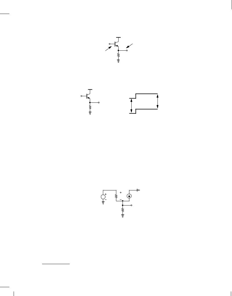
Another important circuit topology is the emitter follower (also called the “common-collector” stage). The reader is encouraged to review Examples 5.2 - 5.3, rules illustrated in Fig. 5.7, and the possible topologies in Fig. 5.28 before proceeding further. For the sake of brevity, we may also use the term “follower” to refer to emitter followers in this chapter.
Shown in Fig. 5.83, the emitter follower senses the input at the base of the transistor and produces the output at the emitter. The collector is tied to VCC and hence ac ground. We first study the core and subsequently add the biasing elements.
Emitter Follower Core How does the follower in Fig. 5.84(a) respond to a change in Vin? If Vin rises by a small amount Vin, the base-emitter voltage of Q1 tends to increase, raising the collector and emitter currents. The higher emitter current translates to a greater drop across RE and hence a higher Vout. From another perspective, if we assume, for example, Vout is constant, then VBE must rise and so must IE, requiring that Vout go up. Since Vout changes in the same
BR |
Wiley/Razavi/Fundamentals of Microelectronics [Razavi.cls v. 2006] |
June 30, 2007 at 13:42 |
245 (1) |
|
|
|
|
Sec. 5.3 |
Bipolar Amplifier Topologies |
|
245 |
|
|
VCC |
Output Sensed |
|
Vin |
Q 1 |
|
|
at Emitter |
||
|
Input Applied |
|
Vout |
|
to Base |
RE |
|
Figure 5.83 Emitter follower.
direction as Vin, we expect the voltage gain to be positive. Note that Vout is always lower than Vin by an amount equal to VBE, and the circuit is said to provide “level shift.”
|
VCC |
|
|
Vin1 + |
V in |
Vin |
Q 1 |
|
Vin1 |
|
VBE2 |
|
|
Vout |
|
||
|
|
VBE1 |
Vout1 + |
||
|
|
Vout |
|||
|
RE |
|
|||
|
|
Vout1 |
|
|
|
|
|
|
|
|
|
|
(a) |
|
|
(b) |
|
Figure 5.84 (a) Emitter follower sensing an input change, (b) response of the circuit.
Another interesting and important observation here is that the change in Vout cannot be larger than the change in Vin. Suppose Vin increases from Vin1 to Vin1 + Vin and Vout from Vout1 to Vout1 + Vout [Fig. 5.84(b)]. If the output changes by a greater amount than the input, Vout >Vin, then VBE2 must be less than VBE1. But this means the emitter current also decreases and so does IERE = Vout, contradicting the assumption that Vout has increased. Thus, Vout <Vin, implying that the follower exhibits a voltage gain less than unity.15
The reader may wonder if an amplifier with a subunity gain has any practical value. As explained later, the input and output impedances of the emitter follower make it a particularly useful circuit for some applications.
Let us now derive the small-signal properties of the follower, first assuming VA = 1. Shown in Fig. 5.85, the equivalent circuit yields
v in |
r π vπ |
gm vπ |
|
|
v out |
|
|
RE |
Figure 5.85 Small-signal model of emitter follower. |
|
|
v + g |
v |
= vout |
(5.317) |
||||
r |
|
|
m |
|
RE |
|
|
|
|
|
|
|
|
||
and hence |
|
|
|
|
|
|
|
v |
= |
|
r |
|
vout : |
(5.318) |
|
|
|
|
|||||
|
|
+ 1 |
|
RE |
|
||
15In an extreme case described in Example 5.43, the gain becomes equal to unity.

BR |
Wiley/Razavi/Fundamentals of Microelectronics [Razavi.cls v. 2006] |
June 30, 2007 at 13:42 |
246 (1) |
|
|
|
|
246 |
Chap. 5 |
Bipolar Amplifiers |
We also have
vin = v + vout:
Substituting for v from (5.318), we obtain
vout = |
|
1 |
|
|
|
|
|
|
r |
|
1 |
|
|||
vin |
1 + |
|
|||||
|
+ 1 |
RE |
|||||
|
RE |
: |
|
|
|||
|
1 |
|
|
|
|||
|
RE + |
|
|
|
|
|
|
|
gm |
|
|
|
|||
The voltage gain is therefore positive and less than unity.
(5.319)
(5.320)
(5.321)
Example 5.43
In integrated circuits, the follower is typically realized as shown in Fig. 5.86. Determine the voltage gain if the current source is ideal and VA = 1.
VCC
Vin

 Q 1
Q 1

 Vout
Vout
 I 1
I 1
Figure 5.86 Follower with current source.
Solution
Since the emitter resistor is replaced with an ideal current source, the value of RE in Eq. (5.321) must tend to infinity, yielding
Av = 1: |
(5.322) |
This result can also be derived intuitively. A constant current source flowing through Q1 requires that VBE = VT ln(IC=IS) remain constant. Writing Vout = Vin , VBE, we recognize that Vout exactly follows Vin if VBE is constant.
Exercise
Repeat the above example if a resistor of value R1 is placed in series with the collector.
Equation (5.321) suggests that the emitter follower acts as a voltage divider, a perspective that can be reinforced by an alternative analysis. Suppose, as shown in Fig. 5.87(a), we wish to model vin and Q1 by a Thevenin equivalent. The Thevenin voltage is given by the open-circuit output voltage produced by Q1 [Fig. 5.87(b)], as if Q1 operates with RE = 1 (Example 5.43). Thus, vT hev = vin. The Thevenin resistance is obtained by setting the input to zero [Fig. 5.87(c)] and is equal to 1=gm. The circuit of Fig. 5.87(a) therefore reduces to that shown in Fig. 5.87(d), confirming operation as a voltage divider.

BR |
Wiley/Razavi/Fundamentals of Microelectronics [Razavi.cls v. 2006] |
June 30, 2007 at 13:42 |
247 (1) |
|
|
|
|
Sec. 5.3 |
Bipolar Amplifier Topologies |
|
|
247 |
|
VCC |
|
|
VCC |
|
Q 1 |
|
Q 1 |
|
|
v in |
v out |
v in |
v out = v in |
|
|
RE |
|
|
|
(a) |
|
(b) |
|
|
VCC |
|
RThev = |
1 |
|
|
|
|
g m |
|
Q 1 |
|
|
v out |
|
|
|
v Thev = v in |
RE |
|
|
|
|
|
|
R Thev |
|
|
|
|
(c) |
|
(d) |
|
Figure 5.87 (a) Emitter follower stage, (b) Thevenin voltage , (c) Thevenin resistance, (d) simplified circuit.
Example 5.44
Determine the voltage gain of a follower driven by a finite source impedance of RS [Fig. 5.88(a)] |
|||||||||||||||||||||||||||||||||||||
if VA = 1. |
|
|
|
|
|
|
|
|
|
|
|
|
|
|
|
|
|
||||||||||||||||||||
|
|
|
|
|
|
RS |
|
|
|
|
|
VCC |
|
|
|
|
|
|
|
RS |
|
|
|
|
VCC |
||||||||||||
|
|
|
|
|
|
|
|
|
|
|
|
|
|
|
|||||||||||||||||||||||
v in |
|
|
|
|
|
|
Q 1 |
v out |
|
|
|
|
|
|
Q 1 |
||||||||||||||||||||||
|
|
||||||||||||||||||||||||||||||||||||
|
|
|
|
|
|
|
|
|
|
|
|
|
|
|
|
|
|||||||||||||||||||||
|
|
|
|
|
|
|
|
|
|
||||||||||||||||||||||||||||
|
|
|
|
|
|
|
|
|
|
|
|
|
|
|
|
|
|
|
|||||||||||||||||||
|
|
|
|
|
|
|
|
RE |
|
|
|
|
|
|
|
|
|||||||||||||||||||||
|
|
|
|
|
|
|
|
|
|
|
|
|
|
|
|
|
|
|
|
|
|
|
|
|
|
|
|
|
|
|
|
|
|
|
|||
|
|
|
|
|
|
|
|
|
|
|
|
|
|
|
|
|
|
|
|
|
|
|
|
|
|
|
|
|
|
|
|
|
|
|
|||
|
|
|
|
|
|
|
|
|
|
|
|
|
|
|
|
|
|
|
|
|
|
|
|
|
|
|
|
|
|
|
|
|
|
|
R Thev |
||
|
|
|
|
|
|
|
|
|
|
|
|
|
|
|
|
|
|
|
|
|
|
|
|||||||||||||||
|
|
|
|
|
|
|
|
|
|
|
|
|
|
|
|
|
|
|
|
|
|
|
|||||||||||||||
|
|
|
|
|
|
|
|
|
|
(a) |
|
|
|
|
|
|
|
|
|
|
|
|
(b) |
||||||||||||||
|
1 |
|
+ |
RS |
|
||||||||||||||||||||||||||||||||
|
|
|
|
|
|
|
|
|
|
|
|
|
|
|
|
|
|
|
|
|
|
β+ 1 |
|||||||||||||||
|
|
|
|
|
|
|
|
|
|
|
|
|
|
|
|
|
|
|
g m |
||||||||||||||||||

 v out v Thev = v in RE
(c)
Figure 5.88 (a) Follower with source impedance, (b) Thevenin resistance seen at emitter, (c) simplified circuit.
Solution
We model vin, RS, and Q1 by a Thevenin equivalent. The reader can show that the open-circuit voltage is equal to vin. Furthermore, the Thevenin resistance [Fig. 5.88(b)] is given by (5.291) as RS=( + 1) + 1=gm. Figure 5.88(c) depicts the equivalent circuit, revealing that
vout = |
|
RE |
|
|
|
: |
(5.323) |
|
|
RS |
|
|
1 |
|
|||
vin |
RE + |
|
|
|
||||
|
+ 1 |
+ |
gm |
|
|
|
||
This result can also be obtained by solving the small-signal equivalent circuit of the follower.

BR |
Wiley/Razavi/Fundamentals of Microelectronics [Razavi.cls v. 2006] |
June 30, 2007 at 13:42 |
248 (1) |
|
|
|
|
248 |
Chap. 5 |
Bipolar Amplifiers |
Exercise
What happens if RE = 1?
In order to appreciate the usefulness of emitter followers, let us compute their input and output impedances. In the equivalent circuit of Fig. 5.89(a), we have iX r = v . Also, the current iX and gmv flow through RE, producing a voltage drop equal to (iX + gmv )RE. Adding the voltages across r and RE and equating the result to vX , we have
|
i X |
|
VCC |
|
VCC |
|
|
RC |
0 |
|
|
|
|
|
|
||
v X |
r π vπ |
gm vπ |
Q 1 |
|
Q 1 |
|
|
|
|
||
|
RE |
R in |
RE |
R in |
RE |
|
(a) |
|
|
(b) |
|
Figure 5.89 (a) Input impedance of emitter follower, (b) equivalence of CE and follower stages.
vX = v + (iX + gmv )RE |
(5.324) |
|
= iX r + (iX + gmiXr )RE; |
(5.325) |
|
and hence |
|
|
vX = r |
+ (1 + )R : |
(5.326) |
|
E |
|
iX |
|
|
This expression is identical to that in Eq. (5.162) derived for a degenerated CE stage. This is, of course, no coincidence. Since the input impedance of the CE topology is independent of the collector resistor (for VA = 1), its value remains unchanged if RC = 0, which is the case for an emitter follower [Fig. 5.89(b)].
The key observation here is that the follower “transforms” the load resistor, RE, to a much larger value, thereby serving as an efficient “buffer.” This concept can be illustrated by an example.
Example 5.45
A CE stage exhibits a voltage gain of 20 and an output resistance of 1 k . Determine the voltage gain of the CE amplifier if
(a)The stage drives an 8- speaker directly.
(b)An emitter follower biased at a current of 5 mA is interposed between the CE stage and the speaker. Assume = 100, VA = 1, and the follower is biased with an ideal current source.
Solution
(a) As depicted in Fig. 5.90(a), the equivalent resistance seen at the collector is now given by the parallel combination of RC and the speaker impedance, Rsp, reducing the gain from 20 to 20 (RCjj8 )=RC = 0:159. The voltage gain therefore degrades drastically.

BR |
Wiley/Razavi/Fundamentals of Microelectronics [Razavi.cls v. 2006] |
June 30, 2007 at 13:42 |
249 (1) |
|
|
|
|
Sec. 5.3 Bipolar Amplifier Topologies |
|
|
249 |
|
VCC |
|
VCC |
||
1 kΩ RC |
|
1 kΩ RC |
|
|
Rsp |
|
Q 2 |
|
|
Q 1 C1 |
|
|
||
|
Q 1 |
Rsp |
||
v in |
v in |
R in1 |
C1 |
|
I |
||||
|
|
1 |
||
(a) |
|
(b) |
|
|
Figure 5.90 (a) CE stage and (b) two-stage circuit driving a speaker.
(b) From the arrangement in Fig. 5.90(b), we note that |
|
Rin1 = r 2 + ( + 1)Rsp |
(5.327) |
= 1058 : |
(5.328) |
Thus, the voltage gain of the CE stage drops from 20 to 20 (RCjjRin1)=RC |
= 10:28, a |
substantial improvement over case (a). |
|
Exercise
Repeat the above example if the emitter follower is biased at a current of 10 mA.
We now calculate the output impedance of the follower, assuming the circuit is driven by a source impedance RS [Fig. 5.91(a)]. Interestingly, we need not resort to a small-signal model here as Rout can be obtained by inspection. As illustrated in Fig. 5.91(b), the output resistance can be viewed as the parallel combination of two components: one seen looking “up” into the emitter and another looking “down” into RE. From Fig. 5.88, the former is equal to RS=( + 1) + 1=gm, and hence
VCC |
VCC |
|
|
|
RS |
RS |
|
|
|
Q 1 |
Q 1 |
|
|
|
|
1 |
+ |
RS |
|
R E |
g m |
β+ 1 |
||
|
||||
R out |
R E |
|
|
|
|
R E |
|
|
|
(a) |
(b) |
|
|
Figure 5.91 (a) Output impedance of a follower, (b) components of output resistance.
R |
out |
= |
RS |
|
+ |
1 |
jjR : |
(5.329) |
|
|
|||||||
|
|
|
+ 1 |
|
gm |
|
||
This result can also be derived from the Thevenin equivalent shown in Fig. 5.88(c) by setting vin to zero.

BR |
Wiley/Razavi/Fundamentals of Microelectronics [Razavi.cls v. 2006] |
June 30, 2007 at 13:42 |
250 (1) |
|
|
|
|
250 |
Chap. 5 |
Bipolar Amplifiers |
Equation (5.329) reveals another important attribute of the follower: the circuit transforms the source impedance, RS, to a much lower value, thereby providing higher “driving” capability. We say the follower operates as a good “voltage buffer” because it displays a high input impedance (like a voltmeter) and a low output impedance (like a voltage source).
Effect of Transistor Output Resistance Our analysis of the follower has thus far neglected the Early effect. Fortunately, the results obtained above can be readily modified to reflect this nonideality. Figure 5.92 illustrates a key point that facilitates the analysis: in small-signal operation, rO appears in parallel with RE. We can therefore rewrite Eqs. (5.323), (5.326) and (5.329) as
VCC
RS


 r O v in Q 1

R E
Figure 5.92 Follower including transistor output resistance.
RS |
|
Q 1 |
|
v in |
|
R E |
r O |
Av = |
|
|
|
REjjrO |
|
|
|
|
(5.330) |
|||
|
|
|
|
|
|
RS |
1 |
|
|
|||
|
REjjrO + |
|
|
|
+ |
|
|
|
||||
|
+ 1 |
gm |
|
|||||||||
Rin = r + ( + 1)(REjjrO) |
(5.331) |
|||||||||||
R = |
RS |
|
+ |
1 |
jjR |
jjr : |
(5.332) |
|||||
|
|
|||||||||||
out |
|
+ 1 |
|
|
gm |
E |
|
O |
|
|||
|
|
|
|
|
|
|
|
|
||||
Example 5.46
Determine the small-signal properties of an emitter follower using an ideal current source (as in Example 5.43) but with a finite source impedance RS.
Solution
Since RE = 1, we have
Av
Rin
Rout
Also, gmrO 1, and hence
= |
|
|
|
|
|
rO |
|
|
|
|
|
|
|
|
|
rO + |
|
RS |
|
+ |
1 |
|
|
||||||||
|
|
|
|
|
|||||||||||
|
+ 1 |
gm |
|||||||||||||
|
|
|
|
|
|
||||||||||
= r + ( + 1)rO ) |
|||||||||||||||
= |
RS |
|
+ |
|
1 |
jjr : |
|||||||||
|
|
|
|
|
|||||||||||
|
|
+ 1 |
|
gm |
|
|
|
|
O |
||||||
|
|
|
|
|
|
|
|
||||||||
Av |
|
|
|
rO |
|
|
|
|
|
|
|
||||
rO + |
|
RS |
|
|
|
|
|
||||||||
|
|
|
|
|
|
|
|
|
|||||||
|
|
|
+ 1 |
||||||||||||
|
|
|
|
|
|
|
|||||||||
Rin ( + 1)rO:
(5.333)
(5.334)
(5.335)
(5.336)
(5.337)