

Fundamentals of Microelectronics
.pdfBR |
Wiley/Razavi/Fundamentals of Microelectronics [Razavi.cls v. 2006] |
June 30, 2007 at 13:42 |
121 (1) |
|
|
|
|
Sec. 3.6 |
Chapter Summary |
121 |
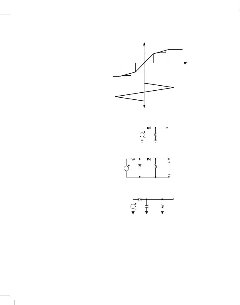
45.In the limiting circuit of Fig. 3.51, plot the currents flowing through D1 and D2 as a function of time if the input is given by V0 cos !t and V0 > VD;on + VB1 and ,V0 > ,VD;on , VB2.
46.Design the limiting circuit of Fig. 3.51 for a negative threshold of ,1:9 V and a positive threshold of +2:2 V. Assume the input peak voltage is equal to 5 V, the maximum allowable current through each diode is 2 mA, and VD;on 800 mV.
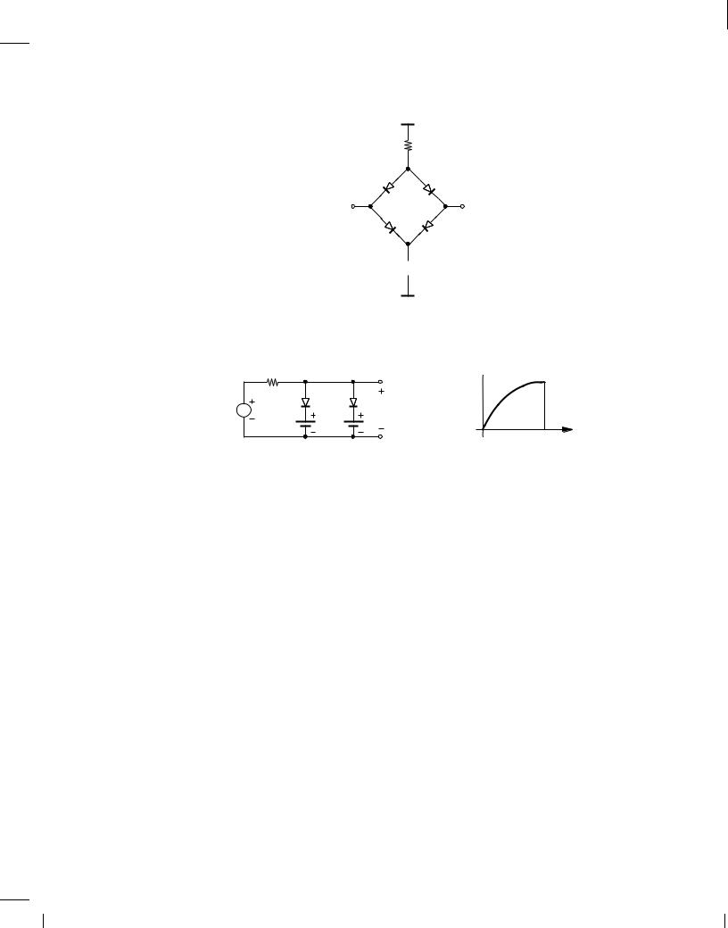
47.We wish to design a circuit that exhibits the input/output characteristic shown in Fig. 3.83. Using 1-k resistors, ideal diodes, and other components, construct the circuit.
Vout |
|
|
+ 2 V |
|
0.5 |
|
|
|
− 2 V |
|
|
|
+ 2 V |
Vin |
|
|
|
|
− 2 V |
|
0.5
Figure 3.83
48.“Wave-shaping” applications require the input/output characteristic illustrated in Fig. 3.84. Using ideal diodes and other components, construct a circuit that provides such a character-
|
Vout |
|
|
|
+ 2 V |
0.5 |
|
|
|
|
|
−4 V |
− 2 V |
|
|
|
+ 2 V |
+ 4 V |
Vin |
|
|
|
|
|
− 2 V |
|
|
0.5
Figure 3.84
istic. (The value of resistors is not unique.)
49.Suppose a triangular waveform is applied to the characteristic of Fig. 3.84 as shown in Fig. 3.85. Plot the output waveform and note that it is a rough approximation of a sinusoid. How should the input-output characteristic be modified so that the output becomes a better approximation of a sinusoid?
SPICE Problems
In the following problems, assume IS = 5 10,16 A.
50.The half-wave rectifier of Fig. 3.86 must deliver a current of 5 mA to R1 for a peak input level of 2 V.
(a) Using hand calculations, determine the required value of R1.
(b) Verify the result by SPICE.
51.In the circuit of Fig. 3.87, R1 = 500 and R2 = 1 k . Use SPICE to construct the input/output characteristic for ,2 V < Vin < +2 V. Also, plot the current flowing through R1 as a function of Vin.
52.The rectifier shown in Fig. 3.88 is driven by a 60-Hz sinusoid input with a peak amplitude of 5 V. Using the transient analysis in SPICE,
BR |
Wiley/Razavi/Fundamentals of Microelectronics [Razavi.cls v. 2006] |
June 30, 2007 at 13:42 |
122 (1) |
|
|
|
|
122 |
|
|
Chap. 3 |
Diode Models and Circuits |
||
|
|
Vout |
|
|
|
|
|
|
+ 2 V |
0.5 |
|
|
|
|
|
|
|
|
||
|
−4 V |
− 2 V |
|
|
|
|
|
|
|
+ 2 V |
+ 4 V |
Vin |
|
|
|
|
|
|
||
|
|
|
− 2 V |
|
|
|
|
|
0.5 |
|
Vin |
|
|
|
|
|
|
|
|
|
t |
|
|
|
Figure 3.85 |
|
|
|
|
D1 |
|
|
|
|
|
Vout |
Vin |
|
R1 |
|
Figure 3.86 |
|
|
|
R1 |
D1 |
|
|
D2 |
|
R2 |
Vout |
in |
|
|
|
Figure 3.87 |
|
|
|
D1 |
|
|
|
|
|
|
Vout |
Vin |
1 µF |
|
100Ω |
Figure 3.88
(a)Determine the peak-to-peak ripple at the output.
(b)Determine the peak current flowing through D1.
(c)Compute the heaviest load (smallest RL) that the circuit can drive while maintaining a ripple less than 200 mVpp.
53.The circuit of Fig. 3.89 is used in some analog circuits. Plot the input/output characteristic for
,2 V < Vin < +2 V and determine the maximum input range across which jVin,Voutj < 5 mV.
54.The circuit shown in Fig. 3.90 can provide an approximation of a sinusoid at the output in response to a triangular input waveform. Using the dc analysis in SPICE to plot the input/output characteristic for 0 < Vin < 4 V, determine the values of VB1 and VB2 such that
BR |
Wiley/Razavi/Fundamentals of Microelectronics [Razavi.cls v. 2006] |
June 30, 2007 at 13:42 |
123 (1) |
|
|
|
|
Sec. 3.6 |
Chapter Summary |
123 |
|
|
VCC = +2.5 V |
|
|
1 kΩ |
|
D 2 |
D 3 |
|
Vin |
Vout |
D 4
Figure 3.89
the characteristic closely resembles a sinusoid.
Ω |
|
|
|
2 k |
|
|
|
D1 |
D |
2 |
Vout |
Vin |
VB2 |
|
|
VB1 |
|
|
(a)
Figure 3.90
D 1
 1 kΩ
1 kΩ
VEE = −2.5 V
Vout 
4 V Vin
(b)
BR |
Wiley/Razavi/Fundamentals of Microelectronics [Razavi.cls v. 2006] |
June 30, 2007 at 13:42 |
124 (1) |
|
|
|
|
Physics of Bipolar Transistors
The bipolar transistor was invented in 1945 by Shockley, Brattain, and Bardeen at Bell Laboratories, subsequently replacing vacuum tubes in electronic systems and paving the way for integrated circuits.
In this chapter, we analyze the structure and operation of bipolar transistors, preparing ourselves for the study of circuits employing such devices. Following the same thought process as in Chapter 2 for pn junctions, we aim to understand the physics of the transistor, derive equations that represent its I/V characteristics, and develop an equivalent model that can be used in circuit analysis and design. Figure 4 illustrates the sequence of concepts introduced in this chapter.
|
|
|
|
|
|
|
|
|
|
|
|
|
|
|
Voltage−Controlled |
|
|
Structure of |
|
|
Operation of |
|
|
Large−Signal |
|
|
Small−Signal |
|
Device as Amplifying |
|
|
|
|
|
|
|
|
||||
|
|
|
Bipolar Transistor |
|
|
Bipolar Transistor |
|
|
Model |
|
|
Model |
|
|
Element |
|
|
|
|
|
|
|
|
||||
|
|
|
|
|
|
|
|
|
|
|
|
|
|
|
|
|
|
|
|
|
|
|
|
|
|
|
|
4.1 General Considerations
In its simplest form, the bipolar transistor can be viewed as a voltage-dependent current source. We first show how such a current source can form an amplifier and hence why bipolar devices are useful and interesting.
Consider the voltage-dependent current source depicted in Fig. 4.1(a), where I1 is proportional to V1: I1 = KV1. Note that K has a dimension of resistance,1. For example, with K = 0:001 ,1, an input voltage of 1 V yields an output current of 1 mA. Let us now construct the circuit shown in Fig. 4.1(b), where a voltage source Vin controls I1 and the output current flows through a load resistor RL, producing Vout. Our objective is to demonstrate that this circuit can operate as an amplifier, i.e., Vout is an amplified replica of Vin. Since V1 = Vin and Vout = ,RLI1, we have
Vout = ,KRLVin: |
(4.1) |
Interestingly, if KRL > 1, then the circuit amplifies the input. The negative sign indicates that the output is an “inverted” replica of the input circuit [Fig. 4.1(b)]. The amplification factor or “voltage gain” of the circuit, AV , is defined as
AV = |
Vout |
(4.2) |
|
Vin |
|
= ,KRL; |
(4.3) |
|
124
BR |
Wiley/Razavi/Fundamentals of Microelectronics [Razavi.cls v. 2006] |
June 30, 2007 at 13:42 |
125 (1) |
|
|
|
|
Sec. 4.1 |
General Considerations |
|
|
|
|
|
|
|
|
125 |
||
|
|
|
|
|
|
|
|
|
|
|
|
Vp |
|
|
|
|
|
|
|
|
|
|
|
|
Vin |
|
|
|
|
|
|
|
|
|
|
|
|
t |
V |
I |
|
KV |
V |
|
V |
I |
|
KV |
V |
|
K RLVp |
1 |
|
1 |
1 |
|
in |
1 |
|
1 |
1 |
RL |
out |
Vout |
|
|
|
|
|
|
|
|
|
|
|
|
t |
|
(a) |
|
|
|
|
|
|
|
(b) |
|
|
|
Figure 4.1 (a) Voltage-dependent current source, (b) simple amplifier.
and depends on both the characteristics of the controlled current source and the load resistor. Note that K signifies how strongly V1 controls I1, thus directly affecting the gain.
Example 4.1
Consider the circuit shown in Fig. 4.2, where the voltage-controlled current source exhibits an “internal” resistance of rin. Determine the voltage gain of the circuit.
Vin |
r in V1 I 1 KV1 RL Vout |
Figure 4.2 Voltage-dependent current source with an internal resistance rin.
Solution
Since V1 is equal to Vin regardless of the value of rin, the voltage gain remains unchanged. This point proves useful in our analyses later.
Exercise
Repeat the above example if rin = 1.
The foregoing study reveals that a voltage-controlled current source can indeed provide signal amplification. Bipolar transistors are an example of such current sources and can ideally be modeled as shown in Fig. 4.3. Note that the device contains three terminals and its output current is an exponential function of V1. We will see in Section 4.4.4 that under certain conditions, this model can be approximated by that in Fig. 4.1(a).
As three-terminal devices, bipolar transistors make the analysis of circuits more difficult. Having dealt with two-terminal components such as resistors, capacitors, inductors, and diodes in elementary circuit analysis and the previous chapters of this book, we are accustomed to a one- to-one correspondence between the current through and the voltage across each device. With three-terminal elements, on the other hand, one may consider the current and voltage between every two terminals, arriving at a complex set of equations. Fortunately, as we develop our understanding of the transistor's operation, we discard some of these current and voltage combinations as irrelevant, thus obtaining a relatively simple model.
BR |
Wiley/Razavi/Fundamentals of Microelectronics [Razavi.cls v. 2006] |
June 30, 2007 at 13:42 |
126 (1) |
|
|
|
|
126 |
|
Chap. 4 |
Physics of Bipolar Transistors |
1 |
|
V1 |
3 |
V |
|
|
|
1 |
I S exp |
|
|
|
VT |
|
|
|
|
|
2
Figure 4.3 Exponential voltage-dependent current source.
4.2 Structure of Bipolar Transistor
The bipolar transistor consists of three doped regions forming a sandwich. Shown in Fig. 4.4(a) is an example comprising of a p layer sandwiched between two n regions and called an “ npn” transistor. The three terminals are called the “base,” the “emitter,” and the “collector.” As explained later, the emitter “emits” charge carriers and the collector “collects” them while the base controls the number of carriers that make this journey. The circuit symbol for the npn transistor is shown in Fig. 4.4(b). We denote the terminal voltages by VE, VB, and VC , and the voltage differences by VBE, VCB, and VCE. The transistor is labeled Q1 here.
|
Collector |
|
Collector |
|
|
(C) |
|
|
|
|
|
|
n |
|
VCB |
|
|
Base |
|
Base |
p |
Q 1 VCE |
|
|
|
(B) |
|
|
n |
|
VBE |
|
Emitter |
|
Emitter |
|
|
(E) |
|
|
|
|
|
|
(a) |
|
(b) |
Figure 4.4 (a) Structure and (b) circuit symbol of bipolar transistor.
We readily note from Fig. 4.4(a) that the device contains two pn junction diodes: one between the base and the emitter and another between the base and the collector. For example, if the base is more positive than the emitter, VBE > 0, then this junction is forward-biased. While this simple diagram may suggest that the device is symmetric with respect to the emitter and the collector, in reality, the dimensions and doping levels of these two regions are quite different. In
other words, E and C cannot be interchanged. We will also see that proper operation requires a
thin base region, e.g., about 100 A in modern integrated bipolar transistors.
As mentioned in the previous section, the possible combinations of voltages and currents for a three-terminal device can prove overwhelming. For the device in Fig. 4.4(a), VBE, VBC, and VCE can assume positive or negative values, leading to 23 possibilities for the terminal voltages of the transistor. Fortunately, only one of these eight combinations finds practical value and comes into our focus here.
Before continuing with the bipolar transistor, it is instructive to study an interesting effect in pn junctions. Consider the reverse-biased junction depicted in Fig. 4.5(a) and recall from Chapter 2 that the depletion region sustains a strong electric field. Now suppose an electron is somehow “injected” from outside into the right side of the depletion region. What happens to this electron? Serving as a minority carrier on the p side, the electron experiences the electric field and is rapidly
BR |
Wiley/Razavi/Fundamentals of Microelectronics [Razavi.cls v. 2006] |
June 30, 2007 at 13:42 |
127 (1) |
|
|
|
|
Sec. 4.3 Operation of Bipolar Transistor in Active Mode 127
swept away into the n side. The ability of a reverse-biased pn junction to efficiently “collect” externally-injected electrons proves essential to the operation of the bipolar transistor.
|
|
|
|
|
|
Electron injected |
|
|
|
|||||||||||
|
|
|
|
|
|
|
|
|
|
|
|
|
|
|
|
|
|
|
|
|
|
|
|
|
|
|
|
|
|
|
e |
|
|
|
|
|
|
|
|
||
|
|
|
|
|
n |
|
|
|
|
|
|
|
|
p |
|
|
|
|
|
|
|
|
|
|
|
|
|
|
|
|
|
|
|
|
|
|
|
|
|
|
|
|
|
− |
|
− |
|
− |
|
+ |
− |
+ |
|
+ |
|
+ |
|
|
|
|||
|
− |
− |
− |
− |
− |
− |
− |
+ |
− |
+ |
+ |
+ |
+ |
+ |
+ |
+ |
|
|||
|
− |
− |
− |
− |
− |
− |
− |
+ |
− |
+ |
+ |
+ |
+ |
+ |
+ |
+ |
|
|||
|
|
|||||||||||||||||||
|
− |
− |
− |
− |
+ − |
+ |
+ |
+ |
+ |
|
||||||||||
|
− |
− |
− |
+ |
+ |
+ |
|
|||||||||||||
|
− |
− |
− |
− + − + |
+ |
+ |
+ |
|
||||||||||||
|
|
|
|
|
|
|
|
|
|
|
|
|
|
|
|
|
|
|
|
|
|
|
|
|
|
|
|
|
|
|
|
|
|
|
|
|
|
|
|
|
|
E
VR
Figure 4.5 Injection of electrons into depletion region.
4.3 Operation of Bipolar Transistor in Active Mode
In this section, we analyze the operation of the transistor, aiming to prove that, under certain conditions, it indeed acts as a voltage-controlled current source. More specifically, we intend to show that (a) the current flow from the emitter to the collector can be viewed as a current source tied between these two terminals, and (b) this current is controlled by the voltage difference between the base and the emitter, VBE.
We begin our study with the assumption that the base-emitter junction is forward-biased (VBE > 0) and the base-collector junction is reverse-biased (VBC < 0). Under these conditions, we say the device is biased in the “forward active region” or simply in the “active mode.” For example, with the emitter connected to ground, the base voltage is set to about 0.8 V and the collector voltage to a higher value, e.g., 1 V [Fig. 4.6(a)]. The base-collector junction therefore
experiences a reverse bias of 0.2 V.
I 2
|
VCE = +1 V |
|
|
D2 |
|
VBE |
|
|
VCE = +1 V |
||
= +0.8 V |
= +0.8 V |
|
|||
I 1 |
D1 |
||||
|
VBE |
||||
|
(a) |
|
|
(b) |
Figure 4.6 (a) Bipolar transistor with base and collector bias voltages, (b) simplistic view of bipolar transistor.
Let us now consider the operation of the transistor in the active mode. We may be tempted to simplify the example of Fig. 4.6(a) to the equivalent circuit shown in Fig. 4.6(b). After all, it appears that the bipolar transistor simply consists of two diodes sharing their anodes at the base terminal. This view implies that D1 carries a current and D2 does not; i.e., we should anticipate current flow from the base to the emitter but no current through the collector terminal. Were this true, the transistor would not operate as a voltage-controlled current source and would prove of little value.
To understand why the transistor cannot be modeled as merely two back-to-back diodes, we must examine the flow of charge inside the device, bearing in mind that the base region is very
BR |
Wiley/Razavi/Fundamentals of Microelectronics [Razavi.cls v. 2006] |
June 30, 2007 at 13:42 |
128 (1) |
|
|
|
|
128 |
Chap. 4 |
Physics of Bipolar Transistors |
thin. Since the base-emitter junction is forward-biased, electrons flow from the emitter to the base and holes from the base to the emitter. For proper transistor operation, the former current component must be much greater than the latter, requiring that the emitter doping level be much greater than that of the base (Chapter 2). Thus, we denote the emitter region with n+, where the superscript emphasizes the high doping level. Figure 4.7(a) summarizes our observations thus far, indicating that the emitter injects a large number of electrons into the base while receiving a small number of holes from it.
|
n |
Depletion |
|
n |
|
VCE = +1 V |
Region |
|
VCE = +1 V |
|
p |
|
|
p |
VBE = +0.8 V |
− |
VBE = +0.8 V |
h+ |
e− |
h+ |
e |
|
n + |
|
|
n + |
|
|
(a) |
(b) |
Depletion |
n |
Region |
VCE = +1 V |
e− |
p |
VBE = +0.8 V |
|
h+ |
n + |
|
(c)
Figure 4.7 (a) Flow of electrons and holes through base-emitter junction, (b) electrons approaching collector junction, (c) electrons passing through collector junction.
What happens to electrons as they enter the base? Since the base region is thin, most of the electrons reach the edge of the collector-base depletion region, beginning to experience the built-in electric field. Consequently, as illustrated in Fig. 4.5, the electrons are swept into the collector region (as in Fig. 4.5) and absorbed by the positive battery terminal. Figures 4.7(b) and
(c) illustrate this effect in “slow motion.” We therefore observe that the reverse-biased collectorbase junction carries a current because minority carriers are “injected” into its depletion region.
Let us summarize our thoughts. In the active mode, an npn bipolar transistor carries a large number of electrons from the emitter, through the base, to the collector while drawing a small current of holes through the base terminal. We must now answer several questions. First, how do electrons travel through the base: by drift or diffusion? Second, how does the resulting current depend on the terminal voltages? Third, how large is the base current?
Operating as a moderate conductor, the base region sustains but a small electric field, i.e., it allows most of the field to drop across the base-emitter depletion layer. Thus, as explained for pn junctions in Chapter 2, the drift current in the base is negligible,1 leaving diffusion as the principal mechanism for the flow of electrons injected by the emitter. In fact, two observations directly lead to the necessity of diffusion: (1) redrawing the diagram of Fig. 2.29 for the emitterbase junction [Fig. 4.8(a)], we recognize that the density of electrons at x = x1 is very high; (2)
1This assumption simplifies the analysis here but may not hold in the general case.
BR |
Wiley/Razavi/Fundamentals of Microelectronics [Razavi.cls v. 2006] |
June 30, 2007 at 13:42 |
129 (1) |
|
|
|
|
Sec. 4.3 |
Operation of Bipolar Transistor in Active Mode |
129 |
since any electron arriving at x = x2 in Fig. 4.8(b) is swept away, the density of electrons falls to zero at this point. As a result, the electron density in the base assumes the profile depicted in Fig. 4.8(c), providing a gradient for the diffusion of electrons.
VBE
e
h
Forward
Biased
(a)
x |
|
|
|
Reverse |
|
|
|
|
|
|
|
|
x |
|||||||||||||||||||||||||||||
n |
|
|
|
|
VCE |
|
|
|
|
Biased |
|
|
|
|
|
|
|
|
n |
|
|
|
|
|
VCE |
|||||||||||||||||
|
|
|
|
|
|
|
|
|
|
|
|
|
|
|
|
|
|
|
|
|
|
|
|
|
|
|
|
|
|
|
|
|
|
|
|
|
|
|
|
|
||
p |
|
|
|
|
|
|
|
|
|
|
|
|
|
|
|
|
|
|
|
|
|
|
|
|
|
|
e |
p x2 |
|
|
|
|
|
|
|
|
||||||
|
|
|
|
|
|
|
|
|
|
|
|
|
|
|
|
|
|
|
|
|
|
|
||||||||||||||||||||
x1 |
VBE |
|
|
|
|
|
|
|
|
|
|
|
|
|
|
|
|
|
|
|
|
|
|
|
|
|
|
|
|
|
|
|||||||||||
|
|
|
|
|
|
|
|
|
|
|
|
|
|
|
|
|
|
|
|
|
|
|
|
|
|
|
|
|
|
|||||||||||||
|
|
|
|
|
|
|
|
|
|
|
|
|
|
|
|
|
|
|
|
|
|
|
|
|
|
|||||||||||||||||
n + |
|
|
|
|
|
|
|
|
|
|
|
|
|
|
|
|
|
|
n + |
|||||||||||||||||||||||
|
|
|
|
|
|
|
|
|
|
|
|
|
|
|
|
|
|
|||||||||||||||||||||||||
|
|
|
|
|
|
|
|
|
|
|
|
|
|
|
|
|
|
|||||||||||||||||||||||||
|
|
|
|
|
|
|
|
|
|
|
|
|
|
|
|
|
|
|
|
|
|
|
|
|
|
|
|
|
|
|
|
|
|
|
|
|
|
|
|
|
|
|
|
|
|
|
|
|
|
|
|
|
|
|
|
|
|
|
|
|
|
|
|
|
|
|
|
|
|
|
|
|
|
|
|
|
|
|
|
|
|
|
|
|
|
|
|
|
|
|
|
|
|
|
|
|
|
|
|
|
|
|
|
|
|
|
|
|
|
|
|
|
|
|
|
|
|
|
|
|
|
|
|
|
|
|
|
|
(b)
|
n |
x |
|
VCE |
|
|
|
|
e |
p |
x2 |
|
|
|
VBE |
n + |
x1 |
|
|
|
Electron |
|
|
Density |
|
|
(c)
Figure 4.8 (a) Hole and electron profiles at base-emitter junction, (b) zero electron density near collector,
(c) electron profile in base.
4.3.1 Collector Current
We now address the second question raised above and compute the current flowing from the collector to the emitter.2 As a forward-biased diode, the base-emitter junction exhibits a high concentration of electrons at x = x1 in Fig. 4.8(c) given by Eq. (2.96):
n(x1) = |
NE |
exp VBE , 1 |
(4.4) |
||
|
V0 |
||||
|
exp |
|
VT |
|
|
|
VT |
|
|
|
|
= |
NB |
exp |
VBE , 1 : |
(4.5) |
|
|
ni2 |
|
|
VT |
|
Here, NE and NB denote the doping levels in the emitter and the base, respectively, and we have
utilized the relationship exp(V0=VT ) = NENB=n2. In this chapter, we assume VT = 26 mV.
i
Applying the law of diffusion [Eq. (2.42)], we determine the flow of electrons into the collector as
J |
|
= qD |
|
dn |
|
(4.6) |
|
n |
|
n dx |
|
|
|
|
|
= qD |
n |
0 |
, n(x1); |
(4.7) |
|
|
|
|
WB |
|
|
|
|
|
|
|
|
|
2In an npn transistor, electrons go from the emitter to the collector. Thus, the conventional direction of the current is from the collector to the emitter.
BR |
Wiley/Razavi/Fundamentals of Microelectronics [Razavi.cls v. 2006] |
June 30, 2007 at 13:42 |
130 (1) |
|
|
|
|
130 |
Chap. 4 |
Physics of Bipolar Transistors |
where WB is the width of the base region. Multipling this quantity by the emitter cross section area, AE, substituting for n(x1) from (4.5), and changing the sign to obtain the conventional current, we obtain
I = |
AE qDnn2 |
VBE |
, 1 : |
i exp |
|
||
C |
NBWB |
VT |
|
|
|
In analogy with the diode current equation and assuming exp(VBE=VT ) 1, we write
IC = IS exp VBE ;
VT
where
IS = |
AEqDnn2 |
i : |
|
|
NBWB |
(4.8)
(4.9)
(4.10)
Equation (4.9) implies that the bipolar transistor indeed operates as a voltage-controlled current source, proving a good candidate for amplification. We may alternatively say the transistor performs “voltage-to-current conversion.”
Example 4.2
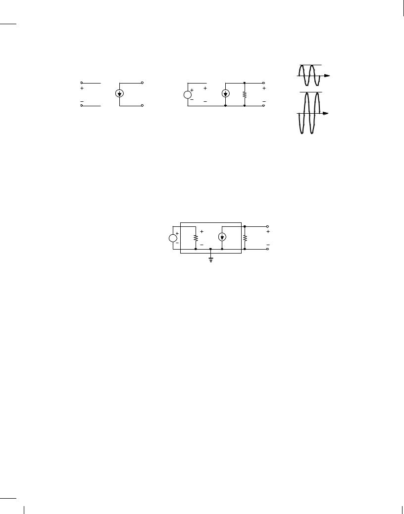
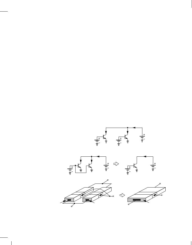
Determine the current IX in Fig. 4.9(a) if Q1 and Q2 are identical and operate in the active mode and V1 = V2.
|
|
I X |
|
I C1 |
I C2 |
|
Q1 |
Q 2 V3 |
|
V1 |
V2 |
|
|
(a) |
|
I X |
I X |
I C1 |
I C2 |
|
Q1 |
Q 2 V3 |
2A E V3 |
V1 |
|
V1 |
|
|
Qeq |
C
C
|
|
B |
B |
|
|
|
|
A E |
A E |
|
2A E |
|
E |
|
E |
|
|
|
(b)
Figure 4.9 (a) Two identical transistors drawing current from VC, (b) equivalence to a single transistor having twice the area.