

Fundamentals of Microelectronics
.pdfBR |
Wiley/Razavi/Fundamentals of Microelectronics [Razavi.cls v. 2006] |
June 30, 2007 at 13:42 |
61 (1) |
|
|
|
|
Diode Models and Circuits
Having studied the physics of diodes in Chapter 2, we now rise to the next level of abstraction and deal with diodes as circuit elements, ultimately arriving at interesting and real-life applications. This chapter also prepares us for understanding transistors as circuit elements in subsequent chapters. We proceed as follows:
Diodes as
Circuit Elements
 Ideal Diode
 Circuit Characteristics
 Actual Diode
Applications
 Regulators
 Rectifiers
 Limiting and Clamping Circuits
3.1 Ideal Diode
3.1.1 Initial Thoughts
In order to appreciate the need for diodes, let us briefly study the design of a cellphone charger. The charger converts the line ac voltage at 110 V1 and 60 Hz2 to a dc voltage of 3.5 V. As shown in Fig. 3.1(a), this is accomplished by first stepping down the ac voltage by means of a transformer to about 4 V and subsequently converting the ac voltage to a dc quantity.3 The same principle applies to adaptors that power other electronic devices.
How does the black box in Fig. 3.1(a) perform this conversion? As depicted in Fig. 3.1(b), the output of the transformer exhibits a zero dc content because the negative and positive half cycles enclose equal areas, leading to a zero average. Now suppose this waveform is applied to a mysterious device that passes the positive half cycles but blocks the negative ones. The result displays a positive average and some ac components, which can be removed by a low-pass filter (Section 3.5.1).
The waveform conversion in Fig. 3.1(b) points to the need for a device that discriminates between positive and negative voltages, passing only one and blocking the other. A simple resistor cannot serve in this role because it is linear. That is, Ohm's law, V = IR, implies that if the voltage across a resistor goes from positive to negative, so does the current through it. We must
1This value refers to the root-mean-square (rms) voltage. The peak value is therefore equal to 110p2.
2The line ac voltage in most countries is at 220 V and 50 Hz.
3The actual operation of adaptors is somewhat different.
61

BR |
Wiley/Razavi/Fundamentals of Microelectronics [Razavi.cls v. 2006] |
June 30, 2007 at 13:42 |
62 (1) |
|
|
|
|
62 |
|
|
Chap. 3 |
Diode Models and Circuits |
|
|
V1 |
|
60 Hz |
|
|
|
4 |
2 |
|
|
|
|
|
|
t |
|
|
Vline |
60 Hz |
|
|
|
|
110 |
2 |
|
Block |
3.5 V |
|
V1 |
Vout |
||||
|
t |
Box |
|||
|
|
t |
|||
|
|
|
|||
|
|
|
|
(a)
V1
4 2 |
? |
t |
t |
Positive Areas
Equal
Positive and Negative
Areas
(b)
Figure 3.1 (a) Charger circuit, (b) elimination of negative half cycles.
therefore seek a device that behaves as a short for positive voltages and as an open for negative voltages.
Figure 3.2 summarizes the result of our thought process thus far. The mysterious device generates an output equal to the input for positive half cycles and equal to zero for negative half cycles. Note that the device is nonlinear because it does not satisfy y = x; if x ! ,x, y 6! ,y.
y (t )
t
x (t )
t
Figure 3.2 Conceptual operation of a diode.
3.1.2 Ideal Diode
The mysterious device mentioned above is called an “ideal diode.” Shown in Fig. 3.3(a), the diode is a two-terminal device, with the triangular head denoting the allowable direction of current flow and the vertical bar representing the blocking behavior for currents in the opposite direction. The corresponding terminals are called the “anode” and the “cathode,” respectively.
Forward and Reverse Bias To serve as the mysterious device in the charger example of Fig. 3.3(a), the diode must turn “on” if Vanode > Vcathode and “off” if Vanode < Vcathode [Fig.

BR |
Wiley/Razavi/Fundamentals of Microelectronics [Razavi.cls v. 2006] |
June 30, 2007 at 13:42 |
63 (1) |
|
|
|
|
Sec. 3.1 |
Ideal Diode |
|
63 |
|
D 1 |
Forward Bias |
Reverse Bias |
Anode |
Cathode |
I X |
|
|
|
||
|
(a) |
|
(b) |
|
Hinge |
Forward Bias |
Reverse Bias |
|
|
|
Pipe
Valve
Stopper
(c)
Figure 3.3 (a) Diode symbol, (b) equivalent circuit, (c) water pipe analogy.
3.3(b)]. Defining Vanode , Vcathode = VD, we say the diode is “forward-biased” if VD tends to exceed zero and “reverse-biased” if VD < 0.4
A water pipe analogy proves useful here. Consider the pipe shown in Fig. 3.3(c), where a valve (a plate) is hinged on the top and faces a stopper on the bottom. If water pressure is applied from the left, the valve rises, allowing a current. On the other hand, if water pressure is applied from the right, the stopper keeps the valve shut.
Example 3.1
As with other two-terminal devices, diodes can be placed in series (or in parallel). Determine which one of the configurations in Fig. 3.4 can conduct current.
D 1 |
D 2 |
|
D 1 |
D 2 |
|
D 1 |
D 2 |
A |
B |
C |
A |
B |
C |
A |
C |
|
|
|
|
|
B |
||
|
(a) |
|
|
(b) |
|
|
(c) |
Figure 3.4 Series combinations of diodes.
Solution
In Fig. 3.4(a), the anodes of D1 and D2 point to the same direction, allowing the flow of current from A to B to C but not in the reverse direction. In Fig. 3.4(b), D1 stops current flow from B to A, and D2, from B to C. Thus, no current can flow in either direction. By the same token, the topology of Fig. 3.4(c) behaves as an open for any voltage. Of course, none of these circuits appears particularly useful at this point, but they help us become comfortable with diodes.
Exercise
Determine all possible series combinations of three diodes and study their conduction properties.
4In our drawings, we sometimes place more positive nodes higher to provide a visual picture of the circuit's operation. The diodes in Fig. 3.3(b) are drawn according to this convention.
BR |
Wiley/Razavi/Fundamentals of Microelectronics [Razavi.cls v. 2006] |
June 30, 2007 at 13:42 |
64 (1) |
|
|
|
|
64 |
Chap. 3 |
Diode Models and Circuits |
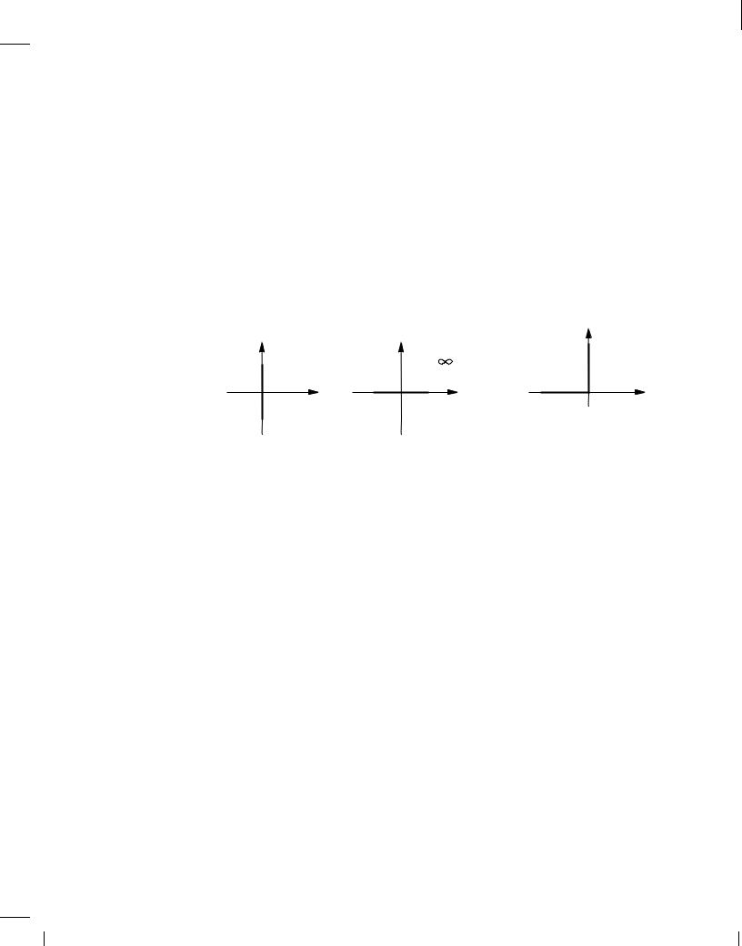
I/V Characteristics In studying electronic devices, it is often helpful to accompany equations with graphical visualizations. A common type of plot is that of the current/voltage (I/V) characteristic, i.e., the current that flows through the device as a function of the voltage across it.
Since an ideal diode behaves as a short or an open, we first construct the I/V characteristics for two special cases of Ohm's law:
R = 0 ) I = V |
= 1 |
(3.1) |
R |
|
|
R = 1 ) I = V |
= 0: |
(3.2) |
R |
|
|
The results are illustrated in Fig. 3.5(a). For an ideal diode, we combine the positive-voltage region of the first with the negative-voltage region of the second, arriving at the ID=VD characteristic in Fig. 3.5(b). Here, VD = Vanode , Vcathode, and ID is defined as the current flowing into the anode and out of the cathode.
I |
I |
|
I D |
|
Reverse |
Forward |
|||
|
R = |
|||
R = 0 |
Bias |
Bias |
||
|
||||
V |
|
V |
VD |
|
(a) |
|
|
(b) |
Figure 3.5 I/V characteristics of (a) zero and infinite resistors, (b) ideal diode.
Example 3.2
We said that an ideal diode turns on for positive anode-cathode voltages. But the characteristic in Fig. 3.5(b) does not appear to show any ID values for VD > 0. How do we interpret this plot?
Solution
This characteristic indicates that as VD exceeds zero by a very small amount, then the diode turns on and conducts infinite current if the circuit surrounding the diode can provide such a current. Thus, in circuits containing only finite currents, a forward-biased ideal diode sustains a zero voltage—similar to a short circuit.
Exercise
How is the characteristic modified if we place a 1- resistor in series with the diode?
Example 3.3
Plot the I/V characteristic for the “antiparallel” diodes shown in Fig. 3.6(a).
Solution
If VA > 0, D1 is on and D2 is off, yielding IA = 1. If VA < 0, D1 is off, but D2 is on, again leading to IA = 1. The result is illustrated in Fig. 3.6(b). The antiparallel combination therefore acts as a short for all voltages. Seemingly a useless circuit, this topology becomes much more interesting with actual diodes (Section 3.5.3).

BR |
Wiley/Razavi/Fundamentals of Microelectronics [Razavi.cls v. 2006] |
June 30, 2007 at 13:42 |
65 (1) |
|
|
|
|
Sec. 3.1 |
Ideal Diode |
|
65 |
|
|
I A |
I A |
|
VA |
D1 |
D2 |
|
|
|
VA |
|
|
(a) |
(b) |
Figure 3.6 (a) Antiparallel diodes, (b) resulting I/V characteristic.
Exercise
Repeat the above example if a 1-V battery is placed is series with the parallel combination of the diodes.
Example 3.4
Plot the I/V characteristic for the diode-resistor combination of Fig. 3.7(a).
|
I A |
|
|
|
|
|
|
|
D1 |
I A |
I A |
|
|
|
|
V |
D1 |
R 1 |
R |
1 |
R 1 |
||
|
A |
|
R 1 |
D1 |
|
||
|
R |
1 |
|
|
|
||
|
|
|
|
|
|
|
|
|
(a) |
|
|
(b) |
(c) |
|
|
|
|
|
I A |
|
I A |
|
|
|
|
|
|
|
|
|
|
|
|
|
1 |
VA |
D1 |
|
|
|
|
|
R 1 |
R 1 |
|
|
|
|
|
|
|
VA |
(e) |
|
|
|
|
|
(d) |
|
|
|
|
|
|
|
|
|
|
|
|
Figure 3.7 (a) Diode-resistor series combination, (b) equivalent circuit under forward bias, (c) equivalent circuit under reverse bias, (d) I/V characteristic, (e) equivalent circuit if D1 is on.
Solution
We surmise that, if VA > 0, the diode is on [Fig. 3.7(b)] and IA = VA=R1 because VD1 = 0 for an ideal diode. On the other hand, if VA < 0, D1 is probably off [Fig. 3.7(c)] and ID = 0. Figure 3.7(d) plots the resulting I/V characteristic.
The above observations are based on guesswork. Let us study the circuit more rigorously. We begin with VA < 0, postulating that the diode is off. To confirm the validity of this guess, let us assume D1 is on and see if we reach a conflicting result. If D1 is on, the circuit is reduced to that in Fig. 3.7(e), and if VA is negative, so is IA; i.e., the actual current flows from right to left. But this implies that D1 carries a current from its cathode to its anode, violating the definition of the diode. Thus, for VA < 0, D1 remains off and IA = 0.
As VA rises above zero, it tends to forward bias the diode. Does D1 turn on for any VA > 0 or does R1 shift the turn-on point? We again invoke proof by contradiction. Suppose for some

BR |
Wiley/Razavi/Fundamentals of Microelectronics [Razavi.cls v. 2006] |
June 30, 2007 at 13:42 |
66 (1) |
|
|
|
|
66 |
Chap. 3 |
Diode Models and Circuits |
VA > 0, D1 is still off, behaving as an open circuit and yielding IA = 0. The voltage drop across R1 is therefore equal to zero, suggesting that VD1 = VA and hence ID1 = 1 and contradicting the original assumption. In other words, D1 turns on for any VA > 0.
Exercise
Repeat the above analysis if the terminals of the diode are swapped.
The above example leads to two important points. First, the series combination of D1 and R1 acts as an open for negative voltages and as a resistor of value R1 for positive voltages. Second, in the analysis of circuits, we can assume an arbitrary state (on or off) for each diode and proceed with the computation of voltages and currents; if the assumptions are incorrect, the final result contradicts the original assumptions. Of course, it is helpful to first examine the circuit carefully and make an intuitive guess.
Example 3.5
Why are we interested in I/V characteristics rather than V/I characteristics?
Solution
In the analysis of circuits, we often prefer to consider the voltage to be the “cause” and the current, the “effect.” This is because in typical circuits, voltage polarities can be predicted more readily and intuitively than current polarities. Also, devices such as transistors fundamentally produce current in response to voltage.
Exercise
Plot the V/I characteristic of an ideal diode.
Example 3.6
In the circuit of Fig. 3.8, each input can assume a value of either zero or +3 V. Determine the response observed at the output.
D 1
VA

VB


 Vout
Vout
D 2
RL
Figure 3.8 OR gate realized by diodes.
Solution
If VA = +3 V, and VB = 0, then we surmise that D1 is forward-biased and D2, reverse-biased. Thus, Vout = VA = +3 V. If uncertain, we can assume both D1 and D2 are forward-biased, immediately facing a conflict: D1 enforces a voltage of +3 V at the output whereas D2 shorts Vout to VB = 0. This assumption is therefore incorrect.

BR |
Wiley/Razavi/Fundamentals of Microelectronics [Razavi.cls v. 2006] |
June 30, 2007 at 13:42 |
67 (1) |
|
|
|
|
Sec. 3.1 |
Ideal Diode |
67 |
The symmetry of the circuit with respect to VA and VB suggests that Vout = VB = +3 V if VA = 0 and VB = +3 V. The circuit operates as a logical OR gate and was in fact used in early digital computers.
Exercise
Construct a three-input OR gate.
Example 3.7
Is an ideal diode on or off if VD = 0?
Solution
An ideal diode experiencing a zero voltage must carry a zero current (why?). However, this does not mean it acts as an open circuit. After all, a piece of wire experiencing a zero voltage behaves similarly. Thus, the state of an ideal diode with VD = 0 is somewhat arbitrary and ambiguous. In practice, we consider slightly positive or negative voltages to determine the response of a diode circuit.
Exercise
Repeat the above example if a 1- resistor is placed in series with the diode.
Input/Output Characteristics Electronic circuits process an input and generate a corresponding output. It is therefore instructive to construct the input/output characteristics of a circuit by varying the input across an allowable range and plotting the resulting output.
An example, consider the circuit depicted in Fig. 3.9(a), where the output is defined as the voltage across D1. If Vin < 0, D1 is reverse biased, reducing the circuit to that in Fig. 3.9(b). Since no current flows through R1, we have Vout = Vin. If Vin > 0, then D1 is forward biased, shorting the output and forcing Vout = 0 [Fig. 3.9(c)]. Figure 3.9(d) illustrates the overall input/output characteristic.
3.1.3 Application Examples
Recall from Fig. 3.2 that we arrived at the concept of the ideal diode as a means of converting x(t) to y(t). Let us now design a circuit that performs this function. We may naturally construct the circuit as shown in Fig. 3.10(a). Unfortunately, however, the cathode of the diode is “floating,” the output current is always equal to zero, and the state of the diode is ambiguous. We therefore modify the circuit as depicted in Fig. 3.10(b) and analyze its response to a sinusoidal input [Fig. 3.10(c)]. Since R1 has a tendency to maintain the cathode of D1 near zero, as Vin rises, D1 is forward biased, shorting the output to the input. This state holds for the positive half cycle. When Vin falls below zero, D1 turns off and R1 ensures that Vout = 0 because IDR1 = 0.5 The circuit of Fig. 3.10(b) is called a “rectifier.”
It is instructive to plot the input/output characteristic of the circuit as well. Noting that if Vin < 0, D1 is off and Vout = 0, and if Vin > 0, D1 is on and Vout = Vin, we obtain the
5Note that without R1, the output voltage is not defined because a floating node can assume any potential.

BR |
Wiley/Razavi/Fundamentals of Microelectronics [Razavi.cls v. 2006] |
June 30, 2007 at 13:42 |
68 (1) |
|
|
|
|
68 |
|
|
|
Chap. 3 |
Diode Models and Circuits |
|
|
|
|
Vin < 0 |
|
|
Vin > 0 |
|
R1 |
|
R1 |
|
|
R1 |
Vin |
D1 |
Vout |
Vin |
Vout |
Vin |
Vout |
|
(a) |
|
(b) |
|
|
(c) |
|
|
|
Vout |
|
|
|
Vin
1
(d)
Figure 3.9 (a) Resistor-diode circuit, (b) equivalent circuit for negative input, (c) equivalent circuit for positive input, (d) input/output characteristic.
behavior shown in Fig. 3.10(d). The rectifier is a nonlinear circuit because if Vin ! ,Vin then
Vout 6! ,Vout.
Example 3.8
Is it a coincidence that the characteristics in Figs. 3.7(d) and 3.10(d) look similar?
Solution
No, we recognize that the output voltage in Fig. 3.10(b) is simply equal to IAR1 in Fig. 3.7(a). Thus, the two plots differ by only a scaling factor equal to R1.
Exercise
Construct the characteristic if the terminals of D1 are swapped.
We now determine the time average (dc value) of the output waveform in Fig. 3.10(c) to arrive at another interesting application. Suppose Vin = Vp sin !t, where ! = 2 =T denotes the frequency in radians per second and T the period. Then, in the first cycle after t = 0, we have
V = V |
p |
sin !t for 0 t T |
(3.3) |
||
out |
|
|
2 |
|
|
|
|
|
|
|
|
= 0 |
|
for |
T |
t T |
(3.4) |
|
|
|
2 |
|
|
To compute the average, we obtain the area under Vout and normalize the result to the period:
Vout;avg = T1 Z
= T1 Z
T |
|
Vout(t)dt |
(3.5) |
0 |
|
T=2 |
|
Vp sin !tdt |
(3.6) |
0 |
|

BR |
Wiley/Razavi/Fundamentals of Microelectronics [Razavi.cls v. 2006] |
June 30, 2007 at 13:42 |
69 (1) |
|
|
|
|
Sec. 3.1 |
Ideal Diode |
|
|
|
|
|
69 |
|
|
|
|
D 1 |
|
|
|
D 1 |
|
|
|
Vin |
|
|
Vout |
Vin |
R 1 |
Vout |
|
|
|
(a) |
|
|
|
(b) |
|
|
|
Vin |
|
|
|
|
|
|
|
|
|
|
|
|
t |
Vout |
|
|
|
|
|
|
|
|
|
|
|
Vin |
R 1 |
Vin |
|
R 1 |
|
|
1 |
|
|
|
|
Vin |
||||
|
|
|
|
|
|
|
|
|
|
|
Vout |
|
|
|
Rectified |
|
|
|
|
|
|
|
Half Cycles |
|
|
|
|
|
0 |
T |
T |
3T |
2T t |
|
|
|
|
|
2 |
|
2 |
|
|
|
(d)
(c)
Figure 3.10 (a) A diode operating as a rectifier, (b) complete rectifier, (c) input and output waveforms, (d) input/output characteristic.
= |
1 |
|
|
Vp |
[, cos !t]T=2 |
(3.7) |
|
|
|
||||
|
T |
|
! |
0 |
|
|
|
|
|
|
|||
= |
Vp |
: |
|
|
(3.8) |
|
|
|
|
||||
|
|
|
|
|
||
Thus, the average is proportional to Vp, an expected result because a larger input amplitude yields a greater area under the rectified half cycles.
The above observation reveals that the average value of a rectified output can serve as a measure of the “strength” (amplitude) of the input. That is, a rectifier can operate as a “signal strength indicator.” For example, since cellphones receive varying levels of signal depending on the user's location and environment, they require an indicator to determine how much the signal must be amplified.
Example 3.9
A cellphone receives a 1.8-GHz signal with a peak amplitude ranging from 2 V to 10 mV. If the signal is applied to a rectifier, what is the corresponding range of the output average?
Solution
The rectified output exhibits an average value ranging from 2 V=( ) = 0:637 V to 10 mV/( ) = 3:18 mV.
Exercise
Do the above results change if a 1- resistor is placed in series with the diode?

BR |
Wiley/Razavi/Fundamentals of Microelectronics [Razavi.cls v. 2006] |
June 30, 2007 at 13:42 |
70 (1) |
|
|
|
|
70 |
Chap. 3 |
Diode Models and Circuits |
In our effort toward understanding the role of diodes, we examine another circuit that will eventually (in Section 3.5.3) lead to some important applications. First, consider the topology in Fig. 3.11(a), where a 1-V battery is placed in series with an ideal diode. How does this circuit behave? If V1 < 0, the cathode voltage is higher than the anode voltage, placing D1 in reverse bias. Even if V1 is slightly greater than zero, e.g., equal to 0.9 V, the anode is not positive enough to forward bias D1. Thus, V1 must approach +1 V for D1 to turn on. Shown in Fig. 3.11(a), the I/V characteristic of the diode-battery combination resembles that of a diode, but shifted to the right by 1 V.
|
|
|
I 1 |
|
|
|
|
|
|
I 1 |
|
|
|
V1 |
D1 |
|
|
|
|
VB |
|
|
|
|
|
|
1 V |
|
|
|
|
|
|
+1 V |
V1 |
|
|
|
|
(a) |
|
|
|
|
Vin |
|
Vout |
|
R1 |
|
|
|
|
Vin |
D1 |
Vout |
|
t |
|
V |
|
Vin |
|||
|
|
|
out |
|
1 |
|
|
|
|
|
|
|
|
|
|
t |
|
|
|
|
|
(b) |
|
R1 |
|
|
Vin |
+ Vp |
|
|
|
|
Vout |
||
|
|
|
|
t |
|
D1 |
|
|
|
|
|
|
|
|
− Vp |
+1 V |
|
Vin |
|
Vout |
|
||
VB |
1 V |
Vout |
+ 1 V |
|
|
|
+1 V Vin |
||||
|
|
|
|||
|
|
|
|
t |
1 |
|
|
|
|
|
− Vp
(c)
Figure 3.11 (a) Diode-battery circuit, (b) resistor-diode circuit, (c) addition of series battery to (b).
Now, let us examine the circuit in Fig. 3.11(b). Here, for Vin < 0, D1 remains off, yielding Vout = Vin. For Vin > 0, D1 acts a short, and Vout = 0. The circuit therefore does not allow the output to exceed zero, as illustrated in the output waveform and the input/output characteristic. But suppose we seek a circuit that must not allow the output to exceed +1 V (rather than zero). How should the circuit of Fig. 3.11(b) be modified? In this case, D1 must turn on only when Vout approaches +1 V, implying that a 1-V battery must be inserted in series with the diode. Depicted in Fig. 3.11(c), the modification indeed guarantees Vout +1 V for any input level. We say the circuit “clips” or “limits” at +1 V. “Limiters” prove useful in many applications and are described
in Section 3.5.3.
Example 3.10
Sketch the time average of Vout in Fig. 3.11(c) for a sinusoidal input as the battery voltage, VB,