Добавил:
Upload Опубликованный материал нарушает ваши авторские права? Сообщите нам.
Вуз: Предмет: Файл:

Fundamentals of Microelectronics

.pdf
Скачиваний:
208
Добавлен:
26.03.2015
Размер:
8.53 Mб
Скачать

BR

Wiley/Razavi/Fundamentals of Microelectronics [Razavi.cls v. 2006]

June 30, 2007 at 13:42

831 (1)


Sec. A.3

Element Descriptions


831


VDD

= 1.8 V


vdd


1 kΩ


rx


10


x


m2


0.18


5

Vout

in

m1

out


Vin


0.18

500Ω


rout


(a)


(b)


Figure A.16

.dc vin 0 1 1m

.model mymod nmos (uo=360, tox=0.4n, vth=0.5, lambda=0.4)

.end

For high-frequency analysis, we must specify the junction capacitance of the source and drain areas. As illustrated in Fig. A.17, this capacitance is partitioned into two components: the “area”

Cjsw

Cj

Figure A.17 Area and sidewall capacitances.

capacitance, Cj, and the “sidewall” capacitance, Cjsw. This separation is necessary because the values of Cj and Cjsw (e.g., per unit area) are typically unequal.

In SPICE, the above capacitance components are defined differently. The area capacitance is specified per unit area, e.g., Cj = 3 10,4 F=m2 (= 0:3 fF= m2), whereas the sidewall capacitance is defined per unit width, e.g., Cjsw = 4 10,10 F/m (= 0:4 fF/ m). With these specifications, SPICE simply calculates the overall junction capacitance as Cj ad + Cjsw pd. For example, with the above values of Cj and Cjsw, the drain junction capacitance of M1 in Example A.12 is equal to:

CDB1 = (3 10,12 m2) (3 10,4 F=m2) + (11:2 10,6 m) (4 10,10 F=m)(A.1)

= 5:38 fF:

(A.2)

Note that, if the area and perimeter values are absent in the netlist, SPICE may use a default value of zero, thus underestimating the capacitances in the circuit.

The source/drain junction capacitances exhibit a voltage dependence that may not follow the square-root equation associated with “abrupt” pn junctions. SPICE allows an equation of the form

C =

C0


;

(A.3)


1 + B


m


VR


BR

Wiley/Razavi/Fundamentals of Microelectronics [Razavi.cls v. 2006]

June 30, 2007 at 13:42

832 (1)


832

App. A Introduction to SPICE

where C0 denotes the value for zero voltage across the junction, and m typically falls in the range of 0.3 to 0.4. Thus for Cj and Cjsw, we specify

(cjo, mj)

and

(cjswo, mjsw)

A more complete MOS model may therefore appear as:

.model mymod nmos (level=1, uo=360, tox=0.4n, vth=0.5, lambda=0.4, +cjo=3e-4, mj=0.35, cjswo=40n, mjswo=0.3)

where the “level” denotes a certain complexity for the model. In practice, higher levels with many more parameters are used. Similarly, a PMOS model may be constructed as follows:

.model mymod2 pmos (level=1, uo=150, tox=0.4n, vth=-0.55, +lambda=0.5, cjo=3.5e-4, mj=0.35, cjswo=35n, mjswo=0.3)

A.4 Other Elements and Commands

A.4.1 Dependent Sources

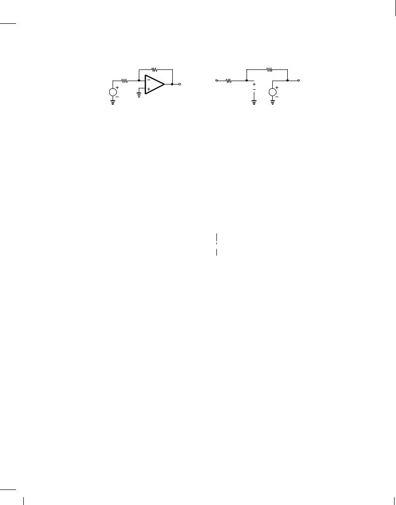
In addition to the independent voltage and current sources studied above, we may need to incorporate dependent sources in simulations. For example, as mentioned in Chapter 8, op amps can be viewed as voltage-dependent voltage sources. Similarly, a MOSFET acts as a voltage-dependent current source.

Consider the arrangement shown in Fig. A.18, where the voltage source tied between nodes C and D is equal to three times the voltage difference between nodes A and B. For simplicity,

A C

3VAB

B D

Figure A.18 Voltage-dependent voltage source.

we call (A; B) the “input nodes,” (C; D) the “output nodes,” and the factor of 3, the “gain.” Such a voltage-dependent voltage source is expressed as

Output

Input

DC

Gain

Nodes

Nodes

Value


e1 c d poly(1)

a b

0

3

Note the element name begins with the letter “e” to signify a voltage-dependent voltage source. The next two entries are the output nodes, with the first representing the positive terminal. The entry poly(1) indicates a first-order polynomial relationship between VCD and VAB. Next, the controlling (input) nodes are specified, and the zero is entered to denote a zero additional dc voltage. Finally, the gain is specified. In a more general case, this expression can realize VCD =+ VAB, where is the dc value (zero in the above example) and is the gain (3 in the above example).

Example A.13

The circuit of Fig. A.19(a) employs an op amp with a gain of 500. Construct a SPICE netlist for the circuit.

BR

Wiley/Razavi/Fundamentals of Microelectronics [Razavi.cls v. 2006]

June 30, 2007 at 13:42

833 (1)


References


833


10 k Ω


10 k Ω

1 kΩ


1 kΩ

rf


in


out

X

Vout

r1

X

Vin


eopamp


(a)


(b)

Figure A.19

Solution

We first draw and label the circuit as shown in Fig. A.19(b). Thus,

r1 in x 1k rf x out 5k

eopamp out 0 poly(1) x 0 0 -500

For the voltage-dependent current source depicted in Fig. A.20, the description is as follows:

A C

GmVAB

B D

Gm = ( 20 Ω)−1

Figure A.20 Voltage-dependent current source.

g1 c d poly(1) a b 0 0.05

where the letter g denotes a voltage-dependent current source and the gain is specified as

1=(20 ) = 0:05 ,1.

Current-controlled voltage and current sources are also described in a similar manner, but they are rarely used.

A.4.2 Initial Conditions

In the transient analysis of circuits, we may wish to specify an initial voltage at a node with respect to ground. This is accomplished using the .ic command:

.ic v(x)=0.5

This example sets the initial voltage at node X to 0.5 V.

References

1. G. Roberts and A. S. Sedra, SPICE, Oxford University Press, 1997.

Соседние файлы в предмете [НЕСОРТИРОВАННОЕ]