

Fundamentals of Microelectronics
.pdfBR |
Wiley/Razavi/Fundamentals of Microelectronics [Razavi.cls v. 2006] |
June 30, 2007 at 13:42 |
181 (1) |
|
|
|
|
Sec. 5.1 |
General Considerations |
181 |
each device. Second, we perform “small-signal analysis,” i.e., study the response of the circuit to small signals and compute quantities such as the voltage gain and I/O impedances. As an example, Fig. 5.8 illustrates the bias and signal components of a voltage and a current.
VBE |
Bias (dc) |
|
|
|
Value |
|
t |
I C |
Bias (dc) |
|
Value |
t
Figure 5.8 Bias and signal levels for a bipolar transistor.
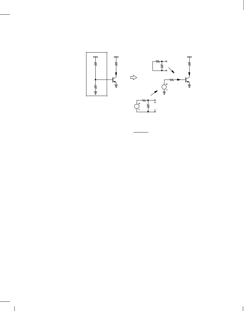
It is important to bear in mind that small-signal analysis deals with only (small) changes in voltages and currents in a circuit around their quiescent values. Thus, as mentioned in Section 4.4.4, all constant sources, i.e., voltage and current sources that do not vary with time, must be set to zero for small-signal analysis. For example, the supply voltage is constant and, while establishing proper bias points, plays no role in the response to small signals. We therefore ground all constant voltage sources4 and open all constant current sources while constructing the smallsignal equivalent circuit. From another point of view, the two steps described above follow the superposition principle: first, we determine the effect of constant voltages and currents while signal sources are set to zero, and second, we analyze the response to signal sources while constant sources are set to zero. Figure 5.9 summarizes these concepts.
DC Analysis
VCC
R C1 |
|
|
|
V |
CB |
I C1 |
I C2 |
|
|
||
VBE |
|
|
|
Small−Signal Analysis
Short |
v out |
|
v in |
Open
Figure 5.9 Steps in a general circuit analysis.
We should remark that the design of amplifiers follows a similar procedure . First, the circuitry around the transistor is designed to establish proper bias conditions and hence the necessary small-signal parameters. Second, the smallsignal behavior of the circuit is studied to verify the required performance. Some iteration between the two steps may often be necessary so as to converge toward the desired behavior.
How do we differentiate between small-signal and large-signal operations? In other words, under what conditions can we represent the devices with their small-signal models? If the signal perturbs the bias point of the device only negligibly, we say the circuit operates in the smallsignal regime. In Fig. 5.8, for example, the change in IC due to the signal must remain small. This criterion is justified because the amplifying properties of the transistor such as gm and r are
4We say all constant voltage sources are replaced by an “ac ground.”
BR |
Wiley/Razavi/Fundamentals of Microelectronics [Razavi.cls v. 2006] |
June 30, 2007 at 13:42 |
182 (1) |
|
|
|
|
182 |
Chap. 5 |
Bipolar Amplifiers |
considered constant in small-signal analysis even though they in fact vary as the signal perturbs IC. That is, a linear representation of the transistor holds only if the small-signal parameters themselves vary negligibly. The definition of “negligibly” somewhat depends on the circuit and the application, but as a rule of thumb, we consider 10% variation in the collector current as the upper bound for small-signal operation.
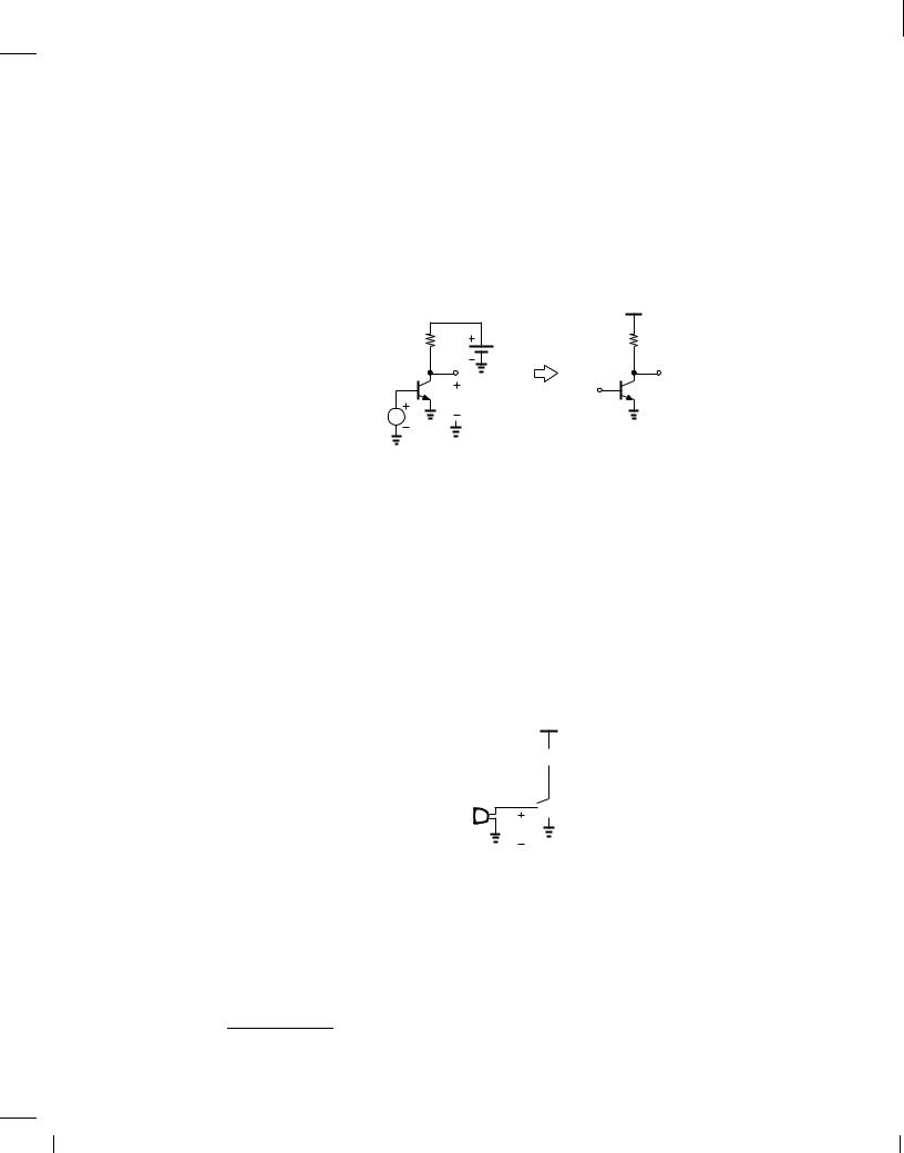
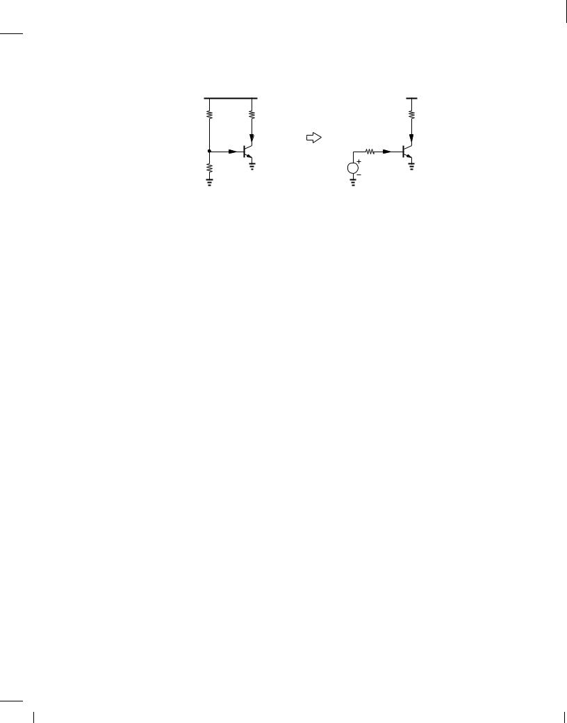
In drawing circuit diagrams hereafter, we will employ some simplified notations and symbols. Illustrated in Fig. 5.10 is an example where the battery serving as the supply voltage is replaced with a horizontal bar labeled VCC.5 Also, the input voltage source is simplified to one node called Vin, with the understanding that the other node is ground.
|
|
VCC |
R C |
VCC |
R C |
|
|
|
Q 1 |
Vin |
Vout |
|
Q 1 |
|
Vin |
Vout |
|
|
|
Figure 5.10 Notation for supply voltage.
In this chapter, we begin with the DC analysis and design of bipolar stages, developing skills to determine or create bias conditions. This phase of our study requires no knowledge of signals and hence the input and output ports of the circuit. Next, we introduce various amplifier topologies and examine their small-signal behavior.
5.2 Operating Point Analysis and Design
It is instructive to begin our treatment of operating points with an example.
Example 5.5
A student familiar with bipolar devices constructs the circuit shown in Fig. 5.11 and attempts to amplify the signal produced by a microphone. If IS = 6 10,16 A and the peak value of the microphone signal is 20 mV, determine the peak value of the output signal.
VCC
R C  1 kΩ
1 kΩ

 Vout
Vout

 Q 1
Q 1
Vin
Figure 5.11 Amplifier driven directly by a microphone.
Solution
Unfortunately, the student has forgotten to bias the transistor. (The microphone does not produce a dc output). If Vin (= VBE) reaches 20 mV, then
I |
C |
= I exp VBE |
(5.10) |
|
|
S |
VT |
|
|
|
|
|
|
|
5The subscript CC indicates supply voltage feeding the collector.
BR |
Wiley/Razavi/Fundamentals of Microelectronics [Razavi.cls v. 2006] |
June 30, 2007 at 13:42 |
183 (1) |
|
|
|
|
Sec. 5.2 |
Operating Point Analysis and Design |
183 |
|
= 1:29 10,15 A: |
(5.11) |
This change in the collector current yields a change in the output voltage equal to |
|
|
|
RC IC = 1:29 10,12 V: |
(5.12) |
The circuit generates virtually no output because the bias current (in the absence of the microphone signal) is zero and so is the transconductance.
Exercise
Repeat the above example if a constant voltage of 0.65 V is placed in series with the microphone.
As mentioned in Section 5.1.2, biasing seeks to fulfill two objectives: ensure operation in the forward active region, and set the collector current to the value required in the application. Let us return to the above example for a moment.
Example 5.6
Having realized the bias problem, the student in Example 5.5 modifies the circuit as shown in Fig. 5.12, connecting the base to VCC to allow dc biasing for the base-emitter junction. Explain why the student needs to learn more about biasing.
VCC = 2.5 V
R C  1 kΩ
1 kΩ

 Vout
Vout

 Q 1
Q 1
Figure 5.12 Amplifier with base tied to VCC.
Solution
The fundamental issue here is that the signal generated by the microphone is shorted to VCC. Acting as an ideal voltage source, VCC maintains the base voltage at a constant value, prohibiting any change introduced by the microphone. Since VBE remains constant, so does Vout, leading to no amplification.
Another important issue relates to the value of VBE: with VBE = VCC = 2:5 V, enormous currents flow into the transistor.
Exercise
Does the circuit operate better if a resistor is placed in series with the emitter of Q1?
BR |
Wiley/Razavi/Fundamentals of Microelectronics [Razavi.cls v. 2006] |
June 30, 2007 at 13:42 |
184 (1) |
|
|
|
|
184 |
Chap. 5 |
Bipolar Amplifiers |
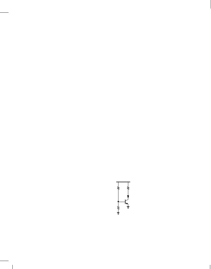
5.2.1 Simple Biasing
Now consider the topology shown in Fig. 5.13, where the base is tied to VCC through a relatively large resistor, RB, so as to forward-bias the base-emitter junction. Our objective is to determine the terminal voltages and currents of Q1 and obtain the conditions that ensure biasing in the active mode. How do we analyze this circuit? One can replace Q1 with its large-signal model and apply KVL and KCL, but the resulting nonlinear equation(s) yield little intuition. Instead, we recall that the base-emitter voltage in most cases falls in the range of 700 to 800 mV and can be considered relatively constant. Since the voltage drop across RB is equal to RBIB, we have
|
VCC |
R B |
RC |
|
Y |
|
I C |
|
X |
I B |
Q 1 |
|
Figure 5.13 Use of base resistance for base current path.
RBIB + VBE = VCC
and hence
IB = VCC , VBE :
RB
With the base current known, we write
IC = VCC , VBE ;
RB
note that the voltage drop across RC is equal to RC IC, and hence obtain VCE as
VCE = VCC , RCIC
= VCC , VCC , VBE RC:
RB
(5.13)
(5.14)
(5.15)
(5.16)
(5.17)
Calculation of VCE is necessary as it reveals whether the device operates in the active mode or not. For example, to avoid saturation completely, we require the collector voltage to remain above the base voltage:
V |
, VCC , VBE R > V |
BE |
: |
(5.18) |
CC |
C |
|
|
|
|
RB |
|
|
|
The circuit parameters can therefore be chosen so as to guarantee this condition.
In summary, using the sequence IB ! IC ! VCE, we have computed the important terminal currents and voltages of Q1. While not particularly interesting here, the emitter current is simply equal to IC + IB.
The reader may wonder about the error in the above calculations due to the assumption of a constant VBE in the range of 700 to 800 mV. An example clarifies this issue.
BR |
Wiley/Razavi/Fundamentals of Microelectronics [Razavi.cls v. 2006] |
June 30, 2007 at 13:42 |
185 (1) |
|
|
|
|
Sec. 5.2 |
Operating Point Analysis and Design |
185 |
Example 5.7
For the circuit shown in Fig. 5.14, determine the collector bias current. Assume = 100 and IS = 10,17 A. Verify that Q1 operates in the forward active region.
VCC = 2.5 V
100 k Ω RB R C  1 kΩ
1 kΩ
Y
 I C
I C
X
I B 
 Q 1
Q 1
Figure 5.14 Simple biased stage.
Solution
Since IS is relatively small, we surmise that the base-emitter voltage required to carry typical current level is relatively large. Thus, we use VBE = 800 mV as an initial guess and write Eq. (5.14) as
IB = |
VCC |
, VBE |
(5.19) |
|
|
|
RB |
|
|
17 A: |
(5.20) |
|||
It follows that |
|
|
|
|
IC = 1:7 mA: |
(5.21) |
|||
With this result for IC, we calculate a new value for VBE: |
|
|||
V |
= V |
T |
ln IC |
(5.22) |
BE |
|
IS |
|
|
|
|
|
|
|
|
= 852 mV; |
(5.23) |
||
and iterate to obtain more accurate results. That is,
IB = |
VCC , VBE |
(5.24) |
|
RB |
|
= |
16:5 A |
(5.25) |
and hence
IC = 1:65 mA: |
(5.26) |
Since the values given by (5.21) and (5.26) are quite close, we consider IC = 1:65 mA accurate enough and iterate no more.
Writing (5.16), we have
VCE = VCC , RCIC |
(5.27) |
= 0:85 V; |
(5.28) |
BR |
Wiley/Razavi/Fundamentals of Microelectronics [Razavi.cls v. 2006] |
June 30, 2007 at 13:42 |
186 (1) |
|
|
|
|
186 |
Chap. 5 |
Bipolar Amplifiers |
a value nearly equal to VBE. The transistor therefore operates near the edge of active and saturation modes.
Exercise
What value of RB provides a reverse bias of 200 mV across the base-collector junction?
The biasing scheme of Fig. 5.13 merits a few remarks. First, the effect of VBE “uncertainty” becomes more pronounced at low values of VCC because VCC ,VBE determines the base current. Thus, in low-voltage design—an increasingly common paradigm in modern electronic systems— the bias is more sensitive to VBE variations among transistors or with temperature . Second, we recognize from Eq. (5.15) that IC heavily depends on , a parameter that may change considerably. In the above example, if increases from 100 to 120, then IC rises to 1.98 mA and VCE falls to 0.52, driving the transistor toward heavy saturation. For these reasons, the topology of Fig. 5.13 is rarely used in practice.
5.2.2 Resistive Divider Biasing
In order to suppress the dependence of IC upon , we return to the fundamental relationship IC = IS exp(VBE =VT ) and postulate that IC must be set by applying a well-defined VBE. Figure 5.15 depicts an example, where R1 and R2 act as a voltage divider, providing a baseemitter voltage equal to
|
|
|
|
R2 |
|
(5.29) |
||
|
|
VX = |
|
VCC; |
||||
|
|
R1 + R2 |
||||||
if the base current is negligible. Thus, |
|
|
|
|
|
|||
I |
C |
= I exp |
|
R2 |
VCC ; |
(5.30) |
||
|
|
|
||||||
|
S |
R1 |
+ R2 |
VT |
|
|||
|
|
|
|
|
||||
a quantity independent of . Nonetheless, the design must ensure that the base current remains negligible.
|
VCC |
R 1 |
RC |
|
Y |
|
I C |
|
X |
|
Q 1 |
R 2 |
|
Figure 5.15 Use of resistive divider to define VBE.
Example 5.8
Determine the collector current of Q1 in Fig. 5.16 if IS = 10,17 A and = 100. Verify that the base current is negligible and the transistor operates in the active mode.
BR |
Wiley/Razavi/Fundamentals of Microelectronics [Razavi.cls v. 2006] |
June 30, 2007 at 13:42 |
187 (1) |
|
|
|
|
Sec. 5.2 |
Operating Point Analysis and Design |
|
|
|
|
|
187 |
|||||||||||
|
|
|
|
|
|
|
|
|
|
|
|
|
|
|
|
|
|
VCC = 2.5 V |
|
|
|
|
|
|
|
|
|
|
|
|
|
|
|
|
|
|
|
|
17 k Ω |
|
|
|
R1 |
R C |
|
|
|
|
5 kΩ |
|||||||
|
|
|
|
|
||||||||||||||
|
|
|
|
|
||||||||||||||
|
|
|
|
|
|
|
|
|
|
Y |
|
|
|
I C |
||||
|
|
|
|
|
|
|
|
|
X |
|
|
|
|
|
|
|
||
|
8 k Ω |
|
|
|
|
|
|
|
|
|
|
Q 1 |
||||||
|
|
|
|
|
|
|
||||||||||||
|
|
|
|
R2 |
|
|
|
|
|
|
||||||||
|
|
|
|
|
|
|
|
|
|
|
|
|
|
|||||
|
|
|
|
|
|
|
|
|
|
|
|
|
|
|||||
|
|
|
|
|
|
|
|
|
|
|
||||||||
|
|
|
|
|
|
|
|
|
|
|
||||||||
|
|
|
|
|
|
|
|
|
|
|
|
|
|
|||||
|
|
|
|
|
|
|
|
|
|
|
|
|
|
|
|
|||
Figure 5.16 Example of biased stage. |
|
|
|
|
|
|
|
|
|
|
|
|
|
|
||||
Solution
Neglecting the base current of Q1, we have
VX = |
|
R2 |
VCC |
(5.31) |
R1 |
+ R2 |
|||
= 800 mV: |
|
(5.32) |
||
It follows that |
|
|
|
|
IC = IS exp VBE |
(5.33) |
|||
|
|
VT |
|
|
= 231 A |
|
(5.34) |
||
and |
|
|
|
|
IB = 2:31 A: |
(5.35) |
|||
Is the base current negligible? With which quantity should this value be compared? Provided by the resistive divider, IB must be negligible with respect to the current flowing through R1 and
R2:
? |
VCC |
|
(5.36) |
|
IB |
: |
|||
|
||||
|
R1 + R2 |
|
||
This condition indeed holds in this example because VCC =(R1 + R2) = 100 A 43IB. |
||||
We also note that |
|
|
|
|
VCE = 1:345 V; |
(5.37) |
|||
and hence Q1 operates in the active region. |
|
|
|
|
Exercise
What is the maximum value of RC if Q1 must remain in soft saturation?
The analysis approach taken in the above example assumes a negligible base current, requiring verification at the end. But what if the end result indicates that IB is not negligible? We now analyze the circuit without this assumption. Let us replace the voltage divider with a Thevenin
BR |
Wiley/Razavi/Fundamentals of Microelectronics [Razavi.cls v. 2006] |
June 30, 2007 at 13:42 |
188 (1) |
|
|
|
|
188 |
|
Chap. 5 |
Bipolar Amplifiers |
equivalent (Fig. 5.17); noting that VT hev is equal to the open-circuit output voltage (VX when |
|||
the amplifier is disconnected): |
|
|
|
VCC |
VCC |
R1 |
VCC |
R 1 |
RC |
R 2 |
RC |
|
|
|
|
I C |
I C |
X |
RThev X |
Q 1 |
Q 1 |
|
I B |
R 2 |
VThev |
R1
VCC R 2 VThev
Figure 5.17 Use of Thevenin equivalent to calculate bias.
R2 |
(5.38) |
VT hev = R1 + R2 VCC: |
Moreover, RT hev is given by the output resistance of the network if VCC is set to zero:
|
|
RT hev = R1jjR2: |
|
(5.39) |
|
The simplified circuit yields: |
|
|
|
|
|
|
|
VX = VT hev , IBRT hev |
|
(5.40) |
|
and |
|
|
|
|
|
I |
C |
= I exp VT hev |
, IB RT hev |
: |
(5.41) |
|
S |
VT |
|
|
|
|
|
|
|
|
|
This result along with IC = IB forms the system of equations leading to the values of IC and IB. As in the previous examples, iterations prove useful here, but the exponential dependence in Eq. (5.41) gives rise to wide fluctuations in the intermediate solutions. For this reason, we rewrite (5.41) as
I = V |
|
, V |
|
ln IC |
|
1 |
; |
(5.42) |
T hev |
T |
|
||||||
B |
|
IS |
|
RT hev |
|
|||
|
|
|
|
|
|
|||
and begin with a guess for VBE = VT ln(IC =IS). The iteration then follows the sequence
VBE ! IB ! IC ! VBE ! .
Example 5.9
Calculate the collector current of Q1 in Fig. 5.18(a). Assume = 100 and IS = 10,17 A.
Solution
Constructing the equivalent circuit shown in Fig. 5.18(b), we note that
VT hev = |
|
R2 |
VCC |
(5.43) |
R1 |
+ R2 |
BR |
Wiley/Razavi/Fundamentals of Microelectronics [Razavi.cls v. 2006] |
June 30, 2007 at 13:42 |
189 (1) |
|
|
|
|
Sec. 5.2 Operating Point Analysis and Design |
189 |
||
|
|
VCC = 2.5 V |
VCC |
170 k Ω |
R1 |
R C 5 kΩ |
RC |
|
|
Y |
|
|
|
I C |
I C |
|
X |
Q 1 |
RThev X |
|
|
Q 1 |
|
80 k Ω |
|
I B |
I B |
R2 |
|
VThev |
|
Figure 5.18 (a) Stage with resistive divider bias, (b) stage with Thevenin equivalent for the resistive divider and VCC.
= 800 mV |
(5.44) |
and
RT hev = R1jjR2 |
(5.45) |
= 54:4 k : |
(5.46) |
We begin the iteration with an initial guess VBE = 750 mV (because we know that the voltage drop across RT hev makes VBE less than VT hev), thereby arriving at the base current:
IB = |
VT hev , VBE |
(5.47) |
|
RT hev |
|
= |
0:919 A: |
(5.48) |
Thus, IC = IB = 91:9 A and
V |
= V |
T |
ln IC |
(5.49) |
BE |
|
IS |
|
|
|
|
|
|
|
|
= 776 mV: |
(5.50) |
||
It follows that IB = 0:441 A and hence IC = 44:1 A, still a large fluctuation with respect to the first value from above. Continuing the iteration, we obtain VBE = 757 mV, IB = 0:79 A and IC = 79:0 A. After many iterations, VBE 766 mV and IC = 63 A.
Exercise
How much can R2 be increased if Q1 must remain in soft saturation?
While proper choice of R1 and R2 in the topology of Fig. 5.15 makes the bias relatively insensitive to , the exponential dependence of IC upon the voltage generated by the resistive divider still leads to substantial bias variations. For example, if R2 is 1% higher than its nominal value, so is VX , thus multiplying the collector current by exp(0:01VBE=VT ) 1:36 (for VBE = 800 mV). In other words, a 1% error in one resistor value introduces a 36% error in the collector current. The circuit is therefore still of little practical value.
BR |
Wiley/Razavi/Fundamentals of Microelectronics [Razavi.cls v. 2006] |
June 30, 2007 at 13:42 |
190 (1) |
|
|
|
|
190 |
Chap. 5 |
Bipolar Amplifiers |
5.2.3 Biasing with Emitter Degeneration
A biasing configuration that alleviates the problem of sensitivity to and VBE is shown in Fig. 5.19. Here, resistor RE appears in series with the emitter, thereby lowering the sensitivity to VBE. From an intuitive viewpoint, this occurs because RE exhibits a linear (rather than exponential) I- V relationship. Thus, an error in VX due to inaccuracies in R1, R2, or VCC is partly “absorbed” by RE, introducing a smaller error in VBE and hence IC. Called “emitter degeneration,” the
|
VCC |
R 1 |
RC |
|
Y |
|
I C |
|
X |
|
Q 1 |
R 2 |
P |
I E |
RE
Figure 5.19 Addition of degeneration resistor to stabilize bias point.
addition of RE in series with the emitter alters many attributes of the circuit, as described later in this chapter.
To understand the above property, let us determine the bias currents of the transistor. Neglecting the base current, we have VX = VCCR2=(R1 + R2). Also, VP = VX , VBE, yielding
I = |
VP |
|
|
|
|
(5.51) |
|
|
|
|
|||
E |
RE |
|
|
|
|
|
|
|
|
|
|
||
= |
1 |
V |
|
R2 |
, V |
(5.52) |
|
CC R1 + R2 |
|||||
|
RE |
BE |
|
|||
IC ; |
|
|
|
(5.53) |
||
if 1. How can this result be made less sensitive to VX or VBE variations? If the voltage drop across RE, i.e., the difference between VCCR2=(R1 + R2) and VBE is large enough to absorb and swamp such variations, then IE and IC remain relatively constant. An example illustrates this point.
Example 5.10
Calculate the bias currents in the circuit of Fig. 5.20 and verify that Q1 operates in the forward active region. Assume = 100 and IS = 5 10,17 A. How much does the collector current change if R2 is 1% higher than its nominal value?
Solution
We neglect the base current and write
VX = VCC |
R2 |
(5.54) |
R1 + R2 |
||
= 900 mV: |
(5.55) |
|
Using VBE = 800 mV as an initial guess, we have |
|
|
VP = VX , VBE |
(5.56) |
|
= 100 mV; |
(5.57) |
|