- •Data Manual
- •Release History
- •Contents
- •List of Figures
- •List of Tables
- •1 Features
- •1.1 KeyStone Architecture
- •1.2 Device Description
- •1.3 Functional Block Diagram
- •2 Device Overview
- •2.1 Device Characteristics
- •2.2 DSP Core Description
- •2.3 Memory Map Summary
- •2.4 Boot Sequence
- •2.5 Boot Modes Supported and PLL Settings
- •2.5.1 Boot Device Field
- •2.5.2 Device Configuration Field
- •2.5.2.1 Sleep / EMIF16 Boot Device Configuration
- •2.5.2.2 Ethernet (SGMII) Boot Device Configuration
- •2.5.2.3 Serial Rapid I/O Boot Device Configuration
- •2.5.2.4 PCI Boot Device Configuration
- •2.5.2.5 I2C Boot Device Configuration
- •2.5.2.6 SPI Boot Device Configuration
- •2.5.2.7 HyperLink Boot Device Configuration
- •2.5.3 PLL Boot Configuration Settings
- •2.6 Second-Level Bootloaders
- •2.7 Terminals
- •2.8 Terminal Functions
- •2.9 Development
- •2.9.1 Development Support
- •2.9.2 Device Support
- •2.9.2.1 Device and Development-Support Tool Nomenclature
- •Related Documentation from Texas Instruments
- •3 Device Configuration
- •3.1 Device Configuration at Device Reset
- •3.2 Peripheral Selection After Device Reset
- •3.3 Device State Control Registers
- •3.3.1 Device Status Register
- •3.3.2 Device Configuration Register
- •3.3.3 JTAG ID (JTAGID) Register Description
- •3.3.4 Kicker Mechanism (KICK0 and KICK1) Register
- •3.3.5 LRESETNMI PIN Status (LRSTNMIPINSTAT) Register
- •3.3.6 LRESETNMI PIN Status Clear (LRSTNMIPINSTAT_CLR) Register
- •3.3.7 Reset Status (RESET_STAT) Register
- •3.3.8 Reset Status Clear (RESET_STAT_CLR) Register
- •3.3.9 Boot Complete (BOOTCOMPLETE) Register
- •3.3.10 Power State Control (PWRSTATECTL) Register
- •3.3.11 NMI Even Generation to CorePac (NMIGRx) Register
- •3.3.12 IPC Generation (IPCGRx) Registers
- •3.3.13 IPC Acknowledgement (IPCARx) Registers
- •3.3.14 IPC Generation Host (IPCGRH) Register
- •3.3.15 IPC Acknowledgement Host (IPCARH) Register
- •3.3.16 Timer Input Selection Register (TINPSEL)
- •3.3.17 Timer Output Selection Register (TOUTPSEL)
- •3.3.18 Reset Mux (RSTMUXx) Register
- •3.4 Pullup/Pulldown Resistors
- •4 System Interconnect
- •4.1 Internal Buses, Bridges, and Switch Fabrics
- •4.2 Data Switch Fabric Connections
- •4.3 Configuration Switch Fabric
- •4.4 Bus Priorities
- •5 C66x CorePac
- •5.1 Memory Architecture
- •5.1.1 L1P Memory
- •5.1.2 L1D Memory
- •5.1.3 L2 Memory
- •5.1.4 MSMC SRAM
- •5.1.5 L3 Memory
- •5.2 Memory Protection
- •5.3 Bandwidth Management
- •5.4 Power-Down Control
- •5.5 C66x CorePac Resets
- •5.6 C66x CorePac Revision
- •5.7 C66x CorePac Register Descriptions
- •6 Device Operating Conditions
- •6.1 Absolute Maximum Ratings
- •6.2 Recommended Operating Conditions
- •6.3 Electrical Characteristics
- •7 TMS320C6678 Peripheral Information and Electrical Specifications
- •7.1 Parameter Information
- •7.1.1 1.8-V Signal Transition Levels
- •7.1.2 Timing Parameters and Board Routing Analysis
- •7.2 Recommended Clock and Control Signal Transition Behavior
- •7.3 Power Supplies
- •7.3.1 Power-Supply Sequencing
- •7.3.1.1 POR-Controlled Device Initialization
- •7.3.1.2 RESETFULL-Controlled Device Initialization
- •7.3.1.3 Prolonged Resets
- •7.3.2 Power-Down Sequence
- •7.3.3 Power Supply Decoupling and Bulk Capacitors
- •7.3.4 SmartReflex
- •7.4 Enhanced Direct Memory Access (EDMA3) Controller
- •7.4.1 EDMA3 Device-Specific Information
- •7.4.2 EDMA3 Channel Synchronization Events
- •7.4.3 EDMA3 Peripheral Register Description(s)
- •7.5 Interrupts
- •7.5.1 Interrupt Sources and Interrupt Controller
- •7.5.2 INTC Registers
- •7.5.2.1 INTC0/INTC1 Register Map
- •7.5.2.2 INTC2 Register Map
- •7.5.2.3 INTC3 Register Map
- •7.5.3 Inter-Processor Register Map
- •7.5.4 External Interrupts Electrical Data/Timing
- •7.6.1 MPU Registers
- •7.6.1.1 MPU Register Map
- •7.6.1.2 Device-Specific MPU Registers
- •7.6.2 MPU Programmable Range Registers
- •7.6.2.1 Programmable Range n Start Address Register (PROGn_MPSAR)
- •7.6.2.2 Programmable Range n - End Address Register (PROGn_MPEAR)
- •7.6.2.3 Programmable Range n Memory Protection Page Attribute Register (PROGn_MPPA)
- •7.7 Reset Controller
- •7.7.1 Power-on Reset
- •7.7.2 Hard Reset
- •7.7.3 Soft Reset
- •7.7.4 Local Reset
- •7.7.5 Reset Priority
- •7.7.6 Reset Controller Register
- •7.7.7 Reset Electrical Data / Timing
- •7.8 Main PLL and PLL Controller
- •7.8.1 Main PLL Controller Device-Specific Information
- •7.8.1.1 Internal Clocks and Maximum Operating Frequencies
- •7.8.1.2 Main PLL Controller Operating Modes
- •7.8.1.3 Main PLL Stabilization, Lock, and Reset Times
- •7.8.2 PLL Controller Memory Map
- •7.8.2.1 PLL Secondary Control Register (SECCTL)
- •7.8.2.2 PLL Controller Divider Register (PLLDIV2, PLLDIV5, PLLDIV8)
- •7.8.2.3 PLL Controller Clock Align Control Register (ALNCTL)
- •7.8.2.4 PLLDIV Divider Ratio Change Status Register (DCHANGE)
- •7.8.2.5 SYSCLK Status Register (SYSTAT)
- •7.8.2.6 Reset Type Status Register (RSTYPE)
- •7.8.2.7 Reset Control Register (RSTCTRL)
- •7.8.2.8 Reset Configuration Register (RSTCFG)
- •7.8.2.9 Reset Isolation Register (RSISO)
- •7.8.3 Main PLL Control Register
- •7.8.4 Main PLL Controller/SRIO/HyperLink/PCIe Clock Input Electrical Data/Timing
- •7.9.1 DDR3 PLL Control Register
- •7.9.2 DDR3 PLL Device-Specific Information
- •7.9.3 DDR3 PLL Input Clock Electrical Data/Timing
- •7.10 PASS PLL
- •7.10.1 PASS PLL Control Register
- •7.10.2 PASS PLL Device-Specific Information
- •7.11 DDR3 Memory Controller
- •7.11.1 DDR3 Memory Controller Device-Specific Information
- •7.11.2 DDR3 Memory Controller Electrical Data/Timing
- •7.12 I2C Peripheral
- •7.12.1 I2C Device-Specific Information
- •7.12.2 I2C Peripheral Register Description(s)
- •7.12.3 I2C Electrical Data/Timing
- •7.12.3.1 Inter-Integrated Circuits (I2C) Timing
- •7.13 SPI Peripheral
- •7.13.1 SPI Electrical Data/Timing
- •7.13.1.1 SPI Timing
- •7.14 HyperLink Peripheral
- •7.15 UART Peripheral
- •7.16 PCIe Peripheral
- •7.17 TSIP Peripheral
- •7.18 EMIF16 Peripheral
- •7.19 Packet Accelerator
- •7.20 Security Accelerator
- •7.21 Ethernet MAC (EMAC)
- •7.22 Management Data Input/Output (MDIO)
- •7.23 Timers
- •7.23.1 Timers Device-Specific Information
- •7.23.2 Timers Electrical Data/Timing
- •7.24 Serial RapidIO (SRIO) Port
- •7.25 General-Purpose Input/Output (GPIO)
- •7.25.1 GPIO Device-Specific Information
- •7.25.2 GPIO Electrical Data/Timing
- •7.26 Semaphore2
- •7.27 Emulation Features and Capability
- •7.27.1 Advanced Event Triggering (AET)
- •7.27.2 Trace
- •7.27.2.1 Trace Electrical Data/Timing
- •7.27.3 IEEE 1149.1 JTAG
- •7.27.3.1 IEEE 1149.1 JTAG Compatibility Statement
- •7.27.3.2 JTAG Electrical Data/Timing
- •8 Mechanical Data
- •8.1 Thermal Data
- •8.2 Packaging Information
- •8.3 Package CYP
TMS320C6678
Multicore Fixed and Floating-Point Digital Signal Processor
www.ti.com |
SPRS691—November 2010 |
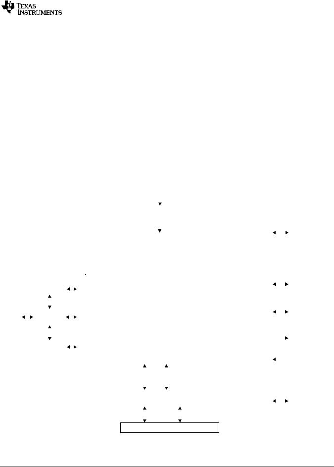
|
5 C66x CorePac
The C66x CorePac consists of several components:
•The C66x DSP and associated C66x CorePac core
•Level-one and level-two memories (L1P, L1D, L2)
•Data Trace Formatter (DTF)
•Embedded Trace Buffer (ETB)
•Interrupt controller
•Power-down controller
•External memory controller
•Extended memory controller
•A dedicated power/sleep controller (LPSC)
The C66x CorePac also provides support for memory protection, bandwidth management (for resources local to the C66x CorePac) and address extension. Figure 5-1 shows a block diagram of the C66x CorePac.
Figure 5-1 C66x CorePac Block Diagram
|
|
|
|
|
|
|
|
|
|
|
|
|
|
|
|
|
|
|
|
32KB L1P |
|
|
|
|
|
|
|
|
|
|
|
|
|
|
|
||||||||||||
|
|
|
|
|
|
|
|
|
|
|
|
|
|
|
|
|
|
|
|
|
|
|
|
|
|
|
|
|
|
|
|
|
|
|
|
|
|
|
|
|
|
|
|
|
|
|
|
|
|
|
|
|
|
|
|
|
|
|
|
|
|
|
|
|
|
|
|
|
|
|
|
|
|
|
|
|
|
|
|
|
|
|
|
|
|
|
|
|
|
|
|
|
|
|
|
|
|
|
|
|
|
|
|
|
|
|
|
|
|
|
|
|
|
|
|
|
|
|
|
|
|
|
|
|
|
|
|
|
|
|
|
|
|
|
|
|
|
|
|
|
|
|
|
|
|
|
|
|
|
|
|
|
|
|
|
|
|
Program Memory Controller (PMC) With |
|
|
MemoryExtendedMemoryUnified |
(XMC)ControllerController(UMC) |
|
|
|
|
|
||||||||||||||||||||||||
|
|
|
|
|
|
|
|
|
|
|
|
|
|
|
|
Memory Protect/Bandwidth Mgmt |
|
|
|
|
|
|
|
|
|
|
|
|
|||||||||||||||||||
|
|
|
|
|
|
|
|
|
|
|
|
|
|
|
|
|
|
|
|
|
|
|
|
|
|
|
|
|
|
|
|
|
|
|
|
|
|
|
|
|
|
|
|
|
L2 Cache/ |
||
|
|
|
GPSC |
|
|
|
|
|
|
|
|
|
.M1 |
|
|
|
|
|
.M2 |
|
|
|
ControllerExceptionandInterrupt |
|
|
|
|
|
SRAM |
||||||||||||||||||
|
|
|
|
|
|
|
|
|
|
|
|
|
|
|
|
|
|
|
C66x DSP Core |
|
|
|
|
|
|
|
|
|
|
|
|
|
|||||||||||||||
|
|
|
|
|
|
|
|
|
|
|
|
|
|
|
|
|
|
|
|
|
|
|
|
|
|
|
|
|
|
|
|
512KB |
|||||||||||||||
|
|
|
|
|
|
|
|
|
|
|
|
|
|
|
|
|
|
|
|
|
|
|
|
|
|
|
|
|
|
|
|
|
|
|
|
|
|
|
|
|
|
|
|
|
|
|
|
|
|
|
|
|
|
|
|
|
|
|
|
|
|
|
|
|
|
Instruction Fetch |
|
|
|
|
|
|
|
|
|
|
|
|
|
|
|||||||||||||||
|
|
|
|
|
|
|
|
|
|
|
|
|
|
|
|
|
|
|
|
|
|
|
|
|
|
|
|
|
|
|
|
|
|
|
|
|
|
|
|
|
|
|
|
|
|
|
|
|
|
|
|
|
|
|
|
|
|
|
|
|
|
|
|
|
16-/32-bit Instruction Dispatch |
|
|
|
|
|
|
|
|
|
|
|
|
|
|
||||||||||||||||
|
|
|
|
|
|
|
|
|
|
|
|
|
|
|
|
|
|
|
|
|
|
|
|
|
|
|
|
|
|
||||||||||||||||||
|
|
|
|
|
|
|
|
|
|
|
|
|
|
|
|
|
|
|
|
|
|
|
|
|
|
|
|
|
|
|
|
|
|
|
|
|
|
|
|
|
|
|
|
|
|
|
|
|
|
|
|
|
|
|
|
|
|
|
|
|
|
|
|
|
|
Control Registers |
|
|
|
|
|
|
|
|
|
|
|
|
|
|
|||||||||||||||
|
|
|
|
|
|
|
|
|
|
|
|
|
|
|
|
|
|
|
|
|
|
|
|
|
|
|
|
|
|
|
|
||||||||||||||||
|
|
|
|
|
|
|
|
|
|
|
|
|
|
|
|
|
|
|
|
|
|
|
|
|
|
|
|
|
|
|
|
|
|
|
|
|
|
|
|
|
|
|
|
|
|
|
MSM |
|
|
|
|
|
|
|
|
|
|
|
|
|
|
|
|
|
|
In-Circuit Emulation |
|
|
|
|
|
|
|
|
|
|
|
|
|
||||||||||||||||
|
|
|
Boot |
|
|
|
|
|
|
|
|
|
|
|
|
|
|
|
|
|
|
|
|
|
|
SRAM |
|||||||||||||||||||||
|
|
|
|
|
|
|
|
|
|
|
|
|
|
|
|
|
|
|
|
|
|
|
|
|
|
|
|
|
|
|
|
|
|
|
|
|
|
|
|
|
|||||||
|
|
|
|
|
|
|
|
|
|
|
|
Instruction Decode |
|
|
|
|
|
|
|
|
|
|
|
|
|
||||||||||||||||||||||
|
|
|
|
|
|
|
|
|
|
|
|
|
|
|
|
|
|
|
|
|
|
|
|
|
|
|
|
|
|
|
|
||||||||||||||||
|
|
|
Controller |
|
|
|
|
|
|
|
|
|
|
|
|
|
|
|
|
|
|
|
|
|
|
4096KB |
|||||||||||||||||||||
|
|
|
|
|
|
|
|
|
|
|
|
|
|
|
|
|
|
|
|
|
|
|
|
|
|
|
|
|
|
|
|
|
|
|
|
|
|
|
|
|
|||||||
|
|
|
|
|
|
|
|
|
|
|
|
|
|
Data Path A |
|
|
|
|
Data Path B |
|
|
|
|
|
|
|
|
|
|
|
|
|
|
||||||||||||||
|
|
|
|
|
|
|
|
|
|
|
|
|
|
|
|
|
|
|
|
|
|
|
|
|
|
|
|
|
|
|
|
||||||||||||||||
|
|
|
|
|
|
|
|
|
|
|
|
|
|
|
|
|
|
|
|
|
|
|
|
|
|
B Register File |
|
|
|
|
|
|
|
|
|
|
|
|
|
DDR3 |
|||||||
|
|
|
|
|
|
|
|
|
|
|
|
|
|
|
A Register File |
|
|
|
|
|
|
|
|
|
|
|
|
|
|
|
|
||||||||||||||||
|
|
|
|
|
|
|
|
|
|
|
|
|
|
|
|
|
|
|
|
|
|
|
|
|
|
|
|
|
|
|
SRAM |
||||||||||||||||
|
|
|
|
|
|
|
|
|
|
|
|
|
|
|
|
|
|
|
|
|
|
|
|
|
|
|
|
|
|
|
|||||||||||||||||
|
|
|
|
|
|
|
|
|
|
|
|
|
|
|
|
|
|
|
|
|
|
|
|
|
|
|
|
|
|
|
|
|
|
|
|
|
|
|
|
|
|
|
|
|
|
|
|
PLLC |
LPSC |
|
|
|
|
|
|
|
|
|
|
|
|
|
|
|
|
|
|
|
|
|
|
|
|
|
|
|
|
|
|
|
|
|
|
|
|
|
|
|
|
|
|
||||
|
|
|
|
|
|
|
|
|
|
|
|
|
|
|
|
|
A31-A16 |
|
|
|
|
|
|
B31-B16 |
|
|
|
|
|
|
|
|
|
|
|
|
|
|
|
|
|
||||||
|
|
|
|
|
|
|
|
|
|
|
|
|
|
|
|
|
A15-A0 |
|
|
|
|
|
|
B15-B0 |
|
|
|
|
|
|
|
|
|
|
|
|
|
|
|
|
|
||||||
|
|
|
|
|
|
|
|
|
|
|
|
|
|
|
|
|
|
|
|
|
|
|
|
|
|
|
|
|
|
|
|
|
|
|
|
|
|
|
|
||||||||
|
|
|
|
|
|
|
|
|
|
|
|
|
|
|
|
|
|
|
|
|
|
|
|
|
|
|
|
|
|
|
|
|
|
|
|
|
|
|
|
|
|
|
|
|
|
|
DMA Switch |
|
|
|
|
|
|
|
|
|
|
|
|
|
|
|
|
|
|
|
|
|
|
|
|
|
|
|
|
|
|
|
|
|
|
|
|
|
|
|
|
|
|
|
|
|
|
|
|
|
|
|
|
|
|
|
|
|
|
|
|
.L1 |
|
|
.S1 |
xx |
.D1 |
|
|
|
|
.D2 |
|
xx |
.S2 |
|
|
.L2 |
|
|
|
|
|
|
|
|
|
|
|
Fabric |
|||||||
|
|
|
|
|
|
|
|
|
|
|
|
|
|
|
|
|
|
|
|
|
|
|
|
|
Memory |
(EMC) |
|
|
|
|
|
||||||||||||||||
|
|
|
|
|
|
|
|
|
|
|
|
|
|
|
|
|
|
xx |
|
|
|
|
|
|
|
|
|
xx |
|
|
|
|
|
|
|
|
|
|
|
|
|
|
|
||||
|
|
|
|
|
|
|
|
|
|
|
|
|
|
|
|
|
|
|
|
|
|
|
|
|
|
|
|
|
|
|
|
|
|
|
|
|
|
|
|
|
|
|
|
||||
|
|
|
|
|
|
|
|
|
|
|
|
|
|
|
|
|
|
|
|
|
|
|
|
|
|
|
|
|
|
|
|
|
|
|
|
|
|
|
|
|
|
|
|
|
|
||
|
|
|
|
|
|
|
|
|
|
|
|
|
|
|
|
|
|
|
|
|
|
|
|
|
|
|
|
|
|
|
|
|
|
|
|
|
|
|
|
|
|
|
|
|
|
||
|
|
|
|
|
|
|
|
|
|
|
|
|
|
|
|
|
|
|
|
|
|
|
|
|
|
|
|
|
|
|
|
|
|
|
|
|
|
|
|
|
|
|
|
|
|
||
|
|
|
|
|
|
|
|
|
|
|
|
|
|
|
|
|
|
|
|
|
|
|
|
|
|
|
|
|
|
|
|
|
|
|
|
|
|
|
|
|
|
|
|||||
|
|
|
|
|
|
|
|
|
|
|
|
|
|
|
|
|
|
|
|
|
|
|
|
|
|
|
|
|
|
External |
Controller |
|
|
|
|||||||||||||
|
|
|
|
|
|
|
|
|
|
|
|
|
|
|
|
|
|
|
|
|
|
|
|
|
|
|
|
|
|
|
|
|
|
|
|
|
|
|
|
|
|
|
|
|
|
||
|
|
|
|
|
|
|
|
|
|
|
|
|
|
|
|
|
Memory Protect/Bandwidth Mgmt |
|
|
|
|
|
|
|
|
|
|
|
|
||||||||||||||||||
|
|
|
|
|
|
|
|
|
|
|
|
|
|
|
|
Data Memory Controller (DMC) With |
|
|
|
|
|
|
|
|
|
|
|
|
|
CFG Switch |
|||||||||||||||||
|
|
|
|
|
|
|
|
|
|
|
|
|
|
|
|
|
|
|
|
|
|
|
|
|
|
|
|
|
|
|
|
|
|
|
|
|
|
|
|
|
|
|
|
|
|
|
|
|
|
|
|
|
|
|
|
|
|
|
|
|
|
|
|
|
|
|
|
|
|
|
|
|
|
|
|
|
|
|
|
|
|
|
|
|
|
|
|
|
|
|
|
|
|
|
Fabric |
|
|
|
|
|
|
|
|
|
|
|
|
|
|
|
|
|
|
|
|
|
|
|
|
|
|
|
|
|
|
|
|
|
|
|
|
|
|
|
|
|
|
|
|
|
|
|
|
|
|
|
|
|
|
|
|
|
|
|
|
|
|
|
|
|
|
|
|
|
|
|
|
|
|
|
|
|
|
|
|
|
|
|
|
|
|
|
|
|
|
|
|
|
|
|
|
32KB L1D
For more detailed information on the TMS320C66x CorePac on the C6678 device, see the C66x CorePac User Guide (literature number SPRUGW0).
Copyright 2010 Texas Instruments Incorporated |
C66x CorePac |
85 |
ADVANCE INFORMATION