

|
|
|
|
|
|
|
|
|
|
|
|
|
|
|
|
|
15-8 |
|
|
|
|
|
|
|
|
|
|
|
|
|
|
CHUNG-YU WU |
|||
(h) Lowpass or highpass filter, adjustable zero and pole, fixed ratio or |
|
||||||||||||||||
independent adjustment |
|
|
|
|H| |
|
|
|
|
|
|
|
|
|
||||
C2 |
|
|
|
|
|
|
|
|
|
|
|
|
|
|
|
|
|
|
|
|
|
|
|
|
gm1/(gm1+gm2) |
|
|
|
|
|
|
|
|
|
|
Vi |
|
|
|
|
|
|
|
|
|
|
|
|
gm↑ |
|
|||
|
|
|
|
|
|
|
|
|
|
|
|
|
|
||||
|
|
|
|
|
|
Vo |
|
|
|
|
|
|
|
|
|
||
gm1 |
|
|
|
|
|
|
|
|
|
|
|
|
|
|
|
||
|
|
|
|
|
C1 |
C2/(C1+C2) |
|
|
|
|
|
|
|
|
|
||
|
|
|
|
|
|
|
|
|
|
|
|
|
|
|
|||
|
|
|
|
|
|
|
|
|
|
|
|
|
|
|
|
||
|
g |
m2 |
|
|
|
|
g |
/(g |
m1 |
+g |
) > C |
2 |
/(C +C ) |
ω |
|||
|
|
|
|
|
|
m1 |
|
m2 |
|
1 |
|
2 |
|
||||
|
|
|
|
|
|
|
|
|H| |
|
|
|
|
|
|
|
|
|
|
|
|
|
|
|
|
|
C2/(C1+C2) |
|
|
|
|
|
|
|
|
|
|
|
|
|
|
|
|
|
|
|
|
|
|
|
g |
m |
↑ |
|
|
|
|
|
|
|
|
|
|
|
|
|
|
|
|
|
|
|
H(s)=Vo = |
gm1 + sC2 |
|
|
gm1/(gm1+gm2) |
|
|
|
|
|
|
|
|
|
||||
+ g |
|
gm1/(gm1+gm2) < C2/(C1+C2) |
|
||||||||||||||
V |
s(C +C |
2 |
) |
+ g |
m1 |
m2 |
ω |
||||||||||
i |
1 |
|
|
|
|
|
|
|
|
|
|
|
|
|
|||
(i) Phase shifter, adjustable with gm |
|
|
|
|
|
|
|
Vo |
sC − gm1 |
|
C |
|
H(s)= Vi |
= sC + gm1 gm2 R |
Vi |
|
H |
gm2R=1 |
|
Vo |
180o |
|
||
|
gm1 |
|
|
|
|
gm2 |
90o |
|
gm↑ |
|
|
|
|
|
R |
0o |
|
|
ω |
|
|
||
|
gm1/C |
|
§15-2.4 Second-order Gm-Cor OTA-C filters
(a)
|
V01= |
S 2C C V + SC g V + g g V |
||||||||
|
1 2 C |
|
1 m2 B |
m1 m2 A |
||||||
|
|
|
||||||||
|
|
S 2C C |
2 |
+ SC g |
m2 |
+ g |
m1 |
g |
m |
2 |
|
|
1 |
1 |
|
|
|||||
|
|
|
|
|
|
|
|
|
|
|
|
|
|
|
|
|
|
|
|
|
|

15-9 CHUNG-YU WU
Transfer functions for the biquadratic structure (a)
Circuit Type |
Input Conditions |
|
|
Transfer Function |
|
|
|
|
If gm1=gm2=gm |
||||||||||||
|
|
|
|
|
|
|
|
|
|
|
|
|
|
|
|
|
|
|
|
ωo |
Q (fixed) |
ωo Adjustable |
|
Vi=VA |
|
|
|
gm1 gm2 |
|
|
|
|
|
|
|
|
gm |
C2 |
|||||
Lowpass |
V |
and V Grounded |
|
|
s2C C |
+ SC g |
m |
2 |
+ g |
m1 |
g |
m2 |
|
|
C C |
C1 |
|||||
|
B |
C |
|
1 2 |
|
|
1 |
|
|
|
|
|
1 2 |
|
|||||||
|
|
|
|
|
|
|
|
|
|
|
|
|
|
|
|
|
|||||
ωo Adjustable |
|
Vi=VB |
|
|
|
sc1 gm2 |
|
|
|
|
|
|
|
|
gm |
C2 |
|||||
Bandpass |
VA and VC Grounded |
|
s2C1C2 |
+ SC1 gm2 |
+ gm1 gm2 |
|
|
C1C2 |
C1 |
||||||||||||
ωo Adjustable |
|
Vi=VC |
|
|
|
s2C C |
2 |
|
|
|
|
|
|
|
|
gm |
C2 |
||||
|
|
|
|
|
|
1 |
|
|
|
|
|
|
|
|
|
C C |
|||||
Highpass |
V |
and V Grounded |
|
s2C C |
+ SC g |
m2 |
+ g |
m1 |
g |
m2 |
|
|
C1 |
||||||||
|
A |
B |
|
1 2 |
|
|
1 |
|
|
|
|
|
1 2 |
|
|||||||
|
|
|
|
|
|
|
|
|
|
|
|
|
|
|
|
|
|
|
|||
ωo Adjustable |
|
Vi=VA=VC |
|
|
s2C C |
2 |
+ g |
m1 |
g |
m2 |
|
|
|
|
gm |
C2 |
|||||
|
|
|
|
1 |
|
|
|
|
|
|
|
|
C C |
||||||||
Notch |
|
V Grounded |
|
|
s2C C |
+ SC g |
m |
2 |
+ g |
m1 |
g |
m2 |
|
|
C1 |
||||||
|
|
B |
|
1 2 |
|
|
1 |
|
|
|
|
|
1 2 |
|
|||||||
|
|
|
|
|
|
|
|
|
|
|
|
|
|
|
|
|
|
|
|
|
|
(b)
ωo= |
gm1 gm2 |
, Q = |
g |
1 |
R |
C2 gm1 |
||
|
C C |
2 |
|
m3 |
C g |
m2 |
||
|
1 |
|
|
|
1 |
|||
*Can implement lowpass, bandpass, highpass, and notch.
*If gm3 is fixed and gm1=gm2=gm is adjusted, the poles can be moved in a constant-Q manner.
*If gm3 is adjusted with gm1 and gm2 fixed, the pole movement in a constant-ω0 manner.
(c)
Vo3= |
S 2C C V + SC g V + g g V |
||||||||||||
1 2 |
c |
|
|
1 m2 B m2 m1 A |
|||||||||
|
|
|
|||||||||||
|
S 2C C |
2 |
+ Sg |
|
C + g |
m1 |
g |
m2 |
|||||
|
|
|
1 |
|
|
m3 1 |
|
|
|
||||
ωo= |
gm1 gm2 |
, Q=( |
C2 |
) |
gm1 gm2 |
|
|
||||||
|
C C |
2 |
|
|
|
C |
|
g |
m3 |
|
|
||
|
1 |
|
|
|
|
1 |
|
|
|
|
|||


15-11 CHUNG-YU WU
amplifier can be used as the control variable to adjust the ratio of the zero location to pole location.
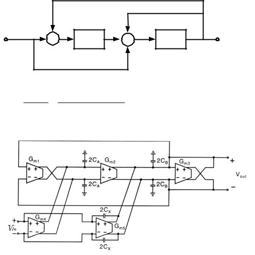
(g) General biquadratic structure
Vo= |
S 2C C V + SC g V + g g V |
||||||||
1 2 |
c |
|
1 m4 |
B |
m2 m5 A |
||||
|
|
||||||||
|
S 2C C |
2 |
+ SC g |
m3 |
+ g |
m2 |
g |
m1 |
|
|
1 |
|
1 |
|
|
||||
* when Vi=VA=VB=VC, the ωo and Q for the poles and zeros can be adjusted by gm's to any desired value.
§15-2.5 Fully Differential Gm-C or OTA-C Filters
1. General first-order filter
H(s)= |
Vout |
= |
K1S + Ko |
|
|
|
|
|
|
|
|
|
|
|||||
|
|
|
S +ω |
|
|
|
|
|
|
|
|
|
|
|
||||
|
V |
|
|
|
o |
|
|
|
|
|
|
|
|
|
||||
|
|
|
in |
|
|
|
|
|
|
|
|
|
|
|
|
|
||
|
|
|
|
|
SCx +Gm1 |
|
|
|
S( |
Cx |
) + |
Gm1 |
|
|
||||
H(s)= |
|
|
|
|
|
|
= |
CA +Cx |
CA +Cx |
|||||||||
|
|
|
|
|
|
|
|
|||||||||||
S(CA +CX ) +Gm2 |
|
S + |
|
Gm2 |
|
|||||||||||||
|
|
|
|
|
|
|
|
|
|
|
|
CA +CX |
|
|
||||
=>Cx=( |
|
|
K1 |
|
)CA , Gm1=Ko(CA+CX), Gm2=ω0(CA+CX) |
|||||||||||||
1 |
|
|
|
|||||||||||||||
|
|
− K1 |
|
|
|
|
|
|
|
|
|
|
|
|||||

15-13 CHUNG-YU WU
§15-3 CMOS Transconductor or OTA
1. CMOS transconductor using triode transistor
*Q9: operated in the triode region.
*Gm can be adjusted by Vgs9 and scaled by the current mirrors Q3/Q7 and Q4/Q8.
*Q5/Q6 are feedback devices to set the drain voltages
of Q1/Q2.
2. CMOS transconductor using varying bias-triode transistors.
* Q3 and Q4 are in the triode region.
* Gm= |
|
|
1 |
|
|
where rds3=rds4= |
|
|
|
|
1 |
|
|
|
|
|
|
|
||
r |
+ r |
+(r |
|| r |
) |
|
2K |
3 |
(V |
|
−V |
) |
|
|
|
|
|||||
|
s1 |
s2 |
ds3 |
ds4 |
|
|
|
|
|
|
|
GS1 |
tn |
|
|
|
|
|
||
|
|
|
|
|
1 |
|
|
|
|
|
1 |
|
|
|
I1 |
|||||
|
|
|
|
|
|
rs1=rs2= |
|
|
|
= |
|
|
|
|
VGS1-Vtn= |
K |
|
|||
|
|
|
|
|
|
g |
m1 |
|
2K |
(V |
−V ) |
1 |
||||||||
|
|
|
|
|
|
|
|
|
|
1 |
|
GS1 |
|
tn |
|
|||||

15-14 CHUNG-YU WU
3. CMOS differential-pair transconductor with floating voltage supply. Conceptual circuit:
Real circuit:
(iD1-iD2)= 4 Keq IB (V1 −V2 )
Gm=4  Keq I B
* 30~50 dB linearity.
4. CMOS bias-offset cross-coupled transconductor.
(i1-i2)=2KVB(V1-V2) Gm=2KVB
*30~50dB linearity


15-16 CHUNG-YU WU
Experimental results on BP filter:
Center frequency 4MHz
TABLE I
EXPERIMENTAL FILTER DATA
Control |
Automatic |
|
Manual |
Passband ripple |
1 dB |
|
0.5 dB |
Stopband attenuation |
|
>60 dB |
|
Bandwidth |
800 KHz |
||
S/N in passband |
≈40dB |
|
75dB |
Distortion (for 0.5Vpp) |
|
0.5% |
|
Max. signal level |
|
1.2 Vpp |
|
Frequency control range |
1 MHz |
|
1.5 MHz |
|
|
|
|
Q-control range |
40% |
|
unlimited |
Offset (reference inverter) |
1mV @ Gain ≈ 50 |
||
|
|
|
|
§15-5 MOSFET-C Filters
*MOSFET-C filters are slower than Gm-C filters
Miller integration.
*Smaller speed
The load of op amps is resistive * Straightforward design methodology

15-17 CHUNG-YU WU
1. Two-transistor integrators.
(a) Active-RC integrator |
|
|
|
(b) Two-transistor MOSFET-C integrator |
|||||
R1 ≡ Rp1 = Rn1 |
R2 ≡ Rp2 = Rn2 |
|
|
|
|
||||
Vdiff ≡Vpo-Vno= |
ino −ipo |
= |
(ip1 +ip2 ) −(in1 +in2 ) |
|
|
|
|||
|
|
|
|
||||||
|
SC |
|
|
SC |
|
|
|
|
|
|
1 |
|
|
|
1 |
|
|
|
|
|
= |
1 |
|
(Vp1 −Vn1 ) + |
1 |
|
(Vp2 −Vn2 ) |
||
|
SR C |
SR |
C |
||||||
|
|
|
|
|
|||||
|
|
|
1 |
1 |
|
2 |
1 |
|
|
2.General biquadratic MOSFET-C filter Active-RC circuit:
MOSFET-C biquadratic filter: