

Therapeutic Micro-Nano Technology BioMEMs - Tejlal Desai & Sangeeta Bhatia
.pdf244 |
|
|
|
SARAH L. TAO AND TEJAL A. DESAI |
||||||
|
|
|
|
|
|
|
|
|
|
|
|
|
|
|
|
|
|
|
|
|
|
|
|
|
|
|
|
|
|
|
|
|
|
|
|
|
|
|
|
|
|
|
|
|
|
|
|
|
|
|
|
|
|
|
A  D
D  G
G
B  E
E  H
H
C  F
F  I
I
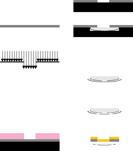
FIGURE 14.3. Process for creating silicon dioxide microdevices. A) Clean silicon wafer. B) Etch stop, sacrificial and device layer deposited respectively on the wafer. C) Positive lithography to define reservoirs in resist. D) Pattern developed. E) Reservoir carved from device layer and remaining photoresist stripped. F) Positive lithography to define microdevice body in resist. G) Pattern developed. H) Device body etched and remaining photoresist stripped. I) Microdevice released from wafer.
straight-walled reservoir. In this case, a reactive ion etch (RIE) with SF6 and O2 was used to carve the reservoirs into the LTO device layer and any remaining photoresist was then removed.
A second positive lithography step was performed to define the microdevice body. Reservoir features on the wafer were aligned to the photomask defining the device body using front side alignment on the mask aligner. After exposure and development of the photoresist, a reactive ion etch with SF6 and O2 was used to etch completely through the unmasked areas of the LTO layer and any remaining photoresist was then removed. The welled microdevices were released into solution by performing a wet etch of the sacrificial polysilicon layer with dilute potassium hydroxide. The potassium hydroxide solution was neutralized and filtered to isolate the microdevices. The microfabrication process for producing silicon dioxide microdevices is shown in Figure 14.3. Figure 14.4 provides examples of the various features which can be implemented in the device utilizing these processes.
14.3.2. Porous Silicon [25]
Porous silicon microdevices were fabricated on a single-side polished silicon <100> p+-type wafer. First, a layer of silicon nitride was deposited by LVCD. The processed
MICRODEVICES FOR ORAL DRUG DELIVERY |
245 |
A |
B |
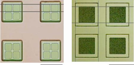
FIGURE 14.4. Silicon dioxide microdevices with different sized reservoirs and bodies. A) 35 μm wells inside a 100 μm body. Bar represents 100 μm. B) 100 μm well inside a 150 μm body. Bar represents 150 μm.
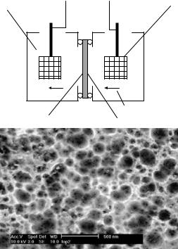
wafers were then spin-coated with a positive resist and photolithography was performed by exposing the frontside of the wafers to ultraviolet light through a photomask defining the area of intended porosity while protecting all other areas of the wafer. The backside of the wafer was then etched with SF6 to strip the layer of silicon nitride. Exposed silicon nitride on the frontside of the wafer was etched with SF6 and the remaining photoresist stripped. The patterned wafers were then anodized and electropolished in a custom built anodization tank with platinum electrodes. An ethanol-hydrofluoric acid (1:1) solution was placed in the cell and a current was applied upon connection of the electrodes to a power supply. Porosification exclusively took place along the anodic side of the silicon wafers. Anodization of the silicon wafer can be described through the following reactions:
Si + 2HF + λh+ → SiF2 + 2H+ + (2 − λ)e− |
(14.1) |
SiF2 + 2HF → SiF4 + H2 |
(14.2) |
SiH4 + 2HF → H2SiF6 |
(14.3) |
Where h+ and e− are the exchanged hole and electron, respectively, and λ is the number of charges exchanged during the elementary step. Pore size and shape depend on the type of silicon used (n/p/p+), the resistivity of the silicon, the current density, and the concentration of hydrofluoric acid solution. A schematic diagram of the double sided Teflon anodization tank in Figure 14.5A and Figure 14.5B shows a scanning electron micrograph of the pores which can be created utilizing this method. The porous particles were separated from the wafer by an electropolishing step in a dilute ethanol-hydrofluoric acid (1:4) solution. The microdevices were then capped by sputtering a thin layer of gold and removed from the wafer utilizing water soluble tape. The entire process for fabricating the porous silicon microdevices is shown in Figure 14.6. A scanning electron micrograph of a porous silicon microdevice is shown in Figure 14.7.
246 SARAH L. TAO AND TEJAL A. DESAI
|
Power Supply |
|
|
HF/Ethanol |
_ |
+ |
Pt Electrode |
Solution |
|
||
|
|
||
|
|
|
|
A |
|
|
Current flow |
Porosification |
Wafer |
B
FIGURE 14.5. A) Schematic of the double-sided Teflon anodization tank. B) Scanning electron micrograph demonstrating pore size distribution between 20–200nm. Courtesy of IMEDD, Inc.
14.3.3. Pol(methyl methacrylate) [24]
PMMA microdevices were fabricated on RCA cleaned silicon <111> p-type wafers. The wafers were first spin-coated with multilayers of PMMA resist film, followed by a layer of positive photoresist. Lithography was used to pattern the device body. After exposure and development of the photoresist, the unmasked area of PMMA was reactive ion etched completely through using an O2 plasma and any remaining resist was subsequently removed.
A second positive lithography step was performed to expose the intended reservoir areas in the PMMA. Device features on the wafer were aligned to the photomask defining the reservoir by front side alignment on the mask aligner. After exposure and development, the exposed PMMA area was then etched with an O2 plasma to carve the reservoirs into the PMMA layer and any remaining photoresist was subsequently removed. The microdevices were then either left on the wafer for further chemical processing or released from the wafer. Since the PMMA adheres to the silicon by linkage to the native oxide layer, the microdevices were released by soaking the wafer in basic solution to break this bonding. The microfabrication process for the PMMA microdevices is depicted in Figure 14.8. A scanning electron micrograph of an array of PMMA microdevices still attached to the silicon wafer is shown in Figure 14.9.
MICRODEVICES FOR ORAL DRUG DELIVERY |
247 |
|||
|
|
|
|
|
|
|
|
|
|
A  F
F
B  G
G
C |
|
H |
|
|
|
|
|
|
|
||
|
|
|
|
||
|
|
|
|
||
|
|
|
|
D |
|
|
|
I |
|
|
|
|
|
|
|
|
|
||
|
|
|
|
|
|
||
|
|
|
|
|
|
||
|
|
|
|
|
|
||
J 


E
FIGURE 14.6. Process for creating porous silicon microdevices. A) Bare silicon wafer. B) Nitride layer is deposited on surface. C) Photolithography used to pattern protective area. D) Resist developed. E) Backside nitride layer stripped. F) Frontside nitride layer patterned and remaining photoresist stripped. G) Pores formed by anodization of exposed silicon. H) Wafer electropolished to separate devices. I) Devices capped by sputtering gold. J) Devices removed from wafer by lifting off with water soluble tape.
14.4. SURFACE CHEMISTRY
Techniques used to associate proteins and polymers include covalent linkage and passive adsorption. Although covalent linkage is often more stable than simple adsorption, it is possible that the stability and function of the conjugates may be impaired. Covalent linkage requires the presence of functional groups on the surface of the substrate. Protein-carrier conjugates have been prepared through activation of hydroxyl, carboxyl, and amino groups
248 |
SARAH L. TAO AND TEJAL A. DESAI |
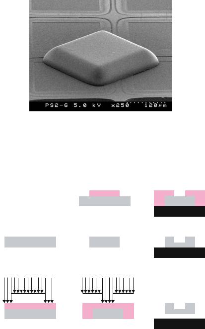
FIGURE 14.7. Scanning electron micrograph of a porous silicon microdevice. Courtesy 8 IMEDD. Inc.
by cyanogenbromide [41], carbodiimide [42], and glutaraldehyde [43, 44], respectively. However, it is uncertain whether these types of crosslinking agents reduce the lectin’s carbohydrate binding abilities. In addition, the amino acid composition, molecular weight, and tertiary structure are so diverse amongst the various types of lectins that direct conjugation to a carrier system would ultimately require a separate modification protocol for
A  D
D  G
G
B  E
E  H
H
C  F
F  I
I
FIGURE 14.8. Process for PMMA microdevices. A) Silicon wafer cleaned by RCA. B) Multilayers of PMMA spun on wafer. C) Photolithography used to pattern body in resist. D) Pattern developed. E) PMMA etched and remaining photoresist stripped. F) Photolithography used to expose reservoir area. G) Pattern developed. H) Reservoir etched from body and remaining photoresist stripped. I) Devices released from wafer.

MICRODEVICES FOR ORAL DRUG DELIVERY |
249 |
FIGURE 14.9. Scanning electron micrograph of a PMMA microdevice array.
each type of lectin. It is instead desirable to have a single method for attaching various lectins to a surface. One such method is to modify the lectin and surface each with one or another of a complementary pair of materials that have a high affinity for each another. A plausible pair of linking materials is avidin and biotin [45]. The bond between avidin and biotin is established very rapidly and is the strongest non-covalent biological interaction between a protein and a ligand. Once the bond is formed it is undisturbed by low pH, exposure to organic solvents and other denaturing agents [45]. By first conjugating avidin to the surface of the carrier, commercially available biotinylated lectins can be attached via avidin-biotin interaction. The basic chemistry for incorporating cytoadhesive properties into this microfabricated platform was performed in three major steps: (1) amine groups were formed on the device; (2) avidin was coupled with convential carbodiimide coupling reagents to form an avidin carboxylate which in turn was reacted with the amine groups of the substrate to form an avidin conjugate; (3) biotinylated lectins were attached to the surface utilizing the strong interaction and affinity between avidin and biotin [23,46] (Figure 14.10).
14.4.1. Aimine Functionalization
Amine groups were formed on the surface of silicon dioxide and porous silicon microdevices through a two-step reaction. First, hydroxyl groups were formed on the silicon surfaces (Figure 14.11A), followed by timed silanization in a (3-aminopropyl)triethoxysilane (APTES) solution to form amine terminated surfaces (Figure 14.11). Heterogeneous modification of PMMA with N-lithioethylenediamine as an aminolyzing agent leads to amination of its ester groups [47, 48]. This reaction renders a layer of amine sites tethered to the PMMA backbone by stable amide groups. First, N-lithioethylenediamine was synthesized by purging reacting ethylenediamine with n-butyllithium under nitrogen atmosphere. Amine groups were placed on the surface of the reservoir side of the microdevices by reacting the wafer bound devices with N-lithioethylenediamine. (Figure 14.12).

250 |
|
|
|
SARAH L. TAO AND TEJAL A. DESAI |
||||
|
|
|
|
NH2 |
NH2 |
|||
A |
|
|
|
B |
|
|
|
|
|
|
|
||||||
|
|
|
|
Amine |
|
|
|
|
|
|
|
|
|
|
|
|
|
|
|
|
|
Functionalization |
|
|
||
|
|
|
|
|
|
|
|
|
Avidin + NHS
+EDC/H2O
|
Avidin |
|
| |
|
C=O |
|
| |
|
N |
O= |
=O |
Lectin |
Lectin |
|
|
| |
| |
C |
|
Biotin |
Biotin |
|
|
Avidin |
Avidin |
Avidin |
Avidin |
| |
| |
| |
| |
C=O |
C=O |
C=O |
C=O |
| |
| |
| |
| |
NH |
NH |
NH |
NH |
Biotin-Lectin
FIGURE 14.10. Surface chemistry used to attach lectins to microdevice surfaces. A) Amine functionalization. B) Avidin immobilization using a hydroxy-succinimide catalyzed carbodiimide reagent. C) Lectin attachment utilizing avidin-biotin attraction and interaction.
A |
+ |
|
|
|
|
|
|
|
|
OH |
||
|
|
|
|
|
|
|
|
|||||
Si |
HCl + H2O2 |
|
Si |
|
|
|||||||
|
|
|
|
|
|
|||||||
B |
|
|
|
OCH2CH3 |
|
|
|
|
OH |
|
||
|
|
|
|
|
|
|
||||||
|
|
|
|
|
|
|
|
|
|
|||
|
|
|
|
|
|
|
|
|||||
|
OH+ CH3CH2O-Si-CH2CH2CH2NH2 |
|
|
|
|
|
|
|||||
Si |
|
|
|
|
|
|
|
|||||
|
|
OH |
|
|
|
|
|
OCH2CH3 |
||||
|
|
|
|
|
|
|
||||||
|
|
|
|
OCH2CH3 |
|
|
|
|||||
|
|
|
|
|
|
|
||||||
|
|
|
|
|
|
Si |
|
|
|
|||
|
|
|
|
|
|
|
|
|
|
|||
|
|
|
|
|
|
|
|
|
|
|
|
|
|
|
|
|
|
|
|
|
O-Si-CH2CH2CH2NH2 |
||||
|
|
|
|
|
|
|
|
|||||
|
|
|
|
|
|
|
|
|
|
|
|
|
|
|
|
|
|
|
|
|
|
|
OCH2CH3 |
||
|
|
|
|
|
|
|
|
|
|
|||
FIGURE 14.11. Surface chemistry for generating amine terminated silicon surfaces. A) Oxidation. B) Silanization.
MICRODEVICES FOR ORAL DRUG DELIVERY |
|
251 |
||||||||||||
|
|
|
CH3 |
|
|
|
|
CH3 |
||||||
|
H2 |
|
|
Li+HN |
NH2 |
H2 |
|
|
||||||
|
|
|
|
|||||||||||
|
( |
C |
|
C |
)x |
+ |
|
( |
C |
|
C |
)x |
||
|
|
|
|
|||||||||||
|
|
|
|
|
|
|
(CH2)2 |
|
|
|
|
|
|
|
|
|
|
|
C = O |
|
|
|
|
|
C = O |
||||
|
|
|
|
|
|
|
|
|
|
|
|
|||
|
|
|
OCH3 |
|
|
|
|
NH |
||||||
|
|
|
|
|
|
|
|
|
|
(H2C)2 |
||||
|
|
|
|
|
|
|
|
|
|
|
|
NH2 |
||
FIGURE 14.12. Chemical reaction for generating aminated PMMA.
14.4.2. Avidin Immobilization
Biological molecules containing carboxyl groups can be reacted with traditional carbodiimide coupling agents to form a reactive intermediate ester that is susceptible to attack by amines. This reaction can be applied to self-assemble a layer of covalently coupled biological molecules to the surface of the silicon dioxide, porous silicon, and PMMA microdevices which have been modified to contain amine sites. Here, molecules of avidin were attached to the microdevice surfaces by timed incubation in a solution of 1-ethyl- 3-(3-dimethylaminopropyl) carbodiimide (EDC), N-Hydroxysuccinimide (NHS), and avidin.
14.4.3. Lectin Conjugation
Lectins were attached to the avidin-modified surfaces by means of an avidin-biotin conjugation method. The avidin-immobilized surfaces were time incubated in a solution of biotinylated lectin optimized for a 1:1 binding ratio of avidin to lectin.
14.5. SURFACE CHARACTERIZATION
Surfaces were characterized after modification utilizing several procedures including chemical assay, fluorescent labeling as well as x-ray photoelectron spectroscopy (XPS) and atomic force microscopy (AFM). A simple, qualitative method using sulfo-succinimidyl- 4-O-(4,4-dimethoxytrityl)-butyrate (s-SDTB) was employed to determine the coverage of amine groups on the substrate surfaces [49]. The reaction of s-SDTB with amine groups on the substrate surface results in stable bonds at alkaline conditions. 4,4 -dimethoxytrityl cation is liberated as a result of this reaction. Since it has a high absorbance at 498 nm and an extinction coefficient of 70,000 M−1 cm−1, concentration can easily be determined by UV/VIS spectrophotometry. As an example, Figure 14.13 shows the concentration of PMMA surface amine groups plotted as a function of reaction time with N-lithioethylenediamine. It was found that a ten minute incubation time rendered approximately 4 nmol cm−2.
252 |
SARAH L. TAO AND TEJAL A. DESAI |
|
6 |
|
|
|
|
|
|
) |
|
|
|
|
|
|
|
2 |
|
|
|
|
|
|
|
cm |
5 |
|
|
|
|
|
|
(nmol |
4 |
|
|
|
|
|
|
Concentration |
3 |
|
|
|
|
|
|
2 |
|
|
|
|
|
|
|
|
|
|
|
|
|
|
|
Surface |
1 |
|
|
|
y=-0.0364x2+0.7375x+0.4497 |
|
|
|
|
|
|
|
R2=1 |
|
|
0 |
|
|
|
|
|
|
|
|
|
|
|
|
|
|
|
|
0 |
2 |
4 |
6 |
8 |
10 |
12 |
Time (min)
FIGURE 14.13. Coverage of immobilized amine groups on the PMMA surface as a function of reaction time.
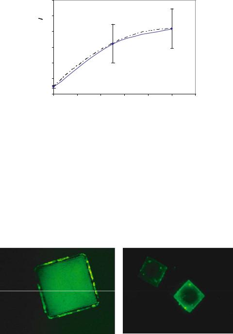
To determine the maximum amount of avidin able to bind successfully to the amineterminated surfaces, the microdevices were conjugated with fluorescein isothyocyanate (FITC) labeled avidin. Figure 14.14 A and B respectively show aminated porous silicon and PMMA microdevices labeled with avidin-FITC.
XPS analysis was performed to ensure the presence of amine groups, avidin, and lectin. Survey scans were taken of substrate samples following amine functionalization, avidin immobilization and lectin conjugation. The changes in elemental surface composition suggest successful modification (Table 14.2). After amine functionalization, an increase of nitrogen was expected. It was shown that this was the case among all three substrates. Analysis of APTES modified surfaces revealed an increase in nitrogen suggesting desirable APTES binding. Furthermore, the amount of carbon also increased after APTES modification. This was expected due to the long hydrocarbon chains of APTES. Analysis of the aminated
FIGURE 14.14. Fluorescently labeled avidin immobilized onto A) aminated porous silicon and B) aminated PMMA.

MICRODEVICES FOR ORAL DRUG DELIVERY |
253 |
TABLE 14.2. Relative elemental surface composition of silicon dioxide, porous silicon and PMMA surfaces.
Sample |
%O |
%N |
%C |
%Si |
|
|
|
|
|
Silicon Dioxide |
31.6 |
1.2 |
26.9 |
40.3 |
Amine-Functionalized Silicon Dioxide |
29.0 |
10.6 |
47.6 |
12.1 |
Avidin-lmmobilized Silicon Dioxide |
24.2 |
11.2 |
50.5 |
12.9 |
Lectin-Conjugated Silicon Dioxide |
20.2 |
15.9 |
59.6 |
0.5 |
Porous Silicon |
59.6 |
0.0 |
8.7 |
31.7 |
Amine-Functionalized Porous Silicon |
42.7 |
2.4 |
35.3 |
19.5 |
Avidin-Immobilized Porous Silicon |
38.9 |
2.5 |
42.4 |
16.3 |
Lectin-Conjugated Porous Silicon |
37.3 |
2.6 |
47.0 |
13.3 |
PMMA |
26.2 |
0.0 |
73.8 |
0.0 |
AmineFunctionalized PMMA |
12.5 |
10.8 |
76.8 |
0.0 |
Avidin-Immoblized PMMA |
19.8 |
12.6 |
67.7 |
0.0 |
Lectin-Conjugated PMMA |
18.7 |
15.1 |
66.2 |
0.0 |
|
|
|
|
|
PMMA surface also showed a significant increase in nitrogen. In addition, the peak area ratio of oxygen to carbon in the amine functionalized PMMA decreased by 12.3% in comparison with that of pristine PMMA. This suggested a successful loss of ester groups and the addition of amide and amine groups on the surface. For silicon substrates, the addition of avidin resulted in an increase in nitrogen composition and a significant increase in carbon. Attachment of lectin resulted in a further increase in nitrogen as well as carbon content on the surface. The indication of protein on the surfaces is supported further by the large increase in the ratio of nitrogen to silicon after protein conjugation. For the PMMA substrate, the addition of avidin and lectin also resulted in a considerable increase of nitrogen on the surface. Successful protein immobilization was confirmed by the increase in the nitrogen to carbon ratio following each procedure.
After chemical modification procedures, subsequent changes in topography were examined using AFM. The surface of pristine, amine-functionalized, avidin-immobilized and lectin-conjugated samples were visualized and characterized by AFM in order to determine the impact of modification on surface coverage. Distinct changes in surface topography were observed on all three substrates. For example, Figure 14.15A shows PMMA surfaces before and after incorporation of amine sites on the surface. Distinct peaks, equally distributed and of relatively uniform height can be seen after amine functionalization. Figure 14.15B shows a comparison of the porous silicon microdevice surfaces before modification and after lectin conjugation. From the AFM images it was determined that the modification procedures did not clog the pores of the microdevice, thereby showing no damage to the releasing mechanism.
14.6. MIOCRODEVICE LOADING AND RELEASE MECHANISMS
Like the microfabrication processes used to create the welled and porous devices, the mechanisms used to load the devices remain very different. These approaches are described below.