Книги+1 / 2013 [Chandan_Kumar_Sarkar]_Technology_CAD
.pdf344 |
Technology Computer Aided Design: Simulation for VLSI MOSFET |
design methodology is required. Statistical design methodology has become indispensable for the present VLSI circuits. Precise characterization of process variability is essential for variability-aware statistical circuit design.
7.9.1 Classification of Process Variability
From a circuit design perspective, the process variations are classified into two types: intra-die and inter-die variations. The intra-die variations are defined as the parametric changes of identical MOS transistors across a short distance, while the inter-die variations refer to such changes for identical MOS transistors separated by longer distance or fabricated at different times [24]. Thus intra-die variations are deviations occurring within a die. On the other hand, the inter-die variations are deviations occurring from die-to-die, wafer-to-wafer, and lot-to-lot. The wafer-to-wafer variations are caused usually by some change in machine conditions along time of manufacturing apparatus. The die-level variations typically originate from lithography steps, because pattern exposure is performed die-to-die. Imperfections in reticles or non-uniformity in the lens system sometimes causes die-level variations. The intra-die variations are significant in sub-90 nm technology and are of critical concern to the IC designers. The intra-die variations have two components: systematic and random. The systematic variations include the variations caused due to optical proximity corrections, phase-sifting mask and layoutinduced strain, and well proximity effect [24]. On the other hand, the random variations include variations due to random discrete dopant (RDD), line edge roughness (LER), line width roughness (LWR), oxide thickness variation (OTV), poly-silicon gate/metal gate granularity, and interface roughness. In this chapter, we restricted ourselves to the local component of intra-die process variations, which is of serious concern in the nanoscale regime.
7.9.2 Sources of Random Intra-Die Process Variations and Their Effects
In this subsection, the major sources of process variations are identified and their effects on the device performances are discussed.
7.9.2.1 Random Discrete Dopant (RDD)
With the scaling of the transistor in sub-90 nm technology, it has been found that the number of dopant atoms within the channel of a transistor becomes discrete and is a statistical quantity. In 1 μm technology, the number of dopant atoms in the channel is near about 5000, whereas that in a 32-nm technology node is less than 100. The random fluctuations of the number and position of the dopant atoms in the channel of a MOS transistor cause device-to-device variations of electrical performances which is referred to as the random discrete dopant effect [25].
RDD is considered to be the major contributor to performance mismatch of identical MOS transistors placed very close to each other. Considering
346 |
Technology Computer Aided Design: Simulation for VLSI MOSFET |
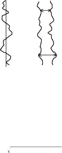
Definition of LER |
Definition of LWR |
FIGURE 7.39
Microscopic view of channel length along width illustrating LER and LWR.
7.9.2.3 Oxide Thickness Variation (OTV)
Another important source of random intra-die process variability is atomicscale oxide thickness variation. With the downscaling of the physical gate oxide thickness up to 1 nm, it becomes equivalent to approximately five interatom spacing. Through experimentation, it has been observed that the oxide thickness roughly varies by one or two atomic spacing [30]. The oxide thickness variation occurs primarily due to interface roughness. The oxide thickness variations also lead to variations of all performances related to oxide thickness either implicitly or explicitly. The threshold voltage variations due to oxide thickness are also statistically independent of RDD and LER, so that (7.167) is transformed to
σVT ,total = (σVT ,RDD )2 + (σVT ,LER )2 + (σVT ,OTV )2 |
(7.168) |
7.9.3 Characterization of Process Variability
Accurate characterization of process variability is a challenging task. The present subsection highlights the conventional approach and briefly discusses the new approaches. The development of an accurate characterization procedure is an important research topic.
7.9.3.1 Design Corner Approach
From an IC designer’s point of view, the collective effects of process variations are lumped into their effects on the performances of a circuit. These define the
MOSFET Characterization for VLSI Circuit Simulation |
347 |
Fast |
|
FF |
|
|
|
|
SF |
|
PMOS |
TT |
|
|
|
|
|
|
FS |
|
SS |
|
Slow |
|
|
Slow |
NMOS |
Fast |
|
|
FIGURE 7.40
Design corners.
design or process corners. The term corner refers to an imaginary box that surrounds the guaranteed performance of the circuits, as shown in Figure 7.40. The corners for analog applications are slow NMOS and slow PMOS (SS) to characterize the worst-case speed and fast NMOS and fast PMOS (FF) to characterize the worst-case power. The corners for digital applications are fast NMOS and slow PMOS (FS) to characterize the worst-case logic 1 and slow NMOS and fast PMOS (SF) to characterize the worst-case logic 0. The typical (TT) case characterizes the nominal design of the transistors. The corner parameters are generated by deviating the selected process-sensitive SPICE model parameters by a fixed number n of standard deviation σ. For example, an arbitrary SPICE parameter si of the typical model file is represented through
si = si0 ± nσ |
(7.169) |
In (7.169), n is selected to set the fixed lower and upper limits of the worstcase models. The direction of the deviation from the mean/typical value si0 depends on whether increasing or decreasing the parameter makes the performance worse. This is usually determined by the sensitivity analysis, by computing the derivative of the performance with respect to the chosen SPICE parameter, and by considering the sign of the derivative.
The advantage of this design corner approach is that the corner models are supplied to the designers so that the circuit can be simulated at each of the process corners for statistical characterization of the effects of process variabilities on circuit performances. However, this approach has two serious limitations. First, it has the significant risk of overor underestimation of the process variations and their impact on the design. Overestimation makes the task of designing the circuits difficult such that the performances meet
348 |
Technology Computer Aided Design: Simulation for VLSI MOSFET |
the specifications at all the corners. On the other hand, underestimation may lead to manufacturability problems and eventual loss in yield. The second problem is that while generating the corner parameters, the correlations between the device parameters are ignored. This approach therefore does not provide adequate information about the robustness of the design.
7.9.3.2 Monte Carlo Simulation Approach
The Monte Carlo simulation technique is a stochastic technique widely used for statistical characterization of the performance parameter variations due to process variability. The Monte Carlo approach allows direct estimation of the yield of a VLSI circuit. In this technique, the crucial SPICE parameters are sampled from a pre-defined statistical distribution conforming to the process specification. This forms a large database of process-related SPICE parameters, and for each sample of the database, the performance parameters of the circuit are simulated through SPICE simulation. The statistical distributions of the performance parameters corresponding to each sample of the process database are estimated by determining the mean and the standard deviation. The method is very general and accurate for statistical characterization. The problem with the Monte Carlo-based approach is that hundreds of simulation runs have to be performed and depending upon the complexity of the circuit, the entire procedure may take several hours. However, some strategies are available to reduce the sample size, such as variance reduction techniques, stratified sampling, etc.
7.9.3.3 Statistical Corner Approach
The basic idea of the statistical corner model approach is to make the design corner approach more realistic by adding a realistic value of the standard deviation of the corresponding model parameter to its nominal value following (7.158). The value of each σ is obtained from the distribution of a large set of production data. The production data are actual measurement data collected over multiple dies, wafers, and lots. In the absence of actual measurement data, which are fairly common for new process technology, the production data may consist of calibrated TCAD simulation results. The electrical test data, whatever the collection procedure, are mapped to the appropriate SPICE parameters either directly or through some extraction procedure [31]. A statistical corner-based approach is thus more realistic compared to the conventional design corner approach discussed earlier and is faster compared to the Monte Carlo approach.
7.9.4 Simulation Results and Discussion
This section presents SPICE simulation results for statistical characterization of three important performance parameters of an n-channel MOS transistor.
MOSFET Characterization for VLSI Circuit Simulation |
349 |
These are (1) threshold voltage VT , (2) OFF current IOFF , and (3) subthreshold slope S. The intra-die variations studied are random discrete dopants, line edge roughness, and oxide thickness variations. The Monte Carlo simulation technique has been utilized using 45-nm PTM model file.
7.9.4.1 Statistical Characterization of RDD
The effects of RDD on device performances are studied through SPICE simulation by varying the threshold voltage SPICE parameter VTHO. The reason behind such a selection is that with the variation of dopant number and hence the doping concentration within the channel, the long channel threshold voltage is primarily affected. In order to characterize the amount of variation of this parameter, there are two approaches. The first is to extract from TCAD simulation results, and the second is to calculate it from (7.164). Because the present work attempts to provide only the philosophy of the characterization procedure, the latter approach is performed, although the first one is preferred for accurate characterization.
The effective channel length and width of the chosen MOS transistor are 37.5 nm and 120 nm, respectively. The substrate doping concentration is 3.24E10/cm3, and the electrical oxide thickness is 1.75 nm. Substituting the necessary values, σVT ,RDD is calculated from (7.158) and is found to be 17.71 mV. The same amount of variation is taken for the SPICE parameter VTHO. For Monte Carlo simulation, a set of 1000 samples has been chosen. The distribution of the SPICE parameter VTHO is considered to be Gaussian. The simulation is performed both at low drain bias and high drain bias—that is,
VDS = 50mV and VDS = 1V.
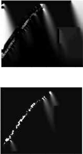
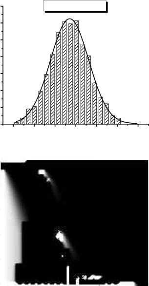
The variations of the gate characteristics of the transistor due to RDD at low and high drain bias are shown in Figures 7.41(a) and 7.41(b), respectively. The performance samples are characterized by four measures: mean, standard deviation, skew factor, and kurtosis. These are summarized in Tables 7.4 and 7.5 for low drain bias and high drain bias, respectively. The distributions of the samples for the high drain bias case are shown in Figures 7.42(a) through 7.42(c). The distribution of threshold voltage is Gaussian, whereas that for IOFF and S are log-normal.
7.9.4.2 Statistical Characterization of Line Edge Roughness (LER)
Line edge roughness is the distortion of the gate edge. In order to characterize the distortion of the gate edge, a simplified model of a rough line as shown in Figure 7.43 is considered. The roughness in the gate edge is characterized by high-frequency roughness and low-frequency roughness. The gate is divided into segments with characteristic width WC, which characterizes the change at which the low frequency part changes the gate length. Within this portion, only high-frequency roughness is present. Assuming