

Broadband Packet Switching Technologies
.pdf96 SHARED-MEMORY SWITCHES
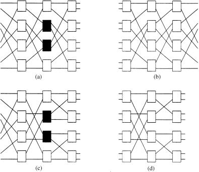
to input i of the jth switch element in the fifth stage. Repeating in this way, a network of arbitrary large size can be theoretically obtained. For N s 8k, the Benes network constructed using 8-port switch elements has 2 k y 1 stages. Since k s log8 N, the number of switch elements scales in proportion to N log8 N, which is the best possible scaling characteristic. In w16x, it is shown that when dynamic load distribution is performed in the first k y 1 stages of the Benes network, the load on the internal data paths of the switching network cannot exceed the load on the external ports; that is, the network achieves ideal load balancing. This is true for both point-to-point and multipoint traffic.
4.4.2 Concentrator-Based Growable Switch Architecture
A concentrator-based growable switch architecture is shown in Figure 4.12 w4x. The 8 8 output ATM switches Žwith the shared-memory structure. are each preceded by an N 8 concentrator. The N 8 concentrator is preceded by a front-end broadcast network Ži.e., a memoryless cell distribution network.. The concentrators are preceded by address filters that only accept cells that are destined to its group of dedicated outputs. The valid cells in each concentrator are then buffered for a FIFO operation. In other words, each concentrator is an N-input 8-output FIFO buffer. The actual ATM cell switching is performed in the ATM output switch. Obviously, this is increasingly challenging as N becomes large. For instance, a 512 8 concentrator can be built using a column of eight 64 8 concentrators followed by another 64 8 concentrator. At 2.5 Gbitrs per port, a 64 64 switch has a capacity of 160 Gbitrs, and a 512 512 switch has a capacity of 1.28 Tbitrs.
Fig. 4.12 A concentrator-based growable switch architecture.
MULTICAST SHARED-MEMORY SWITCHES |
97 |
4.5 MULTICAST SHARED-MEMORY SWITCHES
Of the various ATM switch architectures, the shared-memory switch provides the greatest benefits. Since its memory space is shared among its switch ports, it achieves high buffer utilization efficiency. Under conditions of identical memory size, the cell-loss probability of the shared-memory switches is smaller than that of output-buffered switches. Additionally, multicast operations can be easily supported by this switch architecture. In this section, some classes of multicast shared-memory switches are described along with their advantages and disadvantages.
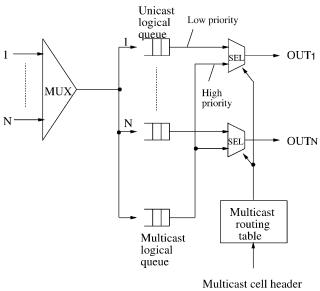
4.5.1 Shared-Memory Switch with a Multicast Logical Queue
The simplest way to implement multicasting in a shared-memory switch is to link all multicasting cells in a logical queue as shown in Figure 4.13. The advantage of this approach is that the number of logical queues that need to be updated in every cell slot is minimized. The multicast routing table stores routing information, such as a bit map of output ports to which the multicast cells are routed. In this example, multicast cells always have higher priority than unicast cells. That is called strict priority, where unicast cells will be served only when the multicast logical queue is empty or the multicast HOL cell is not destined for the output port for which they are destined. Of course, there can be other service policies between unicast and multicast cells
Fig. 4.13 A shared-memory ATM switch with a multicast logical queue.
98 SHARED-MEMORY SWITCHES
than the strict priority. For instance, they can be served in a round-robin manner, or a weighted round-robin manner with the weight depending on, for example, the ratio of unicast and multicast traffic load. However, the major disadvantage of this approach is there may be HOL blocking for the multicast logical queue when schemes other than the strict priority are used. This is because when the multicast HOL cell is blocked because of yielding its turn to unicast cells, it may block other multicast cells that are behind it, though they could otherwise have been transmitted to some idle outputs.
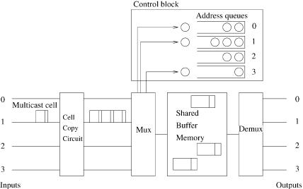
4.5.2 Shared-Memory Switch with Cell Copy
In this approach, a multicast cell is replicated into multiple copies for all its multicast connections by a cell-copy circuit located before the routing switch. Bianchini and Kim w7x proposed a nonblocking cell-copy circuit for multicast purpose in an ATM switch. Each copy is stored in the SBM. The address for each copy is queued in output address queues ŽAQs..
Figure 4.14 shows an example of a shared-memory switch with a cell-copy circuit. A multicast cell arrives and is replicated into three copies for output ports 0, 1, and 3. These three copies of the cell are stored at different locations of the shared buffer memory. Meanwhile, their addresses are stored in corresponding AQs. In this scheme, after replicating the multicast cell, each copy is treated the same way as an unicast cell. It provides fairness among ATM cells. The major disadvantage of this approach is that, in the worst case, N cells might be replicated to N 2 cells. Thus, the number of replicated cells to the SBM in each switch cycle could be OŽ N 2 .. Since only
Fig. 4.14 A shared-memory ATM switch with cell-copy circuit.
MULTICAST SHARED-MEMORY SWITCHES |
99 |
at most N cells could be transmitted, this would result in storing OŽ N 2 . cells in each cycle. For a finite memory space, it would result in considerable cell loss. The replication of multicast cells would also require OŽ N 2 . cells to be written to the SBM, which would further limit the switch size on account of the memory speed. Moreover, adding the cell-copy circuit in the switch increases the hardware complexity.
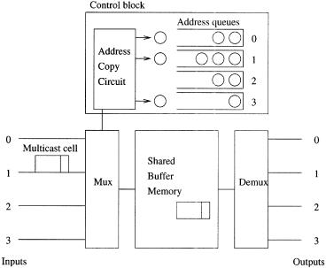
4.5.3 Shared-Memory Switch with Address Copy
Saito et al. proposed a new scheme that requires less memory for the same cell loss probability w13x. A similar architecture was proposed in w11x. In this scheme, an address-copy circuit is used in the controller. When a multicast cell arrives, only a single copy is stored in the SBM. Its address is copied by the address-copy circuit and queued into multiple address queues, as shown in Figure 4.15. The multicast cell will be read multiple times to different output ports. Thereafter, the cell’s address becomes available for the next arriving cells.
In this architecture, multicast cell counters ŽMCCs. are required to hold the number of copies of each multicast cell. The MCC values are loaded as new cells Žunicast or multicast. arrive and are decreased by one each time a copy of a cell is read out from the SBM.
Fig. 4.15 A shared-memory ATM switch with address-copy circuit.
100 SHARED-MEMORY SWITCHES
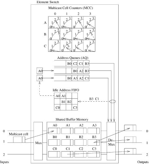
Fig. 4.16 An example of multicast function in an address-copy switch.
Figure 4.16 illustrates an example of a 3 3 ATM switch. In this example, a multicast cell arriving at input port 1 is destined for output ports 1 and 2. The multicast cell is written into A0 in the SBM, and its address is provided by an IAF. Other vacant cells’ addresses stored in the IAF are A1, B1, B2, C0, and C3. A0 is copied and queued in the Address queues 1 and 2. At the same time, the MCC of A0 is set to two. Another multicast cell stored at B3 is destined for output ports 0 and 1. As it is transmitted to both output ports 0 and 1, the associated MCC becomes zero and the address B3 is released to
REFERENCES 101
the IAF. Within the same time slot, the cell stored at C1 is read to output port 2. Since it still has one copy to be sent to output port 0, its address C1 is not released until it is transmitted to output port 0.
Although in each time slot the maximum number of cells to be written into the buffer is N, the number of replications of cell addresses for incoming cells could be OŽ N 2 . in the broadcast case, which still limits the switch size. More specifically, since the address queues or the MCCs are in practice stored in the same memory, there can be up to N 2 memory accesses in each cell slot, which may cause a system bottleneck for a large N.
REFERENCES
1.H. Ahmadi and W. E. Denzel, ‘‘A survey of modern high-performance switching techniques,’’ IEEE J. Select. Areas Commun., vol. 7, no. 7, pp. 1091 1103, Sep. 1989.
2.T. R. Banniza, G. J. Eilenberger, B. Pauwels, and Y. Therasse, ‘‘Design and technology aspects of VLSI’s for ATM switches,’’ IEEE J. Select. Areas Commun., vol. 9, no. 8, pp. 1255 1264, Oct. 1991.
3.N. Endo, T. Kozaki, T. Ohuchi, H. Kuwahara, and S. Gohara, ‘‘Shared buffer memory switch for an ATM exchange,’’ IEEE Trans. Commun., vol. 41, no. 1,
pp.237 245, Jan. 1993.
4.K. Y. Eng and M. J. Karol, ‘‘State of the art in gigabit ATM switching,’’Proc. IEEE BSS ’95, Poland, pp. 3 20, Apr. 1995.
5.W. Fischer, O. Fundneider, E. H. Goeldner, and K. A. Lutz, ‘‘A scalable ATM switching system architecture,’’ IEEE J. Select. Areas Commun., vol. 9, no. 8,
pp.1299 1307, Oct. 1991.
6.J. Garcia-Haro and A. Jajszczyk, ‘‘ATM shared-memory switching architectures,’’ IEEE Network Magazine, pp. 18 26, Jul.rAug. 1994.
7.R. P. Bianchini Jr. and H. S. Kim, ‘‘Design of a nonblocking shared-memory copy network for ATM,’’ Proc. IEEE INFOCOM ’92, pp. 876 885, 1992.
8.H. S. Kim, ‘‘Design and performance of multinet switch: a multistage ATM switch architecture with partially shared buffers,’’ IEEErACM Trans. Networking, vol. 2, no. 6, pp. 571 580, Dec. 1994.
9.T. Kozaki, N. Endo, Y. Sakurai, O. Matsubara, M. Mizukami, and K. Asano, ‘‘32 32 shared buffer type ATM switch VLSI’s for B-ISDN’s,’’ IEEE J. Select. Areas Commun., vol. 9, no. 8, pp. 1239 1247, Oct. 1991.
10.H. Lee, K. H. Kook, C. S. Rim, K. P. Jun, and S. K. Lim, ‘‘A limited shared output buffer switch for ATM,’’ Fourth Int. Conf. on Data Commun. Systems and Their Performance, Barcelona, pp. 163 179, Jun. 1990.
11.T.-H. Lee and S. J. Liu, ‘‘Multicasting in a shared buffer memory switch,’’ Proc. IEEE TENCON ’93, Beijing, pp. 209 212, 1993.
102 SHARED-MEMORY SWITCHES
12.K. Oshima, H. Yamanaka, H. Saito, H. Yamada, S. Kohama, H. Kondoh, and Y. Matsuda, ‘‘A new ATM switch architecture based on STS-type shared buffering and its LSI implementation,’’ Proc. IEICE, pp. 359 363, 1992.
13.H. Saito, H. Yamanaka, H. Yamada, M. Tuzuki, H. Kondoh, Y. Matsuda, and K. Oshima, ‘‘Multicast function and its LSI implementation in a shared multibuffer ATM switch,’’ Proc. IEEE Infocom ’94, pp. 315 322, 1994.
14.K. J. Schultz and P. G. Gulak, ‘‘CAM-based single-chip shared buffer ATM switch,’’ Proc. IEEE ICC ’94, pp. 1190 1195, May 1994.
15.F. A. Tobagi, ‘‘Fast packet switch architectures for broadband integrated services digital networks,’’ Proc. IEEE, vol. 78, no. 1, pp. 133 167, Jan. 1990.
16.T. Cheney, J. A. Fingerhut, M. Flucke, and J. S. Turner, ‘‘Design of a Gigabit ATM Switch,’’ Proc. IEEE INFOCOM ’97, pp. 1392 1399, 1997.
Broadband Packet Switching Technologies: A Practical Guide to ATM Switches and IP Routers
H. Jonathan Chao, Cheuk H. Lam, Eiji Oki
Copyright 2001 John Wiley & Sons, Inc. ISBNs: 0-471-00454-5 ŽHardback.; 0-471-22440-5 ŽElectronic.
CHAPTER 5
BANYAN-BASED SWITCHES
The very early theoretical work on multistage interconnection networks ŽMINs. was done in the context of circuit-switched telephone networks w7, 4x. The aim was to design a nonblocking multistage switch with number of crosspoints less than in a single-stage crossbar switch. After many such networks were studied and introduced for interconnecting multiple processors and memories in parallel computer systems, several types of them, such as banyan and shuffle-exchange networks, were proposed w20, 12, 21x as switching fabrics because in them several cells can be routed in parallel and the switching function can be implemented regularly in hardware.
In this chapter, we describe banyan-family switches, which have attracted many researchers, over more than two decades, for building interconnection networks. Section 5.1 classifies banyan-family switch architectures according to their nature and properties. Section 5.2 describes Batcher-sorting network switch architecture. Section 5.3 introduces output-contention resolution algorithms in banyan-family switches. Section 5.4 describes the Sunshine switch, which extends the Batcher banyan switching architecture. Section 5.5 describes some work on deflection routing over banyan-family networks. Section 5.6 introduces a self-routing copy network where the nonblocking property of banyan networks is generalized to support multicasting.
5.1 BANYAN NETWORKS
The banyan class of interconnection networks was originally defined in w9x. It has the property that there is exactly one path from any input to any output.
103
104 BANYAN-BASED SWITCHES
Fig. 5.1 Four different banyan-class networks: Ža. shuffle-exchange Žomega. network; Žb. reverse shuffle-exchange network; Žc. narrow-sense banyan network; Žd. baseline network. We can see that Ža. and Žb. are isomorphic by interchanging the two shaded nodes.
Figure 5.1 shows four networks belonging to this class: the shuffle-exchange network Žnarrow-sense also called the omega network., the reverse shuffleexchange network, the narrow-sense banyan network, and the baseline network.
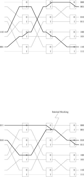
The principal common properties of these networks are: Ž1. they consist of n s log2 N stages and Nr2 nodes per stage,1 Ž2. they have the self-routing property that the unique n-bit destination address can be used to route a cell from any input to any output, each bit for one stage, and Ž3. their regularity and interconnection pattern are very attractive for VLSI implementation. Figure 5.2 shows a routing example in an 8 8 banyan network, where the bold lines indicate the routing paths. On the right hand side, the address of each output destination is labeled as a string of n bits, b1 bn. A cell’s destination address is encoded into the header of the cell. In the first stage, the most significant bit b1 is examined. If it is a 0, the cell will be forwarded to the upper outgoing link; if it is a 1, the cell will be forwarded to the lower outgoing link. In the next stage, the next most significant bit b2 will be
1A regular N N network can also be constructed from identical b b switching nodes in k stages, where N s bk.
BANYAN NETWORKS |
105 |
Fig. 5.2 An 8 8 banyan network.
examined and the routing performed in the same manner.
The internal blocking refers to the case where a cell is lost due to the contention on a link inside the network. Figure 5.3 shows an example of internal blocking in an 8 8 banyan network. However, the banyan network will be internally nonblocking if both conditions below are satisfied:
there is no idle input between any two active inputs;
the output addresses of the cells are in either ascending order or descending order.
Fig. 5.3 Internal blocking in an 8 8 banyan network.