

Broadband Packet Switching Technologies
.pdfPERFORMANCE 207
more, the number of blocked links can be dynamically changed based on the output buffer’s congestion situation.
Here, we only consider the QL scheme Žcell loss at both input and output buffers.. In the abacus switch, cell loss can occur at input and output buffers, but not in the MGN. Figure 7.12 shows input buffer overflow probabilities with different average burst lengths . For uniform random traffic, an input buffer with a capacity of a few cells is sufficient to maintain the buffer overflow probability less than 10y6 . As the average burst length increases, so does the cell loss probability. For an average burst length of 15, the required input buffer size can be a few tens of cells for the buffer overflow probability of 10y6 . By extrapolating the simulation result, the input buffer size is found to be about 100 cells for 10y10 cell loss rate.
Figure 7.13 shows output buffer overflow probabilities with different average burst lengths. Here, Bo is the normalized buffer size for each output. It is shown that the required output buffer size is much larger than the input buffer size for the same cell loss probability.
Fig. 7.13 Output buffer overflow probability vs. output buffer size Žsimulation..
208 THE ABACUS SWITCH
Fig. 7.14 Block diagram of the ARC chip.
7.5 ATM ROUTING AND CONCENTRATION CHIP
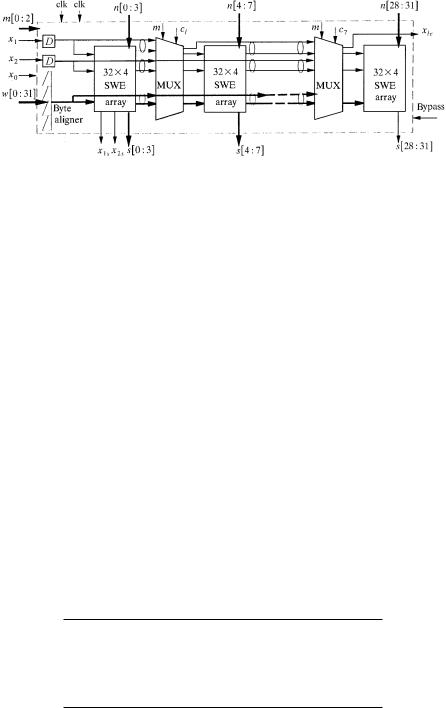
An application-specific integrated circuit ŽASIC. has been implemented based on the abacus switch architecture. Figure 7.14 shows the ARC chip’s block diagram. Each block’s function and design are explained briefly in the
following |
sections. Details |
can be found in w3x. The ARC chip contains |
32 32 |
SWEs, which are |
partitioned into eight SWE arrays, each with |
32 4 SWEs. A set of input data signals, ww0 : 31x, comes from the IPCs. Another set of input data signals, nw0 : 31x, either comes from the output, sw0 : 31x, of the chips on the above row, or is tied to high for the chips on the first row Žin the multicast case.. A set of the output signals, sw0 : 31x, either go to the north input of the chips one row below or go to the output buffer.
A signal x0 is broadcast to all SWEs to initialize each SWE to across state, where the west input passes to the east and the north input passes to the south. A signal x1 specifies the address bitŽs. used for routing cells, while x2 specifies the priority field. Other output signals x propagate along with cells to the adjacent chips on the east or south side.
Signals mw0 : 1x are used to configure the chip into four different group sizes as shown in Table 7.1: Ž1. eight groups, each with 4 output links, Ž2. four groups, each with 8 output links, Ž3. two groups, each with 16 output links, and Ž4. one group with 32 output links. A signal mw2x is used to configure the
TABLE 7.1 Truth Table for Different Operation Modesa
mw1x |
mw0x |
Operation |
|
|
|
0 |
0 |
8 groups with 4 links per group |
0 |
1 |
4 groups with 8 links per group |
1 |
0 |
2 groups with 16 links per group |
1 |
1 |
1 group with 32 links per group |
a mw2x s 1 multicast, mw2x s 0 unicast.
ATM ROUTING AND CONCENTRATION CHIP |
209 |
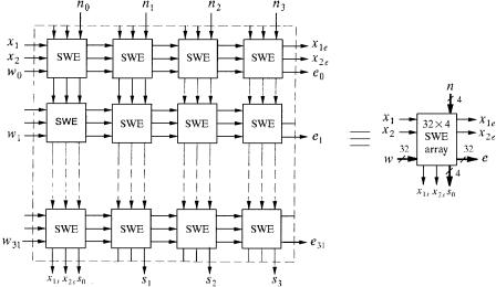
Fig. 7.15 32 4 SWE array.
chip to either unicast or multicast application. For the unicast case, mw2x is set to 0, while for the multicast case, mw2x is set to 1.
As shown in Figure 7.15, the SWEs are arranged in a crossbar structure, where signals only communicate between adjacent SWEs, easing the synchronization problem. ATM cells are propagated in the SWE array similarly to a wave propagating diagonally toward the bottom right corner. The signals x1 and x2 are applied from the top left of the SWE array, and each SWE distributes them to its east and south neighbors. This requires the same phase of the signal arriving at each SWE. x1 and x2 are passed to the neighbor SWEs Žeast and south. after one clock cycle delay, as are the data signals Žw and n.. A signal x0 is broadcast to all SWEs Žnot shown in Figure 7.15. to precharge an internal node in the SWE in every cell cycle. The output signal x1 e is used to identify the address bit position of the cells in the first SWE array of the next adjacent chip.
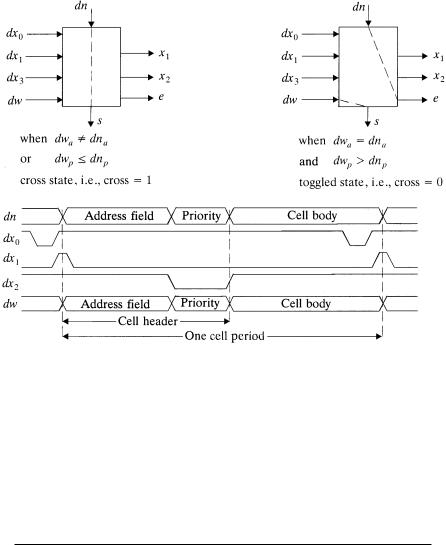
The timing diagram of the SWE input signal and its two possible states are shown in Fig. 7.16. Two bit-aligned cells, one from the west and one from the north, are applied to the SWE along with the signals dx1 and dx2 , which determine the address and priority fields of the input cells. The SWE has two states: cross and toggle. Initially, the SWE is initialized to a cross state by the signal dx0 , i.e., cells from the north side are routed to the south side, and cells from the west side are routed to the east side. When the address of the cell from the west Ždwa. is matched with the address of the cell from the north Ždna., and when the west’s priority level Ždwp . is higher than the north’s Ždnp ., the SWEs is toggled. The cell from the west side is then routed
210 THE ABACUS SWITCH
Fig. 7.16 Two states of the switch element.
to the south side, and the cell from the north is routed to the east. Otherwise, the SWE remains at the cross state.
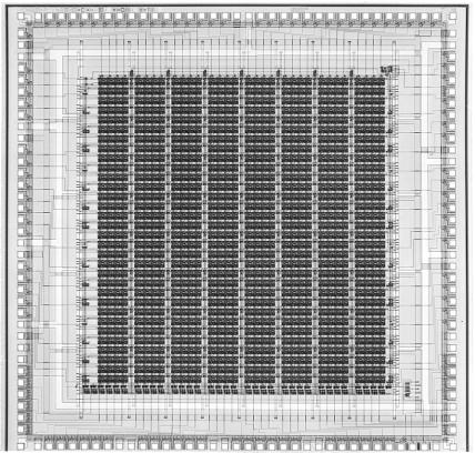
The 32 32 ARC chip has been designed and fabricated using 0.8- m CMOS technology with a die size of 6.6 mm 6.6 mm. Note that this chip is pad-limited. The chip has been tested successfully up to 240 MHz, and its characteristics are summarized in Table 7.2. Its photograph is shown in Figure 7.17.
TABLE 7.2 Chip Summary
Process technology |
0.8- m CMOS, triple metal |
Number of switching elements |
32 32 |
Configurable group size |
4, 8, 16, or 32 output links |
Pin count |
145 |
Package |
Ceramic PGA |
Number of transistors |
81,000 |
Die size |
6.6 6.6 mm2 |
Clock signals |
Pseudo ECL |
Interface signals |
TTLrCMOS inputs, CMOS outputs |
Maximum clock speed |
240 MHz |
Worst case power dissipation |
2.8 W at 240 MHz |
|
|
ENHANCED ABACUS SWITCH |
211 |
Fig. 7.17 Photograph of the ARC chip. Ž 1997 IEEE..
7.6 ENHANCED ABACUS SWITCH
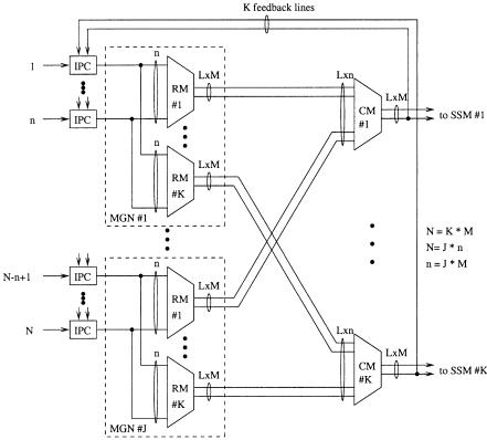
This section discusses three approaches of implementing the MGN in Figure 7.1 to scale up the abacus switch to a large size. As described in Section 7.2, the time for routing cells through an RM and feeding back the lowest-priority information from the RM to all IPCs must be less than one cell slot time. The feedback information is used to determine whether or not the cell has been successfully routed to the destined output groupŽs.. If not, the cell will continue retrying until it has reached all the desired output groups. Since each SWE in an RM introduces a 1-bit delay as the signal passes it in either direction, the number of SWEs between the uppermost link and the rightmost link of an RM should be less than the number of bits in a cell. In other words, N q LM y 1 424 Žsee Section 7.2.. For example, if we choose M s 16, L s 1.25, the equation becomes N q 1.25 16 y 1 424. The maximum value of N is 405, which is not large enough for a large-capacity switch.
212 THE ABACUS SWITCH
7.6.1 Memoryless Multistage Concentration Network
One way to scale up the abacus switch is to reduce the time spent on traversing cells from the uppermost link to the rightmost link in an RM Žsee Fig. 7.2.. Let us call this time the routing delay. In a single-stage abacus switch, the routing delay is N q LM y 1, which limits the switch size, because it grows with N.
To reduce the routing delay, the number of SWEs that a cell traverses in an RM must be minimized. If we divide an MGN into many small MGNs, the routing delay can be reduced. Figure 7.18 shows a two-stage memoryless multistage concentration network ŽMMCN. architecture that can implement a large-capacity abacus switch. It consists of N IPCs, J Žs nrM . MGNs, and K Žs NrM . concentration modules ŽCMs.. Each MGN has K RMs, and
each RM has n input links and |
LM output links. Each CM has J LM |
input links and LM output links. |
|
Fig. 7.18 A two-stage memoryless multistage concentration network.
ENHANCED ABACUS SWITCH |
213 |
After cells are routed through the RMs, they need to be further concentrated at the CMs. Since cells that are routed to the CM always have correct output group addresses, we do not need to perform a routing function in the CM. In the CM, only the concentration function is performed by using the priority field in the routing information. The structure and implementation of the RM and the CM are identical, but the functions performed are slightly different.
Recall that each group of M output ports requires LM routing links to achieve high delay throughput performance. The output expansion ratio of the RM must be equal to or greater than that of the CM. If not, the multicast contention resolution algorithm does not work properly. For example, let us assume that N s 1024, M s 16, and n s 128. Consider the case that there are 16 links between an RM and a CM, while there are 20 links between a CM and an SSM. If all 128 cells of MGN 1 are destined for output group 1 and no cells from other MGNs are destined for output group 1, the feedback priority of CM 1 will be the priority of the address broadcaster, which has the lowest priority level. Then, all 128 cells destined for output group 1 are cleared from the IPCs of MGN 1, even though only 20 cells can be accepted in the SSM. The other 108 cells will be lost. Therefore, the output expansion ratio of the RM must be equal to or greater than that of the CM.
Let us define n as the module size. The number of input links of an RM is n, and the number of input links of the CM is J LM. By letting n s JM, the number of input links of the CM is of the same order as the number of input links of the RM, because we can engineer M so that L is close to one.
In the MMCN, the feedback priorities ŽFPs. are extracted from the CMs and broadcast to all IPCs. To maintain the cell sequence integrity from the same connection, the cell behind the HOL cell at each IPC cannot be sent to the switch fabric until the HOL cell has been successfully transmitted to the desired output portŽs.. In other words, the routing delay must be less than one cell slot. This requirement limits the MMCN to a certain size.
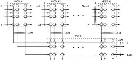
Cells that have arrived at a CM much carry the address of the associated output group Žeither valid cells or dummy cells from the RM’s AB.. As a result, there is no need of using the AB in the CM to generate dummy cells to carry the address of the output group. Rather, the inputs that are reserved for the AB are replaced by the routing links of MGN1. Thus, the routing delay of the two-stage MMCN is n q Ž J y 1.Ž LM . q LM y 1, as shown in Figure 7.19, which should be less than 424. Therefore, we have the following
equation by replacing J with nrM: n q ŽnrM y 1.Ž LM . q LM y 1 424. |
||||
This |
can be |
simplified to n 425rŽ1 q L.. Thus, N s Jn s n2rM |
||
425 |
2 |
Ž |
.2 |
. Table 7.3 shows the minimum value of L for a given M to |
|
rM 1 q L |
|
||
get a maximum throughput of 99% with random uniform traffic.
Clearly, the smaller the group size M, the larger the switch size N. The largest abacus switch can be obtained by letting M s 1. But in this case the group expansion ratio L must be equal to or greater than 4 to have
214 THE ABACUS SWITCH
Fig. 7.19 Routing delay in a two-stage MMCN.
TABLE 7.3 |
The Minimum Value of L For a Given M |
|
|||||
|
|
|
|
|
|
|
|
M |
|
1 |
2 |
4 |
8 |
16 |
32 |
|
|
|
|
|
|
|
|
L |
|
4 |
3 |
2.25 |
1.75 |
1.25 |
1.125 |
|
|
|
|
|
|
|
|
satisfactory delay throughput performance. Increasing the group size M reduces the maximum switch size N, but also reduces the number of feedback links Ž N 2rM . and the number of SWEs Ž LN 2 q L2 Nn.. Therefore, by engineering the group size properly, we can build a practical large-capac- ity abacus switch. For example, if we choose M s 16 and L s 1.25, then the maximum module size n is 188, and the maximum switch size N is 2209. With the advanced CMOS technology Že.g., 0.25 m., it is feasible to operate at OC-12 rate Ži.e., 622 Mbitrs..Thus, the MMCN is capable of providing more than 1 Tbitrs capacity.
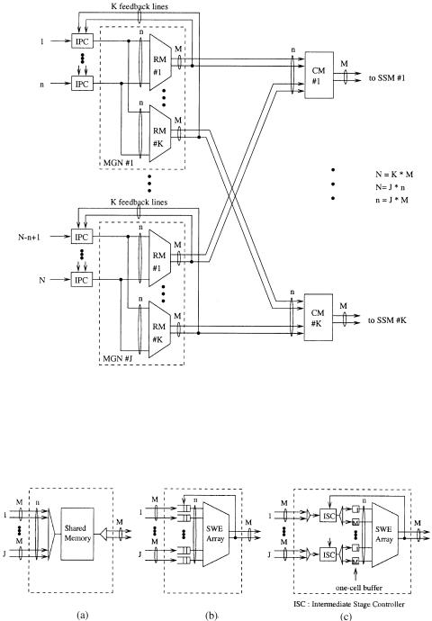
7.6.2 Buffered Multistage Concentration Network
Figure 7.20 shows a two-stage buffered multistage concentration network ŽBMCN.. As discussed in the previous section, the MMCN needs to have the feedback priority lines connected to all IPCs, which increases the interconnection complexity. This can be resolved by keeping RMs and CMs autonomous, where the FPs are extracted from the RMs rather than from the CMs. However, buffers are required in the CMs, since cells that successfully pass through the RMs and are cleared from input buffers may not pass through the CMs.
Figure 7.21 shows three ways of building the CM. Figure 7.21Ža. uses a shared-memory structure similar to the MainStreet Xpress 36190 core services
ENHANCED ABACUS SWITCH |
215 |
Fig. 7.20 A two-stage buffered multistage concentration network.
Fig. 7.21 Three ways of building the concentration module.
216 THE ABACUS SWITCH
switch w16x4 and the concentrator-based growable switch architecture w7x. Its size is limited by the memory speed constraint.
Figure 7.21Žb. shows another way to implement the CM, by using a two-dimensional SWE array and input buffers. One potential problem of having buffers at the input links of the CM is cells out of sequence. This is because after cells that belong to the same virtual connection are routed through an RM, they may be queued at different input buffers. Since the queue lengths in the buffers can be different, cells that arrive at the buffer with shorter queue lengths will be served earlier by the CM, resulting in cells out of sequence.
This out-of-sequence problem can be eliminated by time-division multiplexing cells from an RM Ž M cells., storing them in an intermediate stage controller ŽISC., and sending them sequentially to M one-cell buffers, as shown in Figure 7.21Žc.. The ISC has an internal FIFO buffer and logic circuits that handles feedback priorities as in the abacus switch. This achieves a global FIFO effect and thus maintains the cells’ sequence. Each ISC can receive up to M cells and transmit up to M cells during each cell time slot.
The key to maintaining cell sequence is to assign priority properly. At each ISC, cells are dispatched to the one-cell buffers whenever the one-cell buffers become empty and there are cells in the ISC. When a cell is dispatched to the one-cell buffer, the ISC assigns a priority value to the cell. The priority field is divided into two parts, port priority and sequence priority. The former is the more significant. The port priority field haslog 2 J bits for the J ISCs in a CM, where x denotes the smallest integer that is equal to or greater than x. The sequence priority field must have at least log 2 JM bits to ensure the cell sequence integrity to accommodate LM priority levels, as will be explained in an example later. The port priority is updated in every arbitration cycle Ži.e., in each cell slot time. in a RR fashion. The sequence priority is increased by one whenever a cell is dispatched from the ISC to a one-cell buffer. When the port priority has the highest priority level, the sequence priority is reset to zero at the beginning of the next arbitration cycle Žassuming the smaller the priority value, the higher the priority level.. This is because all cells in the one-cell buffers will be cleared at the current cycle. Using this dispatch algorithm, cells in the ISC will be delivered to the output port in sequence. The reason that the sequency priority needs to have LM levels is to accommodate the maximum number of cells that can be transmitted from an ISC between two reset operations for
the sequence priority. |
|
Figure 7.22 shows an example of |
cell’s priority assignment scheme for |
J s 3 and M s 4. The port priority |
p and sequence priority q are repre- |
sented by two numbers in w p, qx, where p s 0, 1, 2, and q s 0, 1, 2, . . . , 11. During each time slot, each ISC can receive up to four cells and transmit up to four cells. Let us consider the following case. ISC 1 receives four cells in every time slot, ISC 3 receives one cell in every time slot, and ISC 2 receives no cells.