

Книги+1 / 2013 [Chandan_Kumar_Sarkar]_Technology_CAD
.pdfMOSFET Characterization for VLSI Circuit Simulation |
283 |
7.3.4.1 Simulation Setup
For all the simulation results provided in this chapter, conventional bulk NMOS transistor has been selected. A 45-nm technology node has been selected, and the drawn channel length of the transistor is taken to be 65 nm, if not mentioned otherwise. The supply voltage is taken to be 1 V. The physical oxide thickness is 1.1 nm and the electrical oxide thickness is 1.75 nm, considering poly-depletion effect and inversion layer thickness. The substrate is uniformly doped with concentration equal to 3.24E18/cm3. The source/drain concentration is 2E20/cm3. The source/drain junction depth is 14 nm. The HSPICE simulation tool has been used to obtain all the simulation results, with BSIM4 as the compact model. The model parameters of the corresponding predictive technology model [4] have been taken for simulation purposes.
7.3.4.2 Threshold Voltage Characterization with Substrate Bias Effect
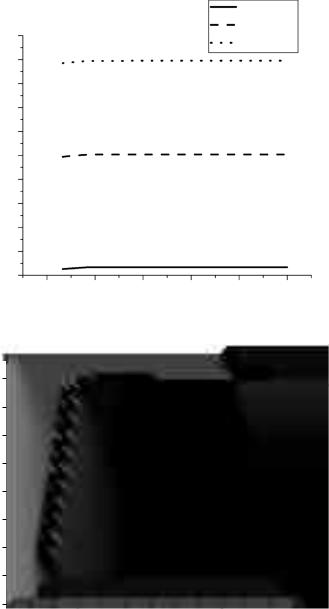
The variation of threshold voltage of a large geometry MOS transistor (W = L = 10 m) is shown in Figure 7.6(a). It is observed that the threshold voltage increases from its zero substrate bias value as the substrate voltage is increased. The value of zero substrate bias long geometry threshold voltage VT 0 as observed from Figure 7.6(a) is 0.466 V. The threshold voltage variation with substrate bias follows (7.5). Noting the values of the necessary model parameters from the model file, the theoretical curve is drawn and compared with the simulation results. It is observed that the theoretical curve closely follows the simulation results.
The variation of the substrate sensitivity of threshold voltage with the substrate bias is shown in Figure 7.6(b). The sensitivity obtained from theoretical formulation is also shown in Figure 7.6(b).
7.3.4.3 Threshold Voltage Characterization for Short Channel Transistors
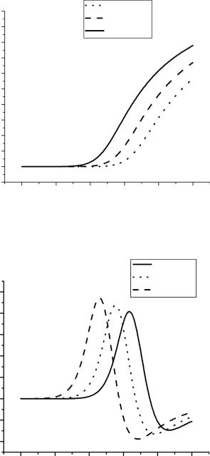
The variation of threshold voltage with channel lengths of a MOS transistor is shown in Figure 7.7(a). It is observed that as the channel length is reduced from 100 nm onwards, the threshold voltage reduces. This is referred to as the threshold voltage roll-off. The effect is more pronounced when the applied drain bias is high. This is demonstrated in Figure 7.7(b). The amount of threshold voltage roll-off as observed from the simulation results for different substrate bias and drain bias are summarized in Table 7.1. It is observed that with the increase in substrate bias, the short channel effect increases. This is easy to understand considering the fact that with the increase in substrate bias, the depletion width increases and consequently the short channel effect increases as suggested in Brew’s relation.
The DIBL effect is shown in Figure 7.8. The DIBL coefficient η is defined as
the slope of the curve (η = VT (VDS =1V)−VT (VDS =0.1V)). From simulation results, its
0.9

288 |
Technology Computer Aided Design: Simulation for VLSI MOSFET |
TABLE 7.2
Threshold Voltage Value Extracted through Different Methods
|
Extracted Value of the Threshold Voltage at |
|||
|
VDS = 50 mV. W = 10 μm L = 65 nm |
|
||
Method |
VBS = 0 V |
VBS = –0.5 V |
VBS = –1 V |
|
|
|
|
|
|
Constant current |
0.457 V |
0.559 V |
0.645 |
V |
Linear extrapolation |
0.409 V |
0.502 V |
0.583 |
V |
Second derivative |
0.462 |
0.558 |
0.636 |
|
|
|
|
|
|
in Table 7.2. For the constant current method, the constant current is taken to 1 μA, the channel width is 10 μm and the channel length is 65 nm.
7.4 I-V Characterization
Precise knowledge of the I-V characteristics of a MOS transistor is a basic requirement for a good VLSI designer. The fundamental current transport equations are introduced, followed by channel charge, mobility, and velocity saturation effects. The I-V models for long and short channel devices are derived, followed by some advanced issues.
7.4.1 Current Density Equations
The total current density is the sum of the drift current density and the diffusion current density, written as
Jn = qnµnξ + qDn |
dn |
(7.18a) |
|
|
dx |
|
|
Jp = qpµpξ − qDp |
dp |
(7.18b) |
|
dx |
|||
|
|
The total conduction current density is thus J = Jn + Jp. The diffusion coefficients Dn and Dp for electrons and holes are related to the corresponding mobilities n and p through Einstein’s relationship [5]. Thus the current densities are written as follows:
Jn = qnµnξ + kTµn |
dn |
(7.18c) |
|
|
dx |
|
|
Jp = qpµpξ − kTµp |
dp |
(7.18d) |
|
dx |
|||
|
|

290 |
Technology Computer Aided Design: Simulation for VLSI MOSFET |
|
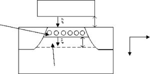
G |
|
Inversion layer |
xt |
tox |
|
– – – – – – |
y |
|
n+ S |
n+ D |
|
xb |
x |
|
Wdm |
|
|
|
B
Depletion layer
FIGURE 7.11
Inversion layer forms one capacitor with the gate and another capacitor with the body. Surface mobility is a function of the average electric fields at the top and the bottom of the inversion charge layers.
The quasi-Fermi potential VCS (y) = 0 at y = 0(source) and VCS (y) = VDS at y = L(drain).
7.4.2 Channel Inversion Charge Density
With reference to Figure 7.11, the following assumption is made. The inversion layer in the channel of a MOS transistor is a sheet of charge and there is no potential drop or band bending across the inversion layer. This is referred to as the charge sheet approximation [5]. This inversion layer forms a capacitor with the gate, the oxide being the dielectric. Also it forms another capacitor with the body, the depletion layer being the dielectric. Thus the inversion layer is coupled with both gate and substrate of the transistor. The inversion charge density in strong inversion is given by
Qinv = −[Cox (VGS − VCS (y) − VT 0 ) + Cdm (VBS − VCS (y))] |
(7.25) |
Simplification of (7.25) leads to the following expression for inversion charge density:
|
Qinv = −Cox (VGS − mVCS (y) − VT ) |
(7.26) |
|||||
where |
|
|
|
|
|||
|
m ≡ 1 + α = 1 + |
Cdm = 1 + |
3tox |
|
(7.27) |
||
Wdm |
|||||||
|
|
|
Cox |
|
|||
In (7.26), VT = VT 0 − |
Cdm |
VBS = VT 0 − αVBS = VT 0 − (m − 1)VBS |
has been taken |
||||
Cox |
|||||||
using (7.4b). |
|
|
|
|
|||

292 |
Technology Computer Aided Design: Simulation for VLSI MOSFET |
|||
The average electric field is defined as |
|
|||
|
ξeff = |
1 |
(ξxb + ξxt ) |
(7.30) |
|
|
|||
|
2 |
|
|
|
Substituting from (7.29a) and (7.29c), and after some simplifications for n+ poly-gate n-channel MOS transistor
ξeff = |
VGS + VT + 0.2V |
(7.31) |
|
6tox |
|||
|
|
Physically, ξeff means the average electric field experienced by the carriers in the inversion layer. The dependence of the surface mobility of the carriers on this average electric field and hence on the gate bias is given by the following empirical relationship [3]:
s = |
0 |
|
|
|||
1 + ( |
ξeff |
) |
υ |
(7.32) |
||
|
||||||
|
ξ0 |
|
|
|||
In (7.32), µ0 is the low field surface mobility, ν is a constant whose value is ~1.85 for electrons at the surface, and ~1.0 for holes at the surface. ξ0 is the critical electric field (~0.9 MV/cm for electrons at surface and ~0.45 MV/cm for holes at the surface). The model proposed in (7.32) fits experimental data well, but because it involves a power function, it is difficult to integrate the model in a circuit simulation program. A Taylor series expansion of (7.32) and retaining only up to three terms, the following expression for the vertical field mobility degradation model is derived:
s = |
0 |
(7.33) |
1 + UA (VGStox+VT )+ UB (VGStox+VT )2 |
In (7.33), UA and UB are two parameters, whose values are to be extracted from the experimental I-V data. The substrate bias dependence of the mobility is incorporated by introducing another parameter UC in (7.33). With this, the model becomes [6]
s = |
|
|
0 |
|
|
|
|
|
|
(7.34) |
|||
1 + (UA + UC .VBS )( |
VGS +VT |
)+ UB ( |
VGS +VT |
)2 |
|
||||||||
|
|
|
tox |
tox |
|
||||||||
µs = |
|
|
|
0 |
|
|
|
|
|
|
|
||
1 + UA ( |
VGS +VT |
)+ UB ( |
VGS +VT |
) |
2 |
|
|
|
(7.35) |
||||
|
|
|
|
||||||||||
|
(1 |
+ UCVBS ) |
|
||||||||||
tox |
tox |
|
|||||||||||