

Statistical physics (2005)
.pdf184 |
Chapter 8. Elements of Bands Theory and Crystal Conductivity |
One can notice that the band width 4A obtained for an infinite chain is only twice the value of the energy splitting for a pair of coupled sites. The reason is that, in the present model, a given site only interacts with its first neighbors and not with the more distant sites
Note : the dispersion relation (8.20) and the wave function (8.24), that we obtained under very specific hypotheses, can be generalized in the case of three-dimensional periodic solids, as can be found in basic Solid State Physics courses, like the one taught at Ecole Polytechnique.
8.3The Electron States in a Crystal
8.3.1Wave Packet of Bloch Waves
Bloch waves of the (8.21) or (8.24) type are delocalized and thus cannot describe the amplitude of probability of presence for an electron, as these waves cannot be normalized : although a localized function φ0(x) can be normed, ψk (x) spreads to infinity.
To describe an electron behavior, one has to build a packet of Bloch waves
+∞ |
|
Ψ(x, t) = −∞ g(k)eikxuk (x)e−iε(k)t/ dk |
(8.26) |
centered around a wave vector k0, of extent ∆k small with respect to π/d. From the Heisenberg uncertainty principle, the extent in x of the packet will be such that ∆x · ∆k ≥ 1, i.e., ∆x d : the Bloch wave packet is spreading over a large number of elementary cells.
8.3.2Resistance ; Mean Free Path
It can be shown that an electron described by a wave packet (8.26), in motion in a perfect infinite crystal, keeps its velocity value for ever and thus is not di used by the periodic lattice; in fact the Bloch wave solution already includes all these coherent di usions. Then there is absolutely no resistance to the electron motion or, in other words, the conductivity is infinite.
A static applied electric field E modifies the electron energy levels; the problem is complex, one should also account for the e ect of the lattice ions
which are also subjected to the action of E and interact with the electron. Experimentally one notices in a macroscopic crystal that the less its defects,
The Electron States in a Crystal |
185 |
like dislocations or impurities, the higher its conductivity. An infinite perfect three-dimensional crystal would have an infinite conductivity, a result predicted by Felix Bloch as early as 1928. (These simple considerations do not apply to the recently elaborated, low-dimensional, systems.)
The real finite conductivity of crystals arises from the discrepancies to the perfect infinite lattice : thermal motion of the ions, defects, existence of the surface. In fact in copper at low temperature one deduces from the conductivity value σ = ne2τ /m the mean time τ between two collisions and, introducing the Fermi velocity vF (see §7.1.1), one obtains a mean free path = vF τ of the order of 40 nm, that is, about 100 interatomic distances. This does show that the lattice ions are not responsible for the di usion of conduction electrons.
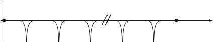
8.3.3Finite Chain, Density of States, E ective Mass
 V (x)
V (x)
0 |
d |
2d |
N d (N + 1)d |
x
Fig. 8.5 : Potential for a N -ions chain.
A real crystal is spreading over a macroscopic distance L = N d (Fig. 8.5) (the distance L is measured with an uncertainty much larger than the interatomic distance d ; one can thus always assume that L contains an integer number N of interatomic distances). Obviously, if only the coupling to the nearest neighbors is considered, for most sites there is no change with respect to the case of the infinite crystal. Thus the eigenstates of the hamiltonian for the finite crystal :
ˆ |
pˆ2 |
N |
|
+ V (x − xn) |
|
||
hcrystal = |
|
(8.27) |
|
2m |
|||
|
|
n=1 |
|
should not di er much from those of the hamiltonian (8.9) for the infinite crystal : we are going to test the Bloch function obtained for the infinite crystal as a solution for the finite case.
On the other hand, for a macroscopic dimension L the exact limit conditions do not matter much. It is possible, as in the case of the free electron model, to close the crystal on itself by superposing the sites 0 and N d and to express
186 |
Chapter 8. Elements of Bands Theory and Crystal Conductivity |
|
the periodic limit conditions of Born-Von Kármán : |
|
|
|
ψ(x + L) = ψ(x) |
(8.28) |
|
ψk(x + L) = eik(x+L)uk(x + L) = eikLψk (x) |
(8.29) |
as L contains an integer number of atoms, i.e. an integer number of atomic periods d, and uk (x) is periodic. One thus finds the same quantization condition as for a one-dimensional free particle : k = p2π/L, where p is an integer, associated with an one-dimension orbital density of states L/2π ; the corresponding three-dimensional density of states is Ω/(2π)3, where Ω is the crystal volume. These densities are doubled when one accounts for the electron spin.
The solutions of (8.27) are then |
|
|
|
|
|
|
|||||
ψk(x) = √1 |
|
|
n=1 exp iknd |
|
φ0(x |
|
nd) |
(8.30) |
|||
|
ε = ε0 |
− 2A cos kd |
· |
|
− |
|
|
||||
|
|
N |
2π |
N |
|
|
|
||||
|
|
|
|
· |
|
p integer |
|
|
|
|
|
with k = p |
|
|
|
|
|
|
|||||
|
|
|
|
|
|
|
|
|
|
|
|
L
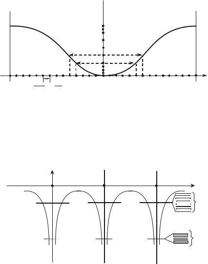
When comparing to the results (8.20) and (8.21) for the infinite crystal, one first notices that ψk(x) as given by (8.30) is normed. Moreover ε is now quan-
tized (Fig. 8.6) : to describe the first Brillouin zone −πd ≤ k < πd all the di erent states are obtained for p ranging between −N2 and + N2 − 1 (or
|
− |
2 |
|
2 |
− |
|
between |
|
N − 1 |
and |
N − 1 |
|
1 if N is odd, but because of the order of |
|
|
|
|
magnitude of N , ratio of the macroscopic distance L to the atomic one d, this does not matter much!). On this interval there are thus N possible states, i.e., as many as the number of sites. Half of the states correspond to waves propagating toward increasing x’s (k > 0), the other ones to waves propagating toward decreasing x’s.
Note that if the states are uniformly spread in k, their distribution is not uniform in energy. One defines the energy density of states D(ε) such that the number of accessible states dn, of energies between ε and ε + dε, is equal to
dn = D(ε)dε |
(8.31) |
One will note that, at one dimension, to a given value of ε correspond two
opposite values of kx, associated with distinct quantum states. By observing Fig. 8.6, it can be seen that D(ε) takes very large values at the vicinity of the band edges (ε close to ε0 ± 2A); in fact at one dimension D(ε) has a specific behavior [D(ε) diverges at the band edges, but the integral
ε
D(ε )dε |
(8.32) |
εmin
The Electron States in a Crystal |
187 |
ε(k) 
ε + 2 A
ε0 − 2 A |
|
|
0 |
|
|
−π/d |
2π |
= |
2π |
k |
|
N d |
L |
|
π/d |
||
Fig. 8.6 : Allowed states in the energy band, for a N electrons system.
remains finite]. When this model is extended to a three-dimensional system, one finds again a “quasicontinuous” set of very close accessible states, uni-
formly located in k (but not in energy), in number equal to that of the initial orbitals (it was already the case for two atoms for which we obtained the bonding and antibonding states).
|
V |
|
|
x |
|
2s |
2s |
|
band |
||
|
||
1s |
1s |
|
band |
||
|
Fig. 8.7: In a N atom crystal, to each atomic state corresponds a band that can accommodate 2N times more electrons than the initial state.
In a more realistic case, the considered atom has several energy levels (1s, 2s, 2p, ...). Each energy level gives rise to a band, wider if the atomic state lies higher in energy (Fig. 8.7). The widths of the bands originating from the deep atomic states are extremely small, one can consider that these atomic levels do not couple. On the other hand, the width of the band containing the electrons involved in the chemical bond is always of the order of several electron-volts.
188 |
Chapter 8. Elements of Bands Theory and Crystal Conductivity |
Again each band contains N times more orbital states than the initial atomic state, that is, 2N times more when the electron spin is taken into account.
The density of states in k is uniform. One defines an energy density of states D(ε) such that
|
|
L |
3 |
|
|
dn = D(ε)dε = 2 |
Å |
ã d3k at three dimensions |
(8.33) |
||
2π |
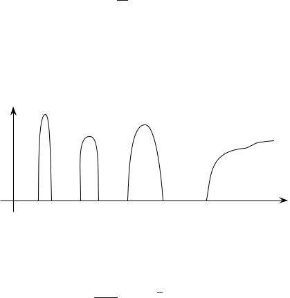
The area under the curve representing the density of states of each band is equal to 2N times the number of electrons acceptable in the initial atomic orbital : 2N for s states, 6N for p states, etc. (Fig. 8.8). The allowed bands are generally separated by forbidden bands, except when there is an overlap between the higher energy bands, which are broadened through the coupling (3s and 3p on the Fig. 8.8).
1s
D(ε) |
2p |
|
|
|
2s |
3s, 3p
ε
Fig. 8.8 : Density of states of a crystal.
It can be shown that in the vicinity of a band extremum, the tangent of the D(ε) curve is vertical. In particular, at the bottom of a band the density of state is rather similar to the one of a free electron in a box [see (6.64)], for
which we obtained D(ε) = Ω (2m)3/2√ε, m being the free electron mass.
2π2 3
Here again one will define the e ective mass in a given band, this time from the curvature of D(ε) [this mass is the same as the one in §8.2.3, introduced from the dispersion relation (8.20)]. Indeed, setting
D(ε) |
|
Ω |
(2m )3/2√ |
|
|
|
|
(8.34) |
|
|
ε |
− |
ε |
0 |
|||||
2π2 3 |
|||||||||
|
|
|
|
|
in the vicinity of ε0 at the bottom of the band is equivalent to taking for dispersion relation
ε − ε0 |
2k2 |
, i.e., |
2 |
= |
d2ε |
(8.35) |
2m |
m |
dk2 |
Statistical Physics of Solids |
189 |
The e ective mass is linked to the band width : from the dispersion relation (8.20) for instance, one obtains around k = 0
1 |
= |
2Ad2 |
(8.36) |
|
m |
2 |
|||
|
|
One can understand that the electrons of the deep bands are “very heavy,” and thus not really mobile inside the lattice, that is, they are practically localized.
Note : in non crystalline (or amorphous) solids, like amorphous silicon, the coupling between the atomic states also produces energy bands.
8.4Statistical Physics of Solids
Once the one-electron quantum states determined, one has to locate the N electrons in these states, in the framework of the independent electrons model.
8.4.1Filling of the Levels
At zero temperature, the Pauli principle dictates one to fill the levels from the lowest energy one, putting two electrons, with di erent spin states, on each orbital state until the N electrons are exhausted. We now take two examples, that of lithium (Z = 3), and that of carbon (Z = 6) crystallized into the diamond form.
In lithium, each atom brings 3 electrons, for the whole solid there are 3N electrons to be located. The 1s band is filled by 2N electrons. The complementary N electrons are filling the 2s band up to its half, until the energy ε = εF , the Fermi energy, which lies 4.7 eV above the bottom of this band. Above εF , any state is empty at T = 0 K.
When a small amount of energy is brought to the solid, for example using a voltage source of a few volts, the electrons in the 2s band in the vicinity of εF can occupy states immediately above εF , whereas 1s electrons cannot react, having no empty states in their neighborhood. This energy modification of electrons in the 2s band produces a global macroscopic reaction, expressed by an electric current, to the electric field : lithium is a metal or a conductor, the 2s band is its conduction band.
In diamond, the initial electronic states are not the 2s and 2p states of the atomic carbon but their sp3 tetrahedral hybrids (as in CH4) which separate into bonding hybrids with 4 electrons per atom (including spin) and antibon-
190 |
Chapter 8. Elements of Bands Theory and Crystal Conductivity |
ding hybrids also with 4 electrons. In the crystal, the bonding states constitute a 4N -electron band, the same is true for the antibonding states. The 4N electrons of the N atoms exactly fill the bonding band, which contains the electrons participating in the chemical bond, whence the name of valence band. The band immediately above, of antibonding type, is the conduction band. It is separated from the valence band by the band gap energy, noted Eg : Eg = 5.4 eV for diamond and at T = 0 K the conduction band is empty, the valence band having exactly accommodated all the available electrons. Under the e ect of an applied voltage of a few volts, the valence electrons cannot be excited through the forbidden band, there is no macroscopic reaction, the diamond is an insulator.
Like carbon, silicon and germanium also belong to column IV of the periodic table, they have the same crystalline structure, they are also insulators. However these latter atoms are heavier, their crystal unit cells are larger and the characteristic energies smaller : thus Eg = 1.1 eV in silicon and 0.75 eV in germanium.
Remember that a full band has no conduction, the application of an electric field producing no change of the macroscopic occupation of the levels. This is equally valid for the 1s band of the lithium metal and at zero temperature for the valence band of insulators like Si or Ge.
8.4.2Variation of Metal Resistance versus Temperature
We now are able to justify the methods and results on metals of the previous chapter, by reference to the case of lithium discussed above : their bands consist in one or several full bands, inactive under the application of an electric field, and a conduction band partly filled at zero temperature. The density of states at the bottom of this latter band is analogous to that of an electron in a box, under the condition that the free electron mass is replaced by the e ective mass at the bottom of the conduction band. Indeed we already anticipated this result when we analyzed the specific heats of copper and silver (7.2.2).
The electrical conductivity σ is related to the linear e ect of an applied field E on the conduction electrons. An elementary argument allows one to establish its expression σ = ne2τ /m , where n is the electron concentration in the conduction band, e the electron charge, τ the mean time between two collisions and m the e ective mass. A more rigorous analysis, in the framework of the transport theory, justifies this formula which is far from being obvious : the only excitable electrons are in the vicinity of the Fermi level, their velocity in the absence of electric field is vF .
The phenomenological τ term takes into account the various mechanisms
Statistical Physics of Solids |
191 |
which limit the conductivity : in fact the probabilities of these di erent independent mechanisms are additive, so that
1 |
= |
1 |
+ |
1 |
+ · · · |
(8.37) |
τ |
τvibr |
τimp |
1/τvibr corresponds to the probability of di usion by the lattice vibrations, which increases almost linearly with the temperature T , 1/τimp to the diffusion by neutral or ionized impurities, a mechanism present even at zero temperature.
Then
1 |
= ρ = |
m |
Å |
1 |
+ |
1 |
+ · · · ã |
|
σ |
ne2 |
τvibr |
τimp |
(8.38) |
ρ = ρvibr(T ) + ρimp + · · ·
Thus the resistivity terms arising from the various mechanisms add up, this is the empirical Matthiessen law, stated in the middle of the 19th century.
Consequently, the resistance of a metal increases with temperature according to a law practically linear in T , the dominating mechanism being the electron’s di usion on the lattice vibrations. This justifies the use of the platinum resistance thermometer as a secondary temperature standard between
−183◦ C and +630◦ C.
8.4.3Variation of Insulator’s Conductivity Versus Temperature; Semiconductors
a) Concentrations of Mobile Carriers in Equilibrium at Temperature T
We have just seen that at zero temperature an electric field has no e ect on an insulator, since its valence band is totally full and its conduction band empty. However there are processes to excite such systems. The two main ones are :
–an optical excitation : a photon of energy hν > Eg will promote an electron from the valence band into the conduction band. This is the absorption phenomenon, partly responsible for the color of these solids. It creates a nonequilibrium thermal situation.
–a thermal excitation : the thermal motion is also at the origin of transitions from the valence band to the conduction band. We are now going to detail this latter phenomenon, which produces a thermal equilibrium at temperature T .
192 |
Chapter 8. Elements of Bands Theory and Crystal Conductivity |
When an electron is excited from the valence band, this band then makes a transition from the state (full band) to the state (full band minus one electron), which allows one to define a quasi-particle, the “hole,” which is the lack of an electron. We already noted in chapter 7.1.1 the symmetry, due to the shape of the Fermi distribution, between the occupation factor f (ε) of energy states above µ, and the probability 1 − f (ε) of the states below µ for being empty. The following calculation will show the similarity between the electron or hole role.
The electrons inside the insulator follow the Fermi-Dirac statistics and at zero temperature the conduction band is empty and the valence band full. This means that εF lies between εv , the top of the valence band and εc, the minimum of the conduction band. At weak temperature T (kB T Eg ) one expects that the chemical potential µ still lies inside the energy band gap.
We are going to estimate n(T ), the number of electrons present at T in the conduction band and p(T ), the number of electrons missing (or holes present) in the valence band, and to deduce the energy location µ(T ) of the chemical potential. These very few carriers will be able to react to an applied electric
field E : indeed in the conduction band the electrons are very scarce at usual temperatures and they are able to find vacant states in their close neighbo-
rhood when excited by E ; in the same way the presence of several holes in
the valence band permits the valence electrons to react to E.
The volume concentration n(T ) of electrons present in the conduction band at temperature T in the solid of volume Ω is such that
Ωn(T ) = εc |
D(ε)f (ε)dε = εc |
D(ε) exp β(ε − µ) + 1 dε (8.39) |
|
εcmax |
εcmax |
1 |
|
where εc is the energy of the conduction band minimum, εcmax the energy of its maximum.
One assumes, and it will be verified at the end of the calculation, that µ is distant of this conduction band of several kB T , which leads to β(εc −µ) 1, so that one can approximate f (ε) by a Boltzmann factor. Then
ε |
|
Ωn(T ) εc cmax D(ε)e−β(ε−µ)dε |
(8.40) |
Because of the very fast exponential variation, the integrand has a significant value only if ε −εc does not exceeds a few kB T . Consequently, one can extend the upper limit of the integral to +∞, as the added contributions are absolutely negligible. Moreover, only the expression of D(ε) at the bottom of the conduction band really matters : we saw in (8.34) that an e ective mass, here mc, can be introduced, which expresses the band curvature in the vicinity of
Statistical Physics of Solids |
193 |
ε = εc. Whence
|
|
∞ |
1 |
|
|
|
|
|
|
|
|
|
|
|
||
n(T ) εc |
|
|
|
(2mc)3/2√ε − εce−β(ε−µ)dε |
(8.41) |
|||||||||||
|
2π2 3 |
|||||||||||||||
|
|
1 |
|
|
|
|
|
|
|
|
∞ |
|
|
|
|
|
= |
|
e−β(εc −µ)(2mckT )3/2 0 |
√xe−xdx |
|
||||||||||||
2π2 3 |
|
|||||||||||||||
|
|
Å |
2πmckB T |
ã |
3/2 |
|
|
εc − µ |
ã |
|
|
|
||||
= 2 |
exp |
|
|
|
(8.42) |
|||||||||||
|
|
h2 |
|
Å− kB T |
|
|
||||||||||
|
|
|
|
|
|
|
|
|
|
|||||||
In the same way one calculates the hole concentration p(T ) in the valence band, the absence of electrons at temperature T being proportional to the factor 1 − f (ε) :
εv |
|
Ωp(T ) = εvmin D(ε)[1 − f (ε)]dε |
(8.43) |
One assumes that µ is at a distance of several kB T from εv , the maximum of the valence band, of minimum εvmin. The neighborhood of εv is the only region that will intervene in the integral calculation because of the fast decrease of 1 − f (ε) e−β(µ−ε). In this region D(ε) is parabolic and is approximated by
D(ε) |
Ω |
(2mv ) |
3/2 |
√ |
|
(8.44) |
|
εv − ε |
|||||||
2π2 3 |
|
|
where mv > 0, the “hole e ective mass,” expresses the curvature of D(ε) in the neighborhood of the valence band maximum. One gets :
|
2πmv kB T |
ã |
3/2 |
|
µ − εv |
|
|
p(T ) = 2 |
exp |
|
(8.45) |
||||
h2 |
Å− kB T |
||||||
Å |
|
ã |
|||||
In the calculations between formulae (8.40) and (8.45) we did not make any assumption about the way n(T ) and p(T ) are produced. These expressions are general, as is the product of (8.42) by (8.45) :
|
Å |
2πkB T |
ã |
3 |
(mcmv )3/2 exp Å− |
Eg |
ã |
|
n(T ) · p(T ) = 4 |
|
(8.46) |
||||||
h2 |
|
kB T |
with Eg = εc − εv .
b) Pure (or Intrinsic) Semiconductor
In the case of a thermal excitation, for each electron excited into the conduction band a hole is left in the valence band. One deduces from (8.46) :
|
|
2πkB T |
ã |
3/2 |
Eg |
ã |
|
|
n(T ) = p(T ) = ni(T ) = 2 |
Å |
(mcmv )3/4 exp Å− |
(8.47) |
|||||
h2 |
2kB T |