Special Component editor fields
Inputs <number of inputs> Outputs <number of outputs>
The Component editor has two special fields for PLA devices, 'Inputs' and 'Outputs'. When you enter these values, MC7 places the specified input and output pins on the display and you must drag them into place on the shape.
Definitions
<pld type> selects the type of gate and is chosen from the following list:
Type |
Description |
|
|
PLAND |
AND array |
|
|
PLOR |
OR array |
|
|
PLNAND |
NAND array |
|
|
PLNOR |
NOR array |
|
|
PLXOR |
Exclusive OR array |
|
|
PLNXOR |
Exclusive NOR array |
|
|
PLANDC |
AND array with true and complement inputs |
|
|
PLORC |
OR array with true and complement inputs |
|
|
PLNANDC |
NAND array with true and complement inputs |
|
|
PLNORC |
NOR array with true and complement inputs |
|
|
PLXORC |
Exclusive OR array with true and complement inputs |
|
|
PLNXORC |
Exclusive NOR array with true and complement inputs |
|
|
|
Table 23-15 PLA Types |
FILE = <"file name constant" | |file name expression| >
This attribute denotes the name of a JEDEC format file in one of two formats:
File name constant enclosed in double quotes ("")
File name expression enclosed in double bars (||)
SPICE text files and libraries can use either |file name expression| or "file name constant". |file name expression| is limited to a single <text name> from a subcircuit TEXT: statement. This is the way a commercial PLD part modeled with a PLA device in a subcircuit is passed a JEDEC file name. For example:
.SUBCKT PLD24 I1 I2 O1 O2 O3 O4
+TEXT: JFILE="JD.STM"
...
U1 PLOR(2,4)
+$G_DPWR $G_DGND
+I1 I2
+O1 O2 O3 O4
+PLAMODEL
+IO_STD_PLD
+FILE=|JFILE|
Here, the PLA will use the file name assigned to JFILE. JFILE can be assigned a name when the subckt is used in a schematic or a SPICE file by supplying a FILE attribute. If is not assigned a value, JFILE will use the default value "JD.STM".
Schematic PLA devices that use the FILE attribute must use the "file name constant" option as there is no way to define a |file name expression| in a schematic.
If the FILE attribute is used, the DATA attribute is ignored. The mapping of the data in the JEDEC file is controlled by timing model parameters.
The data constant lets you create the data table in the text area or as grid text in the schematic where there is more space. It is created with a .define statement in the schematic or in the text area. The contents of the define statement are substituted for the data constant when an analysis is run. For example, consider this define statement:
.DEFINE TAB1 B$01 01 10 11 01 11 01 10 01$
If a PLA uses a data constant of TAB1, the text "B$01 01 10 11 01 11 01 10 01$" will be substituted for TAB1 when an analysis is run. 'Defines' may be used to move long definitions from any attribute VALUE field (except PART) to the text area, or just to create convenient compact constants.
<radix flag>$
This is a one character flag that defines the type of data in the DATA attribute. It is one of the following:
538 Chapter 23: Digital Devices
B Binary data
O Octal data (most significant bit =lowest address)
X Hex data (most significant bit =lowest address)
<program data>$
This text string contains data values that program the PLA. If the data value for a particular input column variable is a '0', the input column is not connected to the gate. If the data value is a '1', the input column is connected to the gate. The phrase "connected" means that a new input to the gate is created and the input (column) line is connected to the new gate input. The data values start at the zero address. For example:
U1 PLOR(3,4) |
;3-INPUT,4-OUTPUT OR TYPE PLA |
+ $G_DPWR $G_DGND |
;POWER PINS |
+ I1 I2 I3 |
;THREE INPUT PIN NAMES |
+ O1 O2 O3 O4 |
;FOUR OUTPUT PIN NAMES |
+ PLAMODEL |
;PLA TIMING MODEL NAME |
+ IO_STD_PLD |
;PLA I/O MODEL NAME |
+ DATA=B$ |
;PLA DATA PROGRAM |
+ 1 1 |
1 |
;O1 = |
I1 |
| I2 | I3 |
+ 0 |
1 |
0 |
;O2 = |
I2 |
|
+ 1 |
0 |
1 |
;O3 = |
I1 |
| I3 |
+ 0 |
0 |
1$ |
;O4 = |
I3 |
|
... |
|
|
|
|
|
True only(PLAND, PLOR, PLNAND, PLNOR, PLXOR, PLNXOR)
The zero address specifies the first input to the first output gate. The next input specifies the second input to the first output gate, and so on until all possible input connections have been specified. The process repeats for all possible input connections to the second gate until the last gate has been programmed.
True and complement(PLANDC, PLORC, PLNANDC, PLNORC, PLXORC, PLNXORC)
True and complement programming is like true only programming, except that the complement is interleaved and placed after the true. The zero address programs the first true input to the first output gate. The next input programs the connection of the first complement input to the first gate. The next input programs the connection of the second true input to the first output gate. The next input programs the connection of the second complement input to the first gate, and so on until all possible true and complement input connections have been programmed. The process is repeated for all possible true and complement input connections to the second gate until the final gate has been programmed.
The data values must be delimited by dollar signs ($). They may be separated by spaces or placed on continuation lines.
Model statement form
.MODEL <timing model name> UPLD ([model parameters])
Example
.MODEL PLD1 UPLD (TPLHMN=10ns TPLHTY=25ns TPLHMX=35ns)
|
Parameter |
Description |
Default |
|
|
|
|
|
TPLHMN |
Delay: min low to high |
0 |
|
|
|
|
|
TPLHTY |
Delay: typ low to high |
0 |
|
|
|
|
|
TPLHMX |
Delay: max low to high |
0 |
|
|
|
|
|
TPHLMN |
Delay: min high to low |
0 |
|
|
|
|
|
TPHLTY |
Delay: typ high to low |
0 |
|
|
|
|
|
TPHLMX |
Delay: max high to low |
0 |
|
|
|
|
|
OFFSET |
JEDEC file mapping: Address of first input and |
0 |
|
first gate program |
|
|
|
|
|
|
|
|
COMPOFFSET |
JEDEC file mapping: Address of complement |
1 |
|
|
of first input and first gate program |
|
|
INSCALE |
JEDEC file mapping: Amount the JEDEC file |
true only:1 |
|
address changes for each new input pin |
true & comp:2 |
|
|
|
|
|
|
|
OUTSCALE |
JEDEC file mapping: Amount the JEDEC file |
true only:<no. of inputs> |
|
address changes for each new output pin (gate) |
true & comp:2*<no. of inputs> |
|
|
|
|
|
|
Table 23-16 PLA timing model parameters
540 Chapter 23: Digital Devices
Multi-bit A/D converter
SPICE format
U<name> ADC(<bits>)
+<digital power node> <digital ground node> +<in node><ref node> <gnd node> <convert node> +<status node> <over-range node>
+<output msb node> <output lsb node> +<timing model name> <I/O model name> +[MNTYMXDLY=<delay select value>] +[IO_LEVEL=<interface subckt select value>]
Example
U10 ADC(8) $G_DPWR $G_DGND
+analog_in reference 0 convert status over B7 B6 B5 B4 B3 B2 B1 B0 +IO_STD_OC_ST
Schematic format
PART attribute <name>
Example
U10
TIMING MODEL attribute <timing model name>
Example
AF_04
I/O MODEL attribute <I/O model name>
Example
IO_AC
MNTYMXDLY attribute <delay select value>
Example 1
IO_LEVEL attribute <interface subckt select value>
Example 0
POWER NODE attribute <digital power node>
Example
$G_DPWR
GROUND NODE attribute <digital ground node>
Example
$G_DGND
Special Component editor fields
Bits <bits>
The Component editor has a special 'Bits' field for ADC devices. It lets you specify the number of output bits for the ADC. When you enter the number of bits, the system places the following pins on the display and you must drag them into place on the shape.
In Convert Ref Gnd Status
Over-range Out0
Out1
.
.
.
OutN-1
If N bits are specified there will be N output pins Out0...OutN-1.
542 Chapter 23: Digital Devices
The ADC device converts the analog voltage difference between the <in node> pin and the <gnd node> pin to an equivalent digital representation. The digital output is the binary equivalent of:
V(in node, gnd node)2<bits>
___________________
V(ref node, gnd node)
If the analog input value, V(in node, gnd node), is less than zero, then all data bits are set to '0', and over-range is set to '1'. If this value exceeds V(ref node, gnd node) then all data bits are set to '1', and the over-range pin is again set to '1'.
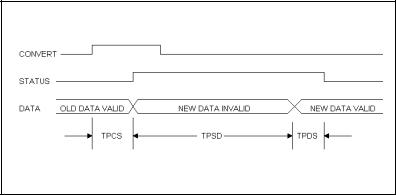
The sampling of the input voltage occurs on the rising edge of the CONVERT signal. Only one conversion is performed per rising edge.
The data output pins go to the 'X' state and the STATUS pin goes to the '1' state TPCS seconds after the rising edge of the CONVERT signal. TPSD seconds later, the data output pins change to valid data. TPDS seconds later, the STATUS pin goes to the '0' state. This timing is summarized in the diagram below:
Figure 23-2 ADC timing diagram
Model statement form
.MODEL <timing model name> UADC ([model parameters])
Example
.MODEL A1 UADC (TPCSMN=5ns TPCSTY=15ns TPCSMX=25ns)
Parameter |
Description |
Units |
|
|
|
TPCSMN |
Delay: min rising edge of Convert to rising edge of Status |
sec |
|
|
|
TPCSTY |
Delay: typ rising edge of Convert to rising edge of Status |
sec |
|
|
|
TPCSMX |
Delay: max rising edge of Convert to rising edge of Status |
sec |
|
|
|
TPSDMN |
Delay: min rising edge of Status to valid data outputs |
sec |
|
|
|
TPSDTY |
Delay: typ rising edge of Status to valid data outputs |
sec |
|
|
|
TPSDMX |
Delay: max rising edge of Status to valid data outputs |
sec |
|
|
|
TPDSMN |
Delay: min data outputs valid to falling edge of Status |
sec |
|
|
|
TPDSTY |
Delay: typ data outputs valid to falling edge of Status |
sec |
|
|
|
TPDSMX |
Delay: max data outputs valid to falling edge of Status |
sec |
|
|
|
Table 23-17 ADC timing model parameters
See the sample circuit AD16 for an example of the use of this type of device.
544 Chapter 23: Digital Devices
Multi-bit D/A converter
SPICE format
U<name> DAC(<no. of bits>)
+<digital power node> <digital ground node> +<out node> <ref node> <gnd node> +<input msb node> <input lsb node> +<timing model name> <I/O model name> +[MNTYMXDLY=<delay select value>]
+[IO_LEVEL=<interface subckt select value>]
Example
U10 DAC(8) $G_DPWR $G_DGND
+analog_out reference 0 B7 B6 B5 B4 B3 B2 B1 B0 + D0_EFF IO_STD_ST
Schematic format
PART attribute <name>
Example
U10
TIMING MODEL attribute <timing model name>
Example
DACTM
I/O MODEL attribute <I/O model name>
Example
IO_HCT
MNTYMXDLY attribute <delay select value>
Example 1
IO_LEVEL attribute <interface subckt select value>
Example 0
POWER NODE attribute <digital power node>
Example
$G_DPWR
GROUND NODE attribute <digital ground node>
Example
$G_DGND
Special Component editor fields
Bits <bits>
The Component editor has a special Bits field for DAC devices. It lets you specify the number of input bits. When you enter the number of bits, the system places the following pins on the display and you must drag them into place on the shape.
Out
Ref
Gnd
In0
In1
.
.
.
In<bits-1>
The DAC device converts the decimal value of the binary inputs to an analog voltage and impresses that voltage between the <out node> and the <gnd node>. The analog output for n input bits, bn-1,...b2, b0 is:
V(out) = V(ref,gnd) (bn-1n-1+...+b11+b00) 2-n
546 Chapter 23: Digital Devices