Digital delay ambiguity
Digital devices contain model parameters that specify a minimum, typical, and a maximum value for each timing value. The MNTYMXDLY parameter can be used to specify which of the delays to use:
MNTYMXDLY |
Meaning |
0 |
Set MNTYMXDLY = DIGMNTYMX |
1 |
Use minimum delays |
2 |
Use typical delays |
3 |
Use maximum delays |
4 |
Use worst-case (both minimum and maximum) delays |
When worst-case delays are used, the simulator produces an ambiguous region between the minimum and maximum delays that represents the period of time when the signal is changing. The signal cannot be said to be in the old state or the new state, it is merely in transition between the two states. This ambiguity region is represented by a rising or a falling state.
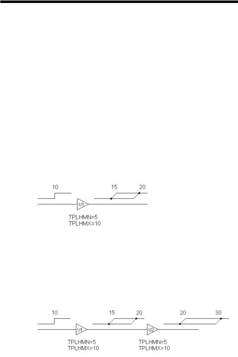
For example, in this circuit, the input changes from a '0' to a '1' at 10.
If MNTYMXDLY is 4, the resulting worst-case run produces a rising state at 15 since the minimum low to high delay is 5. The "TPLHMN=5" says that the delay is at least 5. It may be more. The "TPLHMX=10" says that the delay is at most 10. It may be less. The rising state between 15 and 20 reflects the uncertainty.
Ambiguity regions can accumulate as the signal passes through a succession of devices. For example, in this circuit the rising state ambiguity region increases as the signal passes through the two buffers.
Ambiguity can do more than just fuzz up the signal edges. It can catastrophically alter simulation results. In the circuit below, the ambiguous D input signal makes the output 'X' since there are two possible outcomes. If the clock completes its rise before the D input changes, the Q output remains '0'. If the clock completes its rise after the D input changes, the new '1' state is loaded and the Q output becomes '1'. Since there are two possible opposite states for Q depending upon when the D in-
put changes, the Q output is assigned 'X' to reflect the uncertainty.
Rising inputs do not necessarily generate 'X' results. If the CLK input samples while the D input is stable, then there is no ambiguity and the Q output is known. This is true even if the CLK input is 'R', as in this example.
498 Chapter 23: Digital Devices

Timing hazards
If the exact arrival times of the inputs to a digital device are unknown, the output may glitch or be set to 'X'. This condition is referred to as a timing hazard.
There are several types of hazards, including:
•Convergence hazards
•Cumulative ambiguity hazards
•Critical hazards
Convergence hazards
A convergence hazard occurs when two signals converge to the inputs of a gate and there is overlapping uncertainty in their arrival times, as in this example. This hazard could be represented as a 0-X-0 transition or as a 0-R-0 transition.
We represented it as a 0-R-0 transition to match the usual representation of the hazard. It should be interpreted as a possible short pulse, extending no longer than the overlap of the uncertainty portions of the two input signals.
Cumulative ambiguity hazards
Digital worst-case timing is activated when a gate's MNTYMXDLY value is set to 4. In this case the simulator adds an 'R' state between the specified minimum delay and maximum delay at each 0-1 and 0-R transition and an 'F' state between the specified minimum delay and maximum delay at each 1-0 and 1-F transition. As a signal passes through a gate with worst-case timing specified, the uncertainties of its transitions increase, as in this example:
As the signal passes through additional stages, the uncertainties can accumulate to the point where parts of the signal are ambiguous, as in this example:
At 7, the simulator attempts to schedule the 'F' state at 8 (7+1). But the '1' state is already scheduled to occur on the output at 8 (6+2). Since this is ambiguous, the simulator signals a hazard with an 'X' at 8.
Cumulative ambiguity is a particular problem with circuits that feed an inverted gate output back to its input to create an oscillator. In such cases, the MNTYMXDLY parameter of the oscillator gate should be set to something other than 4 (worst-case), to stop the signal destruction.
Critical hazards
Convergence and ambiguity hazards indicate potential problems. They may or may not cause a problem in the circuit. If the hazard causes a flip-flop or other storage device to store incorrect data, then they become critical hazards, since they will almost certainly cause a failure in the circuit.
500 Chapter 23: Digital Devices

The analog/digital interface
When a digital node and an analog node are connected together in a circuit, the program breaks the connection and inserts between the two parts an interface circuit specified by the I/O model. This interface circuit contains analog devices like resistors, capacitors, diodes, and transistors. It also contains either an analog to digital or digital to analog interface device. These devices provide the fundamental translation between the analog and digital circuits.
In addition, the simulator generates an analog power supply circuit to drive the interface circuits, as specified in the I/O model. The I/O model statement parameter, IO_LEVEL, selects one of four possible interface circuits to use. It is also possible to change the digital power supply used in the interface circuit by modifying the power supply subcircuit.
The simulator also creates additional nodes at the interface between analog and digital circuits. The creation and naming of these nodes is important to understand if you want to plot or print their values.
Nodes
There are only two types of nodes, analog and digital. When an analog node is connected to a digital node, what happens? MC7 breaks the connection and adds an interface circuit between the two parts. The interface circuit is selected from the I/O model based upon the value of the IO_LEVEL attribute. The selection is based upon the following:
Level |
Subcircuits |
Behavior |
|
|
|
1 |
AtoD1/DtoA1 |
AtoD creates R, F, and X levels |
|
|
|
2 |
AtoD2/DtoA2 |
AtoD doesn't create R, F, and X levels |
|
|
|
3 |
AtoD3/DtoA3 |
Same as Level 1 |
|
|
|
4 |
AtoD4/DtoA4 |
Same as Level 2 |
|
|
|
Table 23-2 Digital interface subcircuits
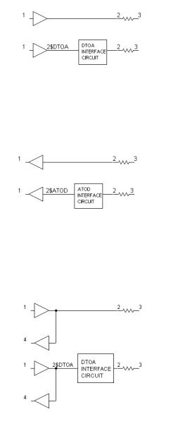
If an analog node is connected to a digital output, then a DtoA subcircuit is used. If an analog node is connected to a digital input, then an AtoD subcircuit is used. If an analog node is connected to both a digital input and a digital output then a
DtoA interface circuit is used. These cases are shown below.
When the digital node is an output node, a new digital node, 2$DTOA, is created and assigned to the digital output, and the DTOA interface circuit, specified by the I/O model statement IO_LEVEL parameter, is inserted between the new digital output node and the analog node.
When the digital node is an input node, a new digital node, 2$ATOD, is created and assigned to the digital input, and the ATOD interface circuit, specified by the I/O model statement IO_LEVEL parameter, is inserted between the new digital input node and the analog node.
When an analog node is connected to a digital node with both input and output pins connected to it, a new digital node, 2$DTOA, is created and assigned to the digital node. An interface circuit is inserted between the new digital node and the analog node.
502 Chapter 23: Digital Devices
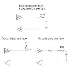
Tri-state interface caveat
When you have a digital node with input and output pins connected to it as in the last example, and the digital output comes from a tristate or open collector device, placing an analog resistor at the node will result in Z states entering the digital input. This happens because the output of the resistor does not drive the digital input, so no pullup or pulldown action can occur. To avoid this problem always follow the golden tri-state rule.
Use a digital pullup or pulldown device at tri-state nodes. Do not use an analog resistor. If you must use an analog resistor, separate the digital output from the digital input by a small value resistor.
The situation is summarized in the figure below:
Interface circuits
The I/O model parameter IO_LEVEL specifies which of the four possible interface circuits to use according to the table. If IO_LEVEL is 0, then the interface circuit will be selected by the value of the Global Settings parameter DIGIOLVL.
Level 1 Interface circuits
The level 1 interface circuits generate the intermediate logic levels (R, F, X) between the voltage ranges VILMAX and VIHMIN. A voltage that ramps smoothly from below VILMAX to above VIHMIN and back again, will generate the sequence 0, R, 1, F, 0. An X is generated if the voltage starts in the VILMAX - VIHMIN region, or the voltage reverses in the VILMAX - VIHMIN region and crosses a previously crossed threshold. The level 1 interface circuits are more accurate than level 2 circuits.
Level 2 Interface circuits
The level 2 interface circuits generate only the logic levels (0, 1). An exact switching voltage is assumed. These interface circuits are less accurate but generate no uncertain states (R, F, X) that could potentially cause simulation problems.
Level 3 and Level 4 Interface circuits. These are equivalent to Level 1 and Level 2, respectively, and are not currently used in the standard digital library.
Power supply circuits
When an analog node and a digital node are connected together, and an ATOD or DTOA interface is required, the circuit needs a power supply. The power supply is created automatically using the parameter DIGPOWER from the I/O model statement for a particular digital family, such as 7400 TTL. This parameter specifies the name of the power supply subcircuit to use. The main power supply subcircuit is called "DIGIFPWR". This subcircuit provides the voltage sources and power pins needed by the interface circuits. You can, of course, change the power supply circuit by specifying another subcircuit name, or by altering the "DIGIFPWR" subcircuit itself. We recommend leaving the original "DIGIFPWR" subcircuit intact, and cloning new versions, with related names such as "DIGIFPW1". This lets you easily revert to the old version by simply changing the DIGPOWER="DIGIFPWR" part of the I/O model statement. The
I/O model statements are located in the DIGIO.LIB model library file.
The DIGIO.LIB model library file
This file contains the I/O model statements, ATOD and DTOA interface circuits, ATOD (O device) and DTOA (N device) model statements, and power supply circuits for the entire Digital Library.
504 Chapter 23: Digital Devices

General digital primitive format
The digital device format is similar to the general SPICE component format. Both analog and digital primitives require node numbers, optional parameters, and model statements. Analog devices use at most a single model statement. Digital devices require a timing model statement and an I/O model statement.
Timing model statements define propagation delays and timing constraints. I/O model statements define the impedances, equivalent circuits, and switching times of the analog/digital interface model. The I/O model is mainly used when a digital node is connected to an analog node, but it also defines the impedances used to resolve states when device outputs of differing strengths are wired together.
Timing model statements embody data unique to each device, so most devices have unique timing model statements. The same is not true of I/O models since the interface is generally standardized for all devices within a particular digital family. For example, all 74LS devices use the same interface specification.
General format
U<name> <primitive type> [(<parameter value>*)] +<digital power node> <digital ground node> +<node>*
+<timing model name> <I/O model name> +[MNTYMXDLY=<delay select value>] +[IO_LEVEL=<interface subcircuit select value>]
Examples
U1 JKFF(1) $G_DPWR $G_DGND PRB CLB CKB J K Q QB D0_74 IO_STD U1 NOR(3) $G_DPWR $G_DGND 10 20 30 40 D0_74 IO_STD
Definition
U<name>
This is the part name.
<primitive type>
The <primitive type> specifies which of the primitive digital types, such as NAND, NOR, JKFF, or PLA, the part is.
[(<parameter value>*)]
Depending upon the <primitive type>, these are zero or more parameters representing the number of input and/or output nodes.
<digital power node> <digital ground node>
These nodes provide power to the A/D interface circuits employed when an analog node is connected to a digital node. Usually the global pins $G_DPWR and $G_DGND are used. Refer to the section, "The analog/digital interface" for more information.
<node>*
Depending upon the primitive type, these are the node names of the actual input and/or output node numbers.
<timing model name>
This name refers to a timing model statement, which specifies propagation and constraint timing values. Each model has minimum, typical, and maximum values for each timing parameter. The MNTYMXDLY device parameter selects one of the values or it lets the DIGMNTYMX select one globally.
<I/O model name>
This name refers to an I/O model statement which specifies impedance and interface circuit information for modeling the analog/digital interface.
[MNTYMXDLY=<delay select value>]
This value selects the minimum, typical, or maximum value for each timing parameter as follows:
0=Current value of DIGMNTYMX 1=Minimum
2=Typical
3=Maximum
4=Worst case. Use both minimum and maximum delays.
[IO_LEVEL=<interface subcircuit select value>]
This selects one of four interface circuits named in the I/O model. These interface circuits are used at the digital/analog interface. Refer to the I/O model topic at the end of this chapter for more information.
Timing model form
.MODEL <model name> <model type> (<model parameters>*)
Each primitive type has a unique <model type> and <model parameters>.
I/O model form
.MODEL <model name> UIO (<model parameters>*)
There is one I/O model structure that is used by all primitives.
506 Chapter 23: Digital Devices