Добавил:
Опубликованный материал нарушает ваши авторские права? Сообщите нам.
Вуз: Предмет: Файл:
Скачиваний:
68
Добавлен:
06.06.2017
Размер:
3.31 Mб
Скачать

IS(T) = IS(Tnom) e((EG/(VT•N))(T/Tnom -1))

RG(T) = RG(1 + TRG1(T - Tnom))

RD(T) = RD(1 + TRD1(T - Tnom))

RS(T) = RS(1 + TRS1(T - Tnom))

VBI(T) = VBI(T/Tnom)-3VTln((T/Tnom))-EG(Tnom)(T/Tnom)+EG(T)

CGS(T) = CGS(1+M(.0004(T-Tnom) + (1 - VBI(T)/VBI)))

CGD(T) = CGD(1+M(.0004(T-Tnom) + (1 - VBI(T)/VBI)))

Current equations level 1

Cutoff Region : Vgs VTO(T)

Id = 0

Linear and Saturation Region: (Vgs VTO(T)) > 0.0

Id=BETA(T)(1+LAMBDAVds)(VgsVTO(T))2tanh(ALPHAVds)

Current equations level 2

Cutoff Region : Vgs VTO(T)

Id = 0

Linear and Saturation Region : (Vgs - VTO(T))> 0.0

If 0< Vds< 3/ALPHA

Kt = 1 - (1 - VdsALPHA/3)3

Else

Kt = 1

Id=BETA(T)(1+LAMBDAVds)(Vgs-VTO(T))2Kt/(1+B(Vgs-VTO(T)))

Current equations level 3

Cutoff Region : Vgs VTO(T)

Id = 0

Linear and Saturation Region : (Vgs - VTO(T))> 0.0

If 0< Vds< 3/ALPHA

Kt = 1 - (1 - VdsALPHA/3)3

Else

Kt = 1

Idso = BETA(Vgs-(VTO-GAMMAVds)QKt

Id = Idso/(1+DELTAVdsIdso)

397

Capacitance equations level 1

If Vgs ≤ FCVBI(T)

Cgs = CGS/(1 - Vgs/VBI(T))M Else

Cgs = CGS(1 - FC)-(1-M)(1 - FC(1+M)+M(Vgs/VBI(T)))

If Vds ≤ FCVBI(T)

Cgd = CGD/(1 - Vgd/VBI(T))M

Else

Cgd = CGD(1 - FC)-(1-M)(1 - FC(1+M)+M(Vgd/VBI(T)))

Capacitance equations level 2 and level 3

Ve = (Vgs +Vgd + ((Vgs - Vgd)2 + ALPHA -2 )1/2 )/2

If (Ve +VTO(T) +((Ve - VTO(T))2+DELTA2)1/2)/2 < VMAX Vn = (Ve +VTO(T) +((Ve - VTO(T))2+DELTA2)1/2)/2

Else

Vn = VMAX

K1 = (1 + Ve - VTO(T))/((Ve - VTO(T))2+DELTA2)1/2)/2

K2 = (1 + (Vgs - Vgd)/((Vgs - Vgd)2+ALPHA-2)1/2)/2

K3 = (1 - (Vgs - Vgd)/((Vgs - Vgd)2+ALPHA-2)1/2)/2

Cgs = CGSK2K1/(1 - Vn/VBI(T))1/2 +CGDK3)

Cgd = CGSK3K1/(1 - Vn/VBI(T))1/2 +CGDK2)

Noise

The parasitic lead resistances, RG, RD, and RS, generate thermal noise currents.

Ig2 = 4kT / RG

Id2 = 4kT / RD

Is2 = 4kT / RS

The drain current generates a noise current.

I2 = 4kTgm2/3 + KFIdAF / Frequency where gm = ∂ Id / ∂ Vgs (at operating point)

398 Chapter 22: Analog Devices

Independent sources (V and I sources)

SPICE format

Syntax for the voltage source

Vname <plus> <minus> [[DC ] value]

+[AC magval [phaseval]]

+[PULSE v1 v2 [td [tr [tf [pw [per]]]]]]

OR [SIN vo va [f0 [td [df [ph]]]]]

OR [EXP v1 v2 [td1 [tc1 [td2 [tc2 ]]]]]

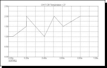
OR [PWL t1 v1 t2 v2 ...[tn , vn]] OR [SFFM vo va f0 [mi [fm]]]

Syntax for the current source

Iname <plus> <minus> [[DC ] value]

+[AC magval [phaseval]]

+[PULSE i1 i2 [td [tr [tf [pw [per]]]]]]

OR [SIN io ia [f0 [td [df [ph]]]]]

OR [EXP i1 i2 [td1 [tc1 [td2 [tc2 ]]]]]

OR [PWL t1 i1 t2 i2 ...[tn , in]] OR [SFFM io ia f0 [mi [fm]]]

The only difference between the voltage and current independent source is the use of V and I for the first character of the name.

Example

V1 10 20 DC 1 PULSE 0 1MA 12ns 8ns 110ns 240ns 500ns

Schematic format

These are the V and I sources from the Analog Primitives / Waveform Sources group of the Component menu.

PART attribute <name>

Example

V1

VALUE attribute

<value> where value is identical to the SPICE format without the name and the plus and minus node numbers.

399

Example

DC 1 PULSE 0 1MA 12ns 8ns 110ns 240ns 500ns

Equations

The equations and sample waveforms that follow are for transient analysis only. AC analysis uses AC magval (volts) and AC phaseval (degrees) to set the amplitude and phase of the small signal stimulus. TSTEP is the print interval. TSTOP is the run time. These values are obtained from the Analysis Limits dialog box. For SPICE files, MC7 obtains these values from the

.TRAN statement and copies them to the Analysis Limits dialog box.

EXP type


Name

Description

Units

Default

v1

Initialvalue

V or A

None

v2

Peak value

V or A

None

td1

Rise delay

S

0

tc1

Rise time constant

S

TSTEP

td2

Fall delay

S

td1+TSTEP

tc2

Fall time constant

S

TSTEP

The waveform value generated by the EXP option is as follows:

Time interval

Value

0 to td1

v1

td1 to td2

v1+(v2-v1)(1-e-(TIME-td1)/tc1)

td2 to TSTOP

v1+(v2-v1)((1-e-(TIME-td1)/tc1)-(1-e-(TIME-td2)/tc2))


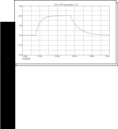
Figure 22-6 Waveform for "EXP 1 2 150n 50n 550n 100n"

400 Chapter 22: Analog Devices

PULSE type


Name

Description

Units

Default

v1

Initialvalue

V or A

None

v2

Pulse value

V or A

None

td

Delay

S

0

tr

Rise time

S

TSTEP

tf

Fall time

S

TSTEP

pw

Pulse width

S

TSTOP

per

Period

S

TSTOP

The waveform value generated by the PULSE option is as follows:

From

To

Value

0

td

v1

td

td+tr

v1

+((v2-v1)/tr)(T-td)

td+tr

td+tr+pw

v2

td+tr+pw

td+tr+pw+tf v2

+((v1-v2)/tf)(T-td-tr-pw)

td+tr+pw+tf

per

v1


where From and To are T values, and T=TIME mod per. The waveform repeats every per seconds.

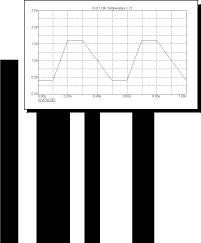
Figure 22-7 Waveform for "PULSE .4 1.6 .1u .1u .2u .1u .5u"

401

SFFM type


Name

Description

Units

Default

vo

Offset value

V or A

None

va

Peak amplitude

V or A

None

f 0

Carrier frequency

Hz

1/TSTOP

mi

Modulationindex


0

fm

Modulation freq.

Hz

1/TSTOP

The waveform value generated by the SFFM option is as follows: F = vo + vasin(2π f0T+misin(2π fmT))

where T = Transient analysis time

Figure 22-8 Waveform for "SFFM 2 1 8Meg 4 1Meg"

402 Chapter 22: Analog Devices

SIN type


Name

Description

Units

Default

vo

Offset value

V or A

None

va

Peak amplitude

V or A

None

f 0

Frequency

Hz

1/TSTOP

td

Delay

s

0

d f

Damping factor

s-1

0

ph

Phase

degrees

0

The waveform value generated by the SIN option is as follows:

From

To

Value

0


td

vo

td

TSTOP

vo+vasin(2π (f0(T-td)+ph/360))e-(T-td)•df


where T = Transient analysis time


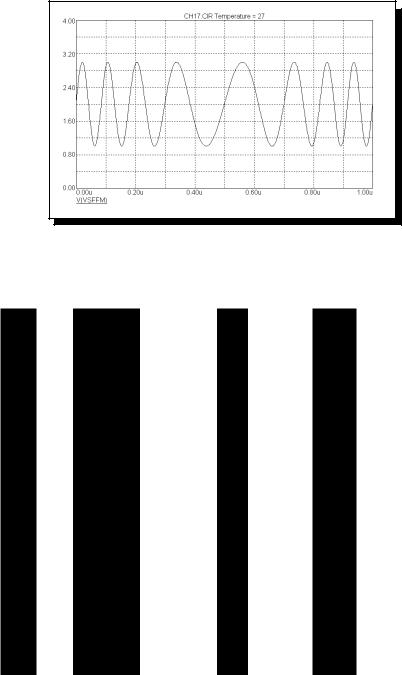
Figure 22-9 Waveform for "SIN 1 1 10Meg 100n 5E6 "

403

PWL type

General Form:

PWL

+[TIME_SCALE_FACTOR=<ts_value>]

+[VALUE_SCALE_FACTOR=<vs_value>] +(data_pairs)

where the syntax of data_pairs is: <tin>,<in>

ts_value, if present, multiplies all tin values and vs_value, if present, multiplies all in values.

Syntax for a single point on the waveform: (<tin>,<in>)

Syntax for m points on the waveform: (<tin1>,<in1>) (<tin2>,<in2>) ... (<tinm>,<inm>)

Syntax to repeat (data_pairs)* n times:

REPEAT FOR <n> (data_pairs)*

ENDREPEAT

Syntax to repeat (data_pairs)* forever:

REPEAT FOREVER (data_pairs)*

ENDREPEAT

Each data pair specifies one point on the waveform curve. Intermediate values are linearly interpolated from the table pairs.

There is no specific limit on the number of data pairs in the table. They may be added indefinitely until system memory is exhausted.

Examples:

The VALUE attribute for a 10 ns non repeating square wave: PWL (0,0) (5n,0) (5n,5) (10n,5) (10n,0)

The VALUE attribute for another 10 ns non repeating square wave: PWL TIME_SCALE_FACTOR=1n (0,0) (5,0) (5,5) (10,5) (10,0)

404 Chapter 22: Analog Devices

The VALUE attribute for a 10 ns non repeating square wave, with a high level of 5KV:

PWL VALUE_SCALE_FACTOR=1E3 (0,0) (5n,0) (5n,5) (10n,5) (10n,0)

The VALUE attribute for a 10 ns square wave, repeated 20 times:

PWL REPEAT FOR 20 (0,0) (5n,0) (5n,5) (10n,5) (10n,0) ENDREPEAT

The VALUE attribute for a 10 ns square wave, repeated forever:

PWL REPEAT FOREVER (0,0) (5n,0) (5n,5) (10n,5) (10n,0) ENDREPEAT

Here is an example of a PWL waveform:

Figure 22-10 Waveform for

"PWL 0.05u,1 0.20u,1.5 0.20u,2 0.40u,1 0.51u,2 0.61u,1.5 0.80u,2"

405

Inductor

SPICE format

Syntax

L<name> <plus> <minus> [model name] <value> [IC=<initial current>]

Examples

L1 2 3 1U

L2 7 8 110P IC=2

<plus> and <minus> are the positive and negative node numbers. Positive current flows into the plus node and out of the minus node.

Schematic format

PART attribute <name>

Examples

L5

L1

VALUE attribute

<value> [IC=<initial current>]

Examples 1U

110U IC=3 10U*(1+I(L10)/100)

FREQ attribute [fexpr]

Examples 1.2mh+5m*(1+log(F))

MODEL attribute [model name]

Examples

LM

L_MODEL

406 Chapter 22: Analog Devices

Соседние файлы в папке Micro-Cap v7.1.6
  • #
    06.06.20171.32 Кб60model.CNT
  • #
    06.06.201776.72 Кб62MODEL.HLP
  • #
    06.06.20173.72 Кб60NETHASP.INI
  • #
    06.06.2017450 б59os.dat
  • #
    06.06.2017545 б63READ.ME
  • #
    06.06.20173.31 Mб68RM.PDF
  • #
    06.06.2017226.69 Кб61setup.bmp
  • #
    06.06.201795 б59SETUP.INI
  • #
  • #
    06.06.201749 б60setup.lid
  • #
    06.06.20172.04 Mб60Standard.cmp