

Micro-Cap v7.1.6 / RM
.PDF7. Kenneth Kundert
Designers Guide to SPICE & Spectre
Kluwer Academic Publishers, 1995
8. William J. McCalla
Fundamentals of Computer-Aided Circuit Simulation
Kluwer Academic Publishers, 1988
9. Andrei Vladimiresescu and Sally Liu
The Simulation of MOS Integrated circuits using SPICE2
University of California, Berkeley Memorandum No. UCB / ERL M80/7
10.Lawrence Nagel.
SPICE2: A Computer Program to Simulate Semiconductor Circuits
University of California, Berkeley, Memorandum No. ERL - M520
11.Andrei Vladimirescu
The SPICE Book
John Wiley & Sons, Inc., First Edition, 1994. ISBN# 0-471-60926-9
Device modeling:
12.H. Statz, P. Newman, I. W. Smith, R. A. Pucel, and H. A. Haus
GaAsFET Device and Circuit Simulation in SPICE
IEEE Transactions on Electron Devices, ED - 34, 160-169 (1987)
13.Graeme R. Boyle, Barry M. Cohn, Donald O. Petersen, and James E. Solomon
Macromodeling of Integrated Circuit Operational Amplifiers
IEEE Journal of Solid-State Circuits, Vol. SCV-9 No. 6 (1974)
14.W.R Curtice
A MESFET model for use in the design of GaAs integrated circuits
IEEE Transactions on Microwave Theory and Techniques MTT - 28,448-456 (1980)
15.Ian Getreu
Modeling the Bipolar Transistor
Tektronix, 1979
367
16.MOSPOWER Applications copyright 1984, Signetics, Inc.
17.Bing Jay Sheu
MOS Transistor Modeling and characterization for Circuit Simulation
University of California, Berkeley Memo No. UCB / ERL M85/85
18.Yannis P. Tsividis
Operation and Modeling of the MOS Transistor
McGraw-Hill, 1987
19.Paolo Antognetti, and Giuseppe Massobrio
Semiconductor Device Modeling with SPICE.
McGraw-Hill, 1988
20.D. C. Jiles, and D. L. Atherton Theory of Ferromagnetic Hysteresis
Journal of Magnetism and Magnetic Materials, 61, 48 (1986)
21.SallyLiu
A Unified CAD Model for MOSFETs
University of California, Berkeley Memorandum No. UCB / ERL M81/31
22.Y. Cheng, M. Chan, K. Hui, M. Jeng, Z. Liu, J. Huang, K. Chen, J. Chen, R. Tu, P. Ko, C. Hu
BSIM3v3.1 Manual
Department of Electrical Engineering and Computer Sciences University of California, Berkeley
23.Daniel Foty
MOSFET Modeling with SPICE Principles and Practice
Prentice Hall, First Edition, 1997. ISBN# 0-13-227935-5
Filters:
24.Lawrence P. Huelsman
Active and Passive Filter Design, An Introduction
McGraw-Hill, 1993
368 Chapter 22: Analog Devices
25.Kendall L. Su
Analog Filters
Chapman & Hall, 1996
26.Arthur B. Williams
Electronic Filter Design Handbook
McGraw-Hill, 1981
Switched-Mode Power Supply Circuits:
27.Christophe Basso
Switch-Mode Power Supply SPICE Simulation Cookbook
McGraw-Hill, 2001
28.Steven M. Sandler
SMPS Simulation with SPICE 3
McGraw Hill, First Edition, 1997. ISBN# 0-07-913227-8
SPICE Modeling:
29.Ron Kielkowski
SPICE - Practical Device Modeling
McGraw Hill 1995. ISBN# 0-07-911524-1
30.Ron Kielkowski
Inside SPICE - Overcoming the Obstacles of Circuit Simulation
McGraw Hill 1993. ISBN# 0-07-911525-X
31.Connelly and Choi
Macromodeling with SPICE
Prentice Hall 1992. ISBN# 0-13-544941-3
RF Circuits:
27.Vendelin, Pavio, and Rhoda
Microwave Circuit Design
Wiley-Interscience, 1990
369

Battery
Schematic format
PART attribute <name>
Example
V1
VALUE attribute <value>
Examples 10
5.5V
The battery produces a constant DC voltage. It is implemented internally as the simplest form of SPICE independent voltage source. Its main virtue lies in its simplicity.
The battery provides simple constant voltage values. If you need a voltage source that is dependent on other circuit variables or time, use one of the dependent sources or the function source (NFV).
370 Chapter 22: Analog Devices

Bipolar transistor
SPICE format
Syntax
Q<name> <collector> <base> <emitter> [substrate] +<model name> [area] [OFF] [IC=<vbe>[,vce]]
Examples
Q1 5 7 9 2N3904 1 OFF IC=0.65,0.35
Q2 5 7 9 20 2N3904 2.0
Q3 C 20 OUT [SUBS] 2N3904
Schematic format
PART attribute <name>
Examples
Q1
BB1
VALUE attribute
[area] [OFF] [IC=<vbe>[,vce]]
Example
1.5 OFF IC=0.65,0.35
MODEL attribute <model name>
Example 2N2222A
The initialization, 'IC=<vbe>[,vce]', assigns initial voltages to the junctions in transient analysis if no operating point is done (or if the UIC flag is set). Area multiplies or divides parameters as shown in the model parameters table. The OFF keyword forces the BJT off for the first iteration of the operating point.
Model statement forms
.MODEL <model name> NPN ([model parameters])
.MODEL <model name> PNP ([model parameters])
.MODEL <model name> LPNP ([model parameters])
371

Examples
.MODEL Q1 NPN (IS=1E-15 BF=55 TR=.5N)
.MODEL Q2 PNP (BF=245 VAF=50 IS=1E-16)
.MODEL Q3 LPNP (BF=5 IS=1E-17)
Name |
Parameter |
Unit/s |
|
Default Area |
|
IS |
Saturation current |
A |
|
1E-16 |
* |
BF |
Ideal maximum forward beta |
|
|
100.0 |
|
NF |
Forward current emission coefficient |
|
|
1.00 |
|
VAF |
Forward Early voltage |
V |
|
∞ |
|
IKF |
BF high-current roll-off corner |
A |
|
∞ |
* |
ISE |
BE leakage saturation current |
A |
|
0.00 |
* |
NE |
BE leakage emission coefficient |
|
|
1.50 |
|
BR |
Ideal maximum reverse beta |
|
|
1.00 |
|
NR |
Reverse current emission coefficient |
|
|
1.00 |
|
VAR |
Reverse Early voltage |
V |
|
∞ |
|
IKR |
BR high-current roll-off corner |
A |
|
∞ |
* |
ISC |
BC leakage saturation current |
A |
|
0.00 |
* |
NC |
BC leakage emission coefficient |
|
|
2.00 |
|
NK |
High current rolloff coefficient |
|
|
0.50 |
|
ISS |
Substrate pn saturation current |
A |
|
0.00 |
* |
NS |
Substrate pn emission coefficient |
Ω |
|
1.00 |
|
RC |
Collector resistance |
|
0.00 |
/ |
|
RE |
Emitter resistance |
Ω |
|
0.00 |
/ |
RB |
Zero-bias base resistance |
Ω |
|
0.00 |
/ |
IRB |
Current where RB falls by half |
Α |
∞ |
|
* |
RBM |
Minimum RB at high currents |
Ω |
|
RB |
/ |
TF |
Ideal forward transit time |
S |
|
0.00 |
|
TR |
Ideal reverse transit time |
S |
|
0.00 |
|
XCJC |
Fraction of BC dep. cap. to internal base |
|
|
1.00 |
|
MJC |
BC junction grading coefficient |
|
|
0.33 |
|
VJC |
BC junction built-in potential |
V |
|
0.75 |
|
CJC |
BC zero-bias depletion capacitance |
F |
|
0.00 |
* |
MJE |
BE junction grading coefficient |
|
|
0.33 |
|
VJE |
BEjunctionbuilt-inpotential |
V |
|
0.75 |
|
CJE |
BE zero-bias depletion capacitance |
F |
|
0.00 |
* |
MJS |
CS junction grading coefficient |
|
|
0.00 |
|
VJS |
CSjunctionbuilt-inpotential |
V |
|
0.75 |
|
CJS |
CS junction zero-bias capacitance |
F |
|
0.00 |
* |
VTF |
Transit time dependence on VBC |
V |
|
∞ |
|
ITF |
Transit time dependence on IC |
A |
|
0.00 |
* |
XTF |
Transit time bias dependence coefficient |
|
|
0.00 |
|
PTF |
Excess phase |
|
|
0.00 |
|
XTB |
Temperature coefficient for betas |
|
|
0.00 |
|
372 Chapter 22: Analog Devices
Name |
Parameter |
Units |
Default Area |
EG |
Energy gap |
eV |
1.11 |
XTI |
Saturation current temperature exponent |
|
3.00 |
KF |
Flicker-noise coefficient |
0.00 |
|
AF |
Flicker-noise exponent |
|
1.00 |
FC |
Forward-bias depletion coefficient |
|
0.50 |
T_MEASURED |
Measured temperature |
°C |
|
|
T_ABS |
|
Absolute temperature |
°C |
|
T_REL_GLOBAL |
Relative to current temperature |
°C |
|
|
T_REL_LOCAL |
Relative to AKO temperature |
°C |
|
|
TRE1 |
RE linear temperature coefficient |
°C-1 |
0.00 |
|
TRE2 |
RE quadratic temperature coefficient |
°C-2 |
0.00 |
|
TRB1 |
RB linear temperature coefficient |
°C-1 |
0.00 |
|
TRB2 |
RB quadratic temperature coefficient |
°C-2 |
0.00 |
|
TRM1 |
RBM linear temperature coefficient |
°C-1 |
0.00 |
|
TRM2 |
RBM quadratic temperature coefficient |
°C-2 |
0.00 |
|
TRC1 |
RC linear temperature coefficient |
°C-1 |
0.00 |
|
TRC2 |
RC quadratic temperature coefficient |
°C-2 |
0.00 |
|
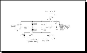
BJT model equations
Figure 22-1 Bipolar transistor model
Definitions
The model parameters IS, IKF, ISE, IKR, ISC, ISS, IRB, CJC, CJE, CJS, and ITF are multiplied by [area] and the model parameters RC, RE, RB, and RBM are divided by [area] prior to their use in the equations below.
T is the device operating temperature and Tnom is the temperature at which the model parameters are measured. Both are expressed in degrees Kelvin. T is set to
373
the analysis temperature from the Analysis Limits dialog box. TNOM is determined by the Global Settings TNOM value, which can be overridden with a .OPTIONS statement. T and Tnom may both be customized for each model by specifying the parameters T_MEASURED, T_ABS, T_REL_GLOBAL, and T_REL_LOCAL. For more details on how device operating temperatures and Tnom temperatures are calculated, see the .MODEL section of Chapter 20, "Command Statements".
The substrate node is optional and if not specified, is connected to ground. If the substrate node is specified and is an alphanumeric name, it must be enclosed in square brackets.
The model types NPN and PNP are used for vertical transistor structures and the LPNP is used for lateral PNP structures. The isolation diode DJ and capacitance CJ are connected from the substrate node to the internal collector node for NPN and PNP model types, and from the substrate node to the internal base node for the LPNP model type.
When adding new four terminal BJT components to the Component library, use NPN4 or PNP4 for the Definition field.
When a PNP4 component is placed in a schematic, the circuit is issued an LPNP model statement. If you want a vertical PNP4, change the LPNP to PNP.
VT = k•T/q
VBE = Internal base to emitter voltage
VBC = Internal base to collector voltage
VCS = Internal collector to substrate voltage
In general, X(T) = Temperature adjusted value of parameter X
Temperature effects
EG(T) = 1.16 - .000702•T2/(T+1108)
IS(T) = IS•e((T/Tnom-1)•EG/(VT))•(T/Tnom)(XTI)
ISE(T) = (ISE/(T/Tnom)XTB)•e((T/Tnom-1)•EG/(NE•VT))•(T/Tnom)(XTI/NE)
ISC(T) = (ISC/(T/Tnom)XTB)•e((T/Tnom-1)•EG/(NC•VT))•(T/Tnom)(XTI/NC)
BF(T) = BF•(T/Tnom)XTB
BR(T) = BR•(T/Tnom)XTB
VJE(T) = VJE•(T/Tnom)-3•VT•ln((T/Tnom))-EG(Tnom)•(T/Tnom)+EG(T)
VJC(T) = VJC•(T/Tnom)-3•VT•ln((T/Tnom))-EG(Tnom)•(T/Tnom)+EG(T)
VJS(T) = VJS•(T/Tnom)-3•VT•ln((T/Tnom))-EG(Tnom)•(T/Tnom)+EG(T)
CJE(T) = CJE•(1+MJE•(.0004•(T-Tnom) + (1 - VJE(T)/VJE)))
CJC(T) = CJC•(1+MJC•(.0004•(T-Tnom) + (1 -VJC(T)/VJC)))
374 Chapter 22: Analog Devices

CJS(T) = CJS•(1+MJS•(.0004•(T-Tnom) + (1 - VJS(T)/VJS)))
Current equations
Q1 = 1/ (1 - VBC/VAF - VBE/VAR)
Q2 = IS(T)•(e(VBE/(NF•VT))-1)/IKF + IS(T)•(e(VBC/(NR•VT))-1)/IKR
QB = Q1•(1+(1+4•Q2)0.5 ) / 2
Current source value
ICT = IS(T)•(e(VBE/(NF•VT))-1)/QB - IS(T)•(e(VBC/(NR•VT))-1)/QB
Base emitter diode current
IBE = ISE(T)•(e(VBE/(NE•VT))-1)+IS(T)•(e(VBE/(NF•VT))-1)/BF(T)
Base collector diode current
IBC = ISC(T)•(e(VBC/(NC•VT))-1)+IS(T)•(e(VBC/(NR•VT))-1)/QB/BR(T)
Base terminal current
IB = IBE + IBC
IB = IS(T)•(e(VBE/(NF•VT))-1)/BF(T)+ISE(T)•(e(VBE/(NE•VT))-1)+
IS(T)•(e(VBC/(NR•VT))-1)/BR(T)+ISC(T)•(e(VBC/(NC•VT))-1)
Collector terminal current
IC = IS(T)•(e(VBE/(NF•VT))- e(VBC/(NR•VT)))/QB
- IS(T)•(e(VBC/(NR•VT))-1)/BR(T)- ISC(T)•(e(VBC/(NC•VT)) -1)
Emitter terminal current
IE = IS(T)•(e(VBE/(NF•VT))-e(VBC/(NR•VT)))/QB
+IS(T)•(e(VBE/(NF•VT))-1)/BF(T)+ISE(T)•(e(VBE/(NE•VT))-1)
Capacitance equations
Base emitter capacitance
GBE = base emitter conductance = ð(IBE) / ð(VBE)
If VBE ≤ FC•VJE(T)
CBE1 =CJE(T)•(1 - VBE/VJE(T))-MJE
Else
CBE1 = CJE(T)•(1 - FC)-(1+MJE) • (1 - FC•(1+MJE)+MJE•VBE/VJE(T))
R = IS(T)•(e(VBE/(NF•VT))-1)/(IS(T)•(e(VBE/(NF•VT))-1)+ITF)
CBE2 = GBE•TF•(1+XTF•(3•R2-2•R3)•e(VBC/(1.44•VTF)))
CBE = CBE1+CBE2
375

Base collector capacitances
GBC = base collector conductance = ð(IBC) / ð(VBC)
If VBC ≤ FC•VJC(T)
C = CJC(T)•(1 - VBC/VJC(T))-MJC
Else
C = CJC(T)•(1 - FC)-(1+MJC) • (1 - FC•(1+MJC)+MJC•VBC/VJC(T))
CJX = C•(1- XCJC)
CBC = GBC•TR + XCJC•C
Collector substrate capacitance
If VCS ≤ 0
CJ = CJS(T)•(1 - VCS/VJS(T))-MJS
Else
CJ = CJS(T)•(1 - FC)-(1+MJS) • (1 - FC•(1+MJS)+MJS•VCS/VJS(T))
Noise
RE, RB, and RC generate thermal noise currents.
Ie2 = (4 • k • T) / RE
Ib2 = (4 • k • T) / RB
Ic2 = (4 • k • T ) / RC
Both the collector and base currents generate frequency-dependent flicker and shot noise currents.
Ic2 = 2 • q • Ic + KF • ICBAF / Frequency
Ib2 = 2 • q • Ib + KF • IBEAF / Frequency
where
KF is the flicker noise coefficient AF is the flicker noise exponent
376 Chapter 22: Analog Devices