![](/user_photo/1393_G1Syr.jpg)
- •Copyright Notice
- •Contents
- •Introduction to PCB Artist
- •Introduction to the Tutorial
- •Additional Help
- •System Requirements
- •Installation
- •Removing the Software
- •Starting PCB Artist
- •The PCB Artist Desktop
- •Toolbars
- •Cancelling Commands
- •Shortcut Keys
- •Units
- •Grids
- •Snapping to Grid
- •Shortcut Menus
- •Undo/Redo
- •Properties of items
- •Status Bar
- •Dockable Windows and Browsers
- •Schematic Design Tutorial
- •Starting a New Schematic
- •Adding Components
- •Placing Components
- •Adding Connections
- •Adding Power & Ground Symbols
- •Adding Connectors
- •Naming Connections
- •Your Schematic is Finished
- •Converting the Schematic to PCB
- •Starting a New PCB Design
- •The New PCB Wizard
- •Schematic Design Completed
- •Getting Started with the Design
- •Converting the Schematic to PCB
- •Changing the Number of Layers
- •Creating a Board Outline Interactively
- •Deleting an existing board outline
- •Adding a new board outline
- •Placing Components
- •Routing the Design
- •Automatic Routing
- •Unrouting the design
- •Manual Routing
- •Summary of the basic modes of routing
- •Picking in tight areas
- •Pouring Copper into Areas
- •Checking the Design Integrity
- •Design Rules Checking
- •Viewing Power Plane Layers
- •Reports, Part Lists and Net Lists
- •Manufacturing the PCB
![](/html/1393/253/html_p4XN27XnHy.TxXp/htmlconvd-b4Kp6k50x1.jpg)
50 Chapter 4 – PCB Design Editor
Checking the Design Integrity
Various checks are available in both the Schematic and PCB editors on the Tools menu. This is used to compare and verify designs and make changes in the PCB so that they are both insync with each other at all times.
To check the designs
You can use the Consistency Check option from the Schematic < -- > PCB > menu on the Tools menu at any time. By default, the file used for the comparison will be the same name as that used for the Schematic (or PCB design if running from the Schematic editor).
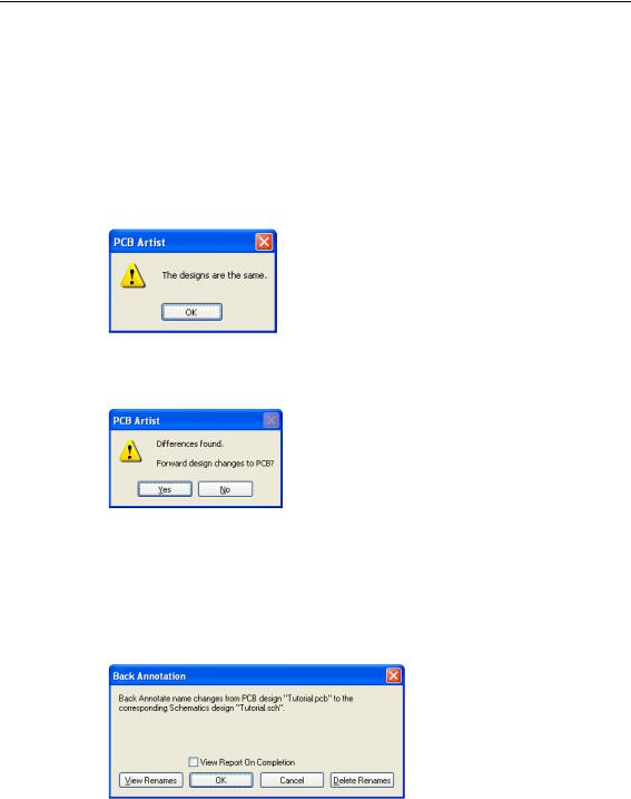
When run, if there are no differences, the following dialog is displayed:
If differences are found, Notepad will be run to view a detailed report. The report will give you a list of changes that would have to be made to the PCB in order to make it match the schematic (the schematic always being the ‘master’). You can then perform these changes automatically by selecting the Yes button on the dialog.
Run this option on our tutorial design, there should be no differences. If there are, click the Yes button and make the changes.
To back annotate name changes to the Schematic
Back annotation changes can be made in the PCB, and these can be passed back to the schematic also using the Back Annotation option from the Tools menu. When run, it will report and allow you to perform any back annotation changes to the Schematic that are ‘pending’.