


32 Chapter 2 – Schematic Capture Editor
Your Schematic is Finished
The schematic design is complete. You may wish to print it to check it, use the Print option from the File menu.
The next stage is to convert the design into the PCB design environment. To do this, move onto the next chapter Chapter 3. - Converting Your Schematic To PCB

Chapter 3 – Converting your Schematic to PCB 33
Chapter 3. Converting Your Schematic To PCB
Converting the Schematic to PCB
If you created a Schematic in PCB Artist, the final process before starting on the PCB design itself is to translate the Schematic design into the PCB design editor.
When you are in a position where you wish to go-ahead with this translation you should select Schematic <- - > PCB > and use the Translate To PCB option from the Tools menu.
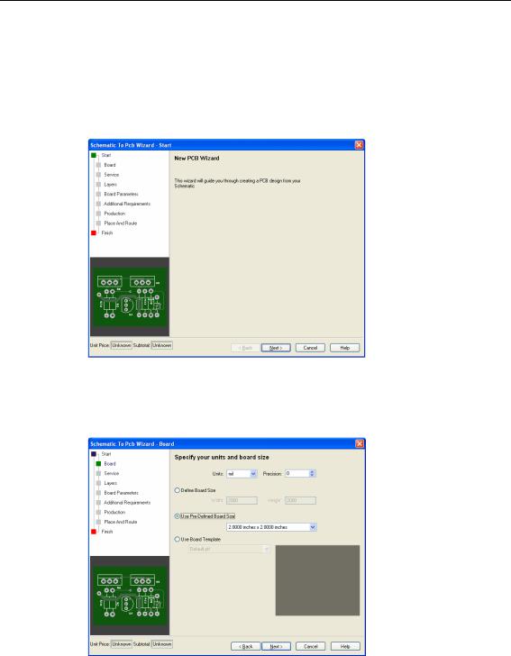
This will display the New Pcb wizard.
Starting a New PCB Design
If you intend starting a new PCB design without using a Schematic design first (which you are quite able to do), from the File menu select New and check the New PCB Design radio button. Click the OK button and this will start the New PCB Wizard.
34 Chapter 3 – Converting your Schematic to PCB
The New PCB Wizard
This wizard is a set of dialogs which you step through in sequence to define aspects of your design in the PCB design editor. The online help is available for each page by pressing the <F1> key at any time.
Click Next > to move onto the next page. You can also click the page name you require in the list at the top left hand side of the page but is recommended to work through the wizard pages in sequence.
The Board page allows you to define the Units used in the design and the board size. If your manufacturer has supplied some template designs with commonly used board outlines, they will be presented in the Use Board Template list for you to choose from.
For the tutorial, select the Use Pre-Defined Board Size radio button and select 2.000 inches x 2.000 inches from the list. Click Next >
The Service page is used to select a named service. This is used to predefine ‘standard’ services that we provide or to customize the service required.

Chapter 3 – Converting your Schematic to PCB 35
Using a Standard Service will enable you to place an order directly using the Submit Order option. If defining a Custom service, you will have to get a quote from the Submit Order dialog before proceeding with the order.
The Layers page is used to define how many layers the design contains and how they look when manufactured. Remember that the number of layers used will also be a factor when the cost of the board is calculated.
Leave the setting of 2 Layer Board for Electrical Layers and all other settings for now.
If you had selected a greater number of layers than 2, 4 or 6 for example, you would need to also select how the inner layers would be used. If you wish to use the inner layers as power planes, check the Powerplane Layers check boxes and enter the net name associated with that layer. For the example below, we have selected both Layers 2 and 3 and have assigned them plane net names of GND and +15V respectively.

36 Chapter 3 – Converting your Schematic to PCB
Click the Next > button to continue.
The Board Parameters page is used to define the material used to manufacture the final PCB.
Use this as it is for now. Click the Next > button.
Additional Requirements is used to tell the manufacturer about any special requirements using the notes window into which you can type your message.
You can specify Electrical Testing and Component Assembly as ‘cost’ options.

Chapter 3 – Converting your Schematic to PCB 37
The Production page is used to specify how fast you require the board and the production quality and quantity. The cost of the PCBs, if available, is shown in the cost box.
The Place And Route page is shown if you are transferring a schematic. It allows you to tell the PCB editor what to do with the parts and nets once in the PCB design. You can opt to place components and route them automatically, or just leave the placement and routing for you to do manually.
For the tutorial we will change the settings to allow you to do the placement and routing manually once in the PCB design editor. Select the Arrange Around the Board button.
Click the Next > button.
The Finish page allows you to give your PCB design a name and to save it to a file in a chosen location.
Click the Save the PCB Design To File check box and type in a suitable name. You should give it the same name as the schematic, but with the .pcb file extension Tutorial.pcb
Click the Finish button.