

46 Chapter 4 – PCB Design Editor
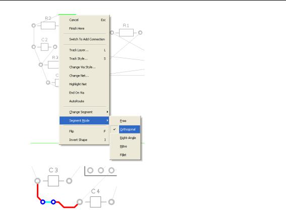
This mode can be changed by accessing the routing mode during routing. Select the Segment Mode> from the shortcut menu and choose the mode from the choice of five available.
On our example design, the routing may now look like this using the Mitre mode.
Picking in tight areas
When attempting to select items within a dense area of the design or where multiple connections cross each other for example, it is not always easy to pick the item required at the first attempt. Under these circumstances PCB Artist has a system of picking that 'cycles' through items adjacent to it until you select the item required. Once selected, an action may be made on that item, Properties for example.
The shortcut key used for the command Select Next is defined as N for Next.
To try this, click on a pad that has a track attached to it, the pad (or track) is selected. Now click <N> and the track (or pad) will be selected. Depending on how close it is to other design items, the component outline and the whole component may also be selected at each click of <N> is made.
Pouring Copper into Areas
Copper Pour is used to flood areas of a PCB layout with copper, usually connected to a nominated signal through ‘thermal’ connections, typically Ground (GND) or VCC. This facility will then create voids around tracks, component pads, vias and other electrical obstacles.
For this we have the Add Copper Pour Area and Pour Copper options.
If a copper area is to be inserted without the need for voids around unconnected tracks, components or pads, the Add Copper option can be used.

Chapter 4 – PCB Design Editor 47
The principle of this facility is to insert a Copper Pour Area and ‘pour’ the copper into this area.
To create a Copper Pour Area
From the Add menu, select Copper Pour Area> Rectangle Other Pour Area options are available for adding different shapes. We will add the pour area to the Top Copper layer. pour areas and poured copper can be added to any electrical layer. To change layers, select the pour area and click L followed by <Enter> as we did when editing tracks.
The shape can be created on the design and the pour area can be drawn protruding outside the board outline. PCB Artist will pour the copper using the Spacing rules and rules defined for the Pour area.
Following the picture below of our example, draw in a basic rectangle pour area shape, this is shown in black in the top left hand side of the design:
For this example you will see how easy it is to add a poured copper area. Right click on the pour area.
From the shortcut menu select Pour Copper.

48 Chapter 4 – PCB Design Editor
A dialog is displayed from where you can select parameters for the poured area, such as the net name association and thermal connections etc.
For this exercise, leave the Net Name blank and simply click OK.
Notice that the poured copper has obeyed the Spacing rules of all defined items to copper including Board to Shape rules.
To remove poured copper from a copper pour area
To remove a poured copper area (including any thermal spokes), simply select the area outline and select Clear Copper from the shortcut menu. This removes the copper but not the Copper Pour area.

Chapter 4 – PCB Design Editor 49
When using poured copper remember you shouldn’t use Delete but should always use Clear
Copper. Copper Pour Areas can be modified at any time and the area re-poured using the option from the shortcut menu. If you wish to completely remove the copper and area, you must use Clear Copper first and then delete the area afterwards using the Delete key.
To make the copper Pour Area intelligent
There are more facets to the poured copper than we have discussed above. The poured copper can also have a net name associated with it so that when poured, pads are connected via thermal spokes to the copper itself. To do this, select the pour area and from the shortcut menu select Add To Net. Select the net name required from the list and then re-pour the copper. Try it again using 0V as the net name and click OK.
Using the Thermal Pads check box and the Spokes settings, the style of how the copper is connected to pads can be defined.
Copper Pour Areas will not appear on your manufactured boards, they provide the system with an intelligent area into which the copper can be poured.