12.5 Quantum Structures and Single-Electron Devices (EE) 619
12.5.2 Tunneling and the Landauer Equation (EE)
Metal-Barrier-Metal Tunneling (EE)
We start by considering tunneling through a barrier as suggested in Fig. 12.6. We assume each (identical) metal is in local equilibrium with a chemical potential μ. Due to an applied external potential difference φ, we assume the chemical potential is shifted down by −eφ/2 (e > 0) for metal 1 and up by eφ/2 for metal 2 (see Fig. 12.7).
|
|
|
y |
|
|
|
|
|
|
|
|
|
Metal 1 |
z |
|
|
x |
Metal 2 |
|
|
|
|
|
Barrier |
|
|
|
|
|
|
|
Fig. 12.6. Schematic diagram for barrier tunneling
 Energy
E
μ + e2ϕ
μ
μ − e2ϕ
 barrier
x
Fig. 12.7. Tunneling sketch
We consider an electron of energy E and assume it tunnels through the barrier without changing energy. We write its energy as (with W defined by the equation and assuming for simplicity the same effective mass in all directions)
E =W + E + C = |
2kx2 |
+ |
2 |
(k 2 |
+ k 2 ) + C , |
|
|
|| |
2m |
2m |
y |
z |
|
|
|
where C is a constant that determines the bottom of the conduction band and m*, assumed constant, is the effective mass. We assume, for this case, that the transmission coefficient T across the barrier depends only on W, T = T(W). We insert a factor of 2 for the spin and consider electron flow in the ±x directions. With φ = 0, let the chemical potential in each metal be μ and the Fermi function
f (E, μ) = 1 . exp[(E − μ) / kT ] +1
620 12 Current Topics in Solid Condensed–Matter Physics
Notice μ → μ – eφ/2 is the same as E → E + eφ/2. Then the current density J is (considering current flowing each way, ±x)
dJ = −2evx[ f (E + eϕ / 2, μ)(1− f (E − eϕ / 2, μ)) |
d3k |
|
|
− f (E − eϕ / 2, μ)(1− f (E + eϕ / 2, μ))]T (W ) |
. |
|
(2π)3 |
|
|
|
|
|
|
|
|
|
|
|
|
|
|
|
|
|
|
Since |
|
|
|
|
|
|
|
|
|
|
|
|
|
|
|
|
|
|
|
|
|
|
|
|
|
|
vx = |
1 |
|
|
∂E |
, |
|
|
|
|
|
|
|
|
|
|
|
|
∂kx |
|
|
|
|
|
|
|
|
|
|
|
|
|
|
|
|
|
|
|
|
then |
|
|
|
|
|
|
|
|
|
|
|
|
|
|
|
|
|
|
|
|
|
|
|
|
|
|
vxdkx = |
1 |
dE . |
|
|
|
|
|
|
|
|
|
|
|
|
|
|
|
|
Also d3k = dkxdkydkz and since |
|
|
|
|
|
|
|
|
|
|
|
|
|
|
|
|
|
2k 2 |
|
|
|
|
|
|
|
|
|
|
|
|
W = E − |
|| |
−C |
with |
(k 2 |
= k 2 |
+ k 2 ) , |
|
|
|
|
|
|
|
|
|
|
|
2m |
|
|
|
|
|
|| |
y |
z |
|
|
|
|
|
|
|
|
|
|
|
|
|
|
|
|
|
|
|
we have |
|
|
|
|
|
|
|
|
|
|
|
|
|
|
|
|
|
|
|
|
dk |
y |
dk |
z |
= 2πk dk =πdk 2 |
= − |
2πm |
dW , |
|
|
|
2 |
|
|
|
|
|
|
|
|| || |
|| |
|
|
|
|
so substituting we find |
|
|
|
|
|
|
|
|
|
|
|
|
|
|
|
|
dJ = |
|
m e |
|
[ f (E + eϕ / 2) |
− f (E − eϕ / 2)]dE T (W )dW . |
|
2π 2 |
3 |
|
|
|
|
|
|
|
|
|
|
|
|
|
|
|
|
When the form of the barrier is known and is suitably simple, the transmission coefficient is often evaluated by the WKB approximation. J can then be calculated by integrating over appropriate limits (W from 0 to E − C and E from C to infinity). This is the standard simple way of looking at tunneling conductance. A different situation is presented below.
Landauer Equation and Quantum Conductance (EE)
In mesoscopic (intermediate between atomic and macroscopic sizes) channels at small sizes, it may be necessary to have a different picture of transport because of quantum effects. In mesoscopic channels at low voltage and low temperatures and few inelastic collisions, Landauer has derived that the electronic conductance is 2e2/h times the number of conductance channels corresponding to all (quantized) transverse energies from zero to the Fermi energy. Transverse energy is defined as the total energy minus the kinetic energy for velocities in the direction of the

12.5 Quantum Structures and Single-Electron Devices (EE) 621
channel. We derive this result below (see, e.g., Imry I and Landauer R, More Things in Heaven and Earth, Bederson B (ed), Springer-Verlag, 1999, p515ff.)
We here write the electron energy as
2k 2
E = 2mx + Eny,nz ,
where Eny,nz represents the quantized energy corresponding to the y and z directions. We have replaced the barrier by a device of conductance length L in the x direction and with small size in the y and z directions. We assume this small size is of order of the electron wavelength and thus Eny,nz is clearly quantized. We also regard the two metals as leads to the device and we continue to assume we can treat each lead as essentially in thermal equilibrium.
We assume Tny,nz(E) is the transmission coefficient of the device. Note we have allowed for the possibility that T depends on the quantized motion in the y and z directions. Thus the current is
I = − |
2e |
∑ny,nz L∫ |
dkx |
vxTny,nz (E)[ f (E + eϕ / 2,μ) − f (E − eϕ / 2,μ)] . |
L |
|
|
|
2π |
Note that dkx/2π is the number of states per unit length, so we multiply by L. then we end up with (effectively) the number of electrons, but we want the number per unit length so we divide by L. If φ and the temperature are small then
|
|
∂f |
|
[ f (E + eϕ / 2, μ) − f (E − eϕ / 2, |
μ)] = |
|
(eϕ) |
|
|
|
∂E |
|
|
|
ϕ=0 |
= −δ (E − μ)eϕ .
Then using vxdkx = (1/ )dE as before, we have
I = 2he ∑ny,nz Tny,nz (μ)eϕ .
We thus obtain for the conductance
G = ϕI = 2he2 ∑ny,nz Tny,nz (μ) .
Note that the sum is only over states with total energy μ so Eny,nz ≤ μ. The quantity e2/h is called the quantum of conductance G0 so
G = 2G0 ∑ny,nz Tny,nz (μ) ,
(Eny,nz ≤μ)
which is the Landauer equation. This equation has been verified by experiment. Recently, a similar effect has been seen for thermal conduction by phonons. Here the unit of thermal conduction is (πkB)2T/3h (see Schab [12.53].
622 12 Current Topics in Solid Condensed–Matter Physics
12.6Superlattices, Bloch Oscillators, Stark–Wannier Ladders
A superlattice is a set of essentially epitaxial layers (with thickness in nanometers) laid down in a periodic way so as to introduce two periodicities: the lattice periodicity, and the layer periodicity. One can introduce this additional periodicity by doping variations or by compositional variations. A particularly interesting type of superlattice is the strained layer. This is a superlattice in which the lattice constants do not exactly match. It has been found that one can do this without introducing defects provided the layers are sufficiently thin. The resulting strain can be used to productively modify the energy levels.
Minibands can appear in a superlattice. These are caused by quantum wells with discrete levels that are split into minibands due to tunneling between the wells. Some applications of superlattices will be discussed later. For a more quantitative discussion of superlattices, see the sections on Envelope Functions, Effective Mass Theory, Shallow Defects, and Superlattices in Sect. 11.3, and also Mendez and Bastard [12.46].
Bottom of band |
Top of band |
E
Fig. 12.8. Miniband “tilted” by electric field, and Bloch oscillations
Bloch oscillations can occur in minibands. Consider a portion of a miniband when it is “tilted” by an electric field as shown in Fig. 12.8. An electron in the band will lower its potential energy in the electric field while gaining in kinetic energy, and thus, follow a constant energy path from the bottom of the band to the top, as illustrated above. For very narrow minibands, there is a good chance it will reach the top before phonon emission. In such cases, it could be Bragg reflected. Several reflections between the top and bottom could be possible. These are the Bragg reflections.
We can be slightly more quantitative about Bloch oscillations. The equation of motion of an electron in a lattice is
|
dk |
= −eE , e > 0 . |
(12.6) |
|
dt |
|
|
|
12.6 Superlattices, Bloch Oscillators, Stark–Wannier Ladders |
623 |
|
|
The width of the Brillouin zone associated with the superlattice is
where p is the length of the fundamental repeat distance for the superlattice and K is thus a reciprocal lattice vector of the superlattice. Integrating (12.6) from one side of the zone to the other, we find
The Bloch frequency for an oscillation corresponding to the time required to cross the Brillouin zone boundary is given by
ωB = 2tπ = peE .
In a tight binding approximation, the energy band structure is given by
Ek = A − Bcos(kp) , − |
π |
≤ k ≤ |
π . |
|
p |
|
p |
The group velocity can then be calculated by |
|
|
|
vg = 1 dEk . dk
In time zero to t1, the electron moves
|
x1 |
= ∫t1 vg dt = ∫−eEt1 / |
vg |
dt |
dk . |
|
dk |
|
|
0 |
0 |
|
|
Combining (12.12), (12.11), (12.10), (12.9), and (12.6), we find
x1 = eEB [cos(ωBt1) −1] .
(12.9)
(12.10)
(12.11)
(12.12)
(12.13)
The electron oscillates in real space with the Bloch frequency ωB, as expected. In a normal material (nonsuperlattice), the band width is much larger than the miniband width , so that phonon emission before Bloch oscillations set in is overwhelmingly probable. Note that the time required to cross the (superlattice) Brillouin zone is also the time required to go from k = 0 to π/p (assuming bottom of band is at 0 and top at 2π/p) then be Bragg reflected to –π/p and hence go from k = –π/p to 0. So the Bloch oscillation is a complete oscillation of the band to the top and back.
Consider a superlattice of quantum wells producing a narrow miniband. On applying an electric field, the whole drawing “tilts” producing a set of discrete energy levels known as a Stark–Wannier Ladder (see Fig. 12.9). The presence of the (sufficiently strong) electric field may cause the extended wave functions of the miniband to become localized wave functions. If p is the thickness of the period of
624 12 Current Topics in Solid Condensed–Matter Physics
Layered structure with miniband formed from energy levels
… …
…
p
…Stark-Wannier ladder formed by electric field tilting energy bands
E
…
Fig. 12.9. An applied electric field to a superlattice may create a Stark–Wannier ladder when electrons in the discrete levels have no states to easily tunnel to. Only one miniband is shown and the tilt is exaggerated
the superlattice and is the width of the miniband, the Stark–Wannier ladder occurs where |eEp| ≥ . Actual realistic calculation gives a set of sharp resonances rather than discrete levels, and the Stark–Wannier ladder has been verified experimentally. Stark–Wannier ladders were predicted by Wannier [12.64]. See also Lyssenko et al [12.45], and [55, p31ff].
Fig. 12.10. GaAs-GaAlAs superlattice
12.6 Superlattices, Bloch Oscillators, Stark–Wannier Ladders |
625 |
|
|
12.6.1 Applications of Superlattices and Related Nanostructures (EE)
High Mobility (EE)
See Fig. 12.10. Suppose the GaAlAs is heavily donor doped. The donated electrons will fall into the GaAs wells where they would be separated from the impurities (donor ions) that furnished them and could scatter them. Thus, high mobility would be created. So, this structure would create high-conductivity semiconductors. Superlattices were proposed by Esaki and Tsu [12.18]. They have since become a very large part of basic and applied research in solid-state physics.
TUNNELINGCURRENT |
|
|
EQUILIBRIUM |
RESONANT |
OFF |
|
VOLTAGE |
RESONANCE |
Fig. 12.11. V-I curve showing the peak and valley indicating resonant tunneling for a double barrier structure with metals (Fermi energy EF) on each side
Resonant Tunneling Devices (EE)
A quantum well is formed by layers of wide-bandgap, narrow-bandgap, and widebandgap semiconductors. Quantum barriers can be formed from narrow-gap, wide gap, narrow-gap semiconductors. A resonant tunneling device can be formed by surrounding a well with two barriers. Outside the barrier, electrons populate states up to the Fermi energy. If a voltage is applied across the device, the (quasi) Fermi energy on the input side can be moved until it equals the energy of one of the discrete energies within the well.
Typically, the current increases with increasing voltage until a match is obtained, and as the voltage is further increased, the current decreases. The decrease in current with increasing voltage is called negative differential resistance, which can be applied in making high-frequency devices (See Fig. 12.11). See, e.g., Beltram and Capasso in Butcher et al [12.6 Chap. 15]. See also Capasso and Datta [12.8].
626 12 Current Topics in Solid Condensed–Matter Physics
Fig. 12.12. (a) Resonant tunneling through a superlattice with a discrete Stark-Wannier “ladder” of states. (b) Resonant tunneling laser (emission a may trigger emission b, etc.). Note that in (a) we are considering non radiative transitions while (b) has indicated radiative transitions a and b. Adapted from Capasso F, Science 235, 175 (1987).
Lasers (EE)
We start with a superlattice (or at least a multiple quantum well structure) of alternating wide-gap, narrow-gap materials. The quantum wells form where we have narrow-gap semiconductors and the electrons settle into discrete ground states in the quantum wells. Now, apply an electric field so that the ground state of one level is in resonance with the excited state of the next level. One then gets resonant tunneling between these two states. In effect, one can obtain a population inversion leading to lasing action (see Fig. 12.12). For further details, discussion of relevance of minibands, etc., see Capasso et al [12.9]. Lasers using quantum wells are used in compact disk players.
12.7 Classical and Quantum Hall Effect (A) 627
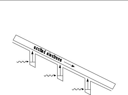
Infrared Detectors (EE)
This can be made similarly to the way the laser is made, except one deals with excitations to the conduction band and subsequent collection by the electric field. See Fig. 12.13 where the idea is sketched. One assumes the excitation energy is in the infrared.
ω
ω
ω
Fig. 12.13. Infrared photodetector made with quantum wells. As shown, the electrons in the wells are excited into the conduction band states and then can be collected and detected. Adapted from Capasso and Datta [12.8, p. 81]
12.7 Classical and Quantum Hall Effect (A)
12.7.1 Classical Hall Effect – CHE (A)
The Hall effect has been important for many reasons. For example, in semiconductors it can be used for determining the sign and the concentration of charge carriers. The fractional quantum Hall effect, in terms of basic physics ideas, may be the most important discovery in solid-state physics in the last quarter of a century. To start, we first reconsider the classical quantum Hall effect for electrons only.
Let electrons move in the (x,y)-plane with a magnetic field in the z direction and an electric field also in the (x,y)-plane. In MKS units and standard notation (e > 0)
F |
= −eE |
x |
− eV |
y |
B − |
mVx |
, |
(12.14) |
|
x |
|
|
|
τ |
|
|
|
|
|
|
|
|
|
|
|
|
Fy |
= −eEy + eVx B − |
mVy |
|
, |
(12.15) |
τ |
|
|
|
|
|
|
|
|
|
|
628 12 Current Topics in Solid Condensed–Matter Physics
where the term involving the relaxation time τ is due to scattering. The current density is given by
J x = −neVx , |
(12.16) |
J y = −neVy , |
(12.17) |
where n is the number of electrons per unit volume. Letting the dc conductivity be
σ0 = ne2τ , m
we can write (in the steady state when Fx, Fy = 0 using (12.14)–(12.18))
E |
x |
|
|
1 |
1 |
ω τ J |
x |
|
|
|
|
= |
|
|
c |
|
|
, |
|
|
|
|
|
|
Ey |
|
|
σ |
0 |
|
−ω τ |
1 |
J y |
|
|
|
|
|
|
|
|
c |
|
|
|
|
|
where ωc = eB/m is the cyclotron frequency and we can show (by (12.18))
|
|
|
|
|
|
B |
|
= |
ωcτ . |
|
|
|
|
(12.20) |
|
|
|
|
|
|
ne |
|
|
|
|
|
|
|
|
|
|
|
|
σ0 |
|
|
|
|
|
The inverse to (12.19) can be written |
|
|
|
|
|
|
|
|
|
J |
x |
|
|
|
σ0 |
|
|
1 |
−ω τ E |
x |
|
|
|
|
= |
|
|
|
|
|
c |
|
. |
(12.21) |
|
|
|
2 |
|
1 |
|
J |
y |
|
|
1+ (ω τ) |
ω τ |
E |
y |
|
|
|
|
|
|
|
|
c |
|
|
|
|
|
|
|
c |
|
|
|
|
|
|
|
|
We will use the geometry as shown in Fig. 12.14. We rederive the Hall coefficient. Setting Jy = 0, then
|
Ey = |
|
V × B |
|
= − |
ωcτ J x = − |
B |
J x , |
(12.22) |
|
|
|
|
|
|
|
|
|
|
|
|
|
σ0 |
|
|
|
|
|
ne |
|
|
where V = Vx = Jx/ne from (12.16). The Hall coefficient is defined as |
|
|
|
|
R |
= |
|
Ey |
= − |
1 |
|
|
|
|
(12.23) |
|
|
|
|
|
|
|
|
|
|
|
|
|
H |
|
|
J x Bz |
|
|
ne |
|
|
|
|
|
|
|
|
|
|
|
|
|
|
|
|
|
as usual. The Hall voltage over the length w would then be |
|
|
|
|
VH = −Ey w = |
|
BJ xw |
. |
|
|
(12.24) |
|
|
|
|
|
ne |
|
|
|
|
|
|
|
|
|
|
|
|
|
|
|
|
|
|
|
|
The current through the segment of area tw is |
|
|
|
|
|
|
|
|
|
|
|
|
|
I x = J xtw , |
|
|
|
(12.25) |
|
so |
|
|
|
|
|
|
|
|
|
|
|
|
|
|
|
|
|
|
|
|
V |
|
= |
BI x |
. |
|
|
|
(12.26) |
|
|
|
|
|
|
|
|
|
|
|
|
|
|
H |
|
|
nte |
|
|
|
|
|
|
|
|
|
|
|
|
|
|
|
|
|
|
|
|
|
|
|
|
|