10.6 Critical Points and Joint Density of States (A) |
559 |
|
|
Also,
i |
|
|
|
[H , e r] = − |
|
e p , |
(10.86) |
m |
therefore |
|
|
|
i e p j = imωij |
i e r j . |
(10.87) |
Thus we can write the oscillator strength as, |
|
|
|
i e p |
j |
2 |
|
fij = b |
|
, |
(10.88) |
m2ωij |
|
|
which is consistent with how we wrote it before, if b = −2m/ (see (10.69), (10.66)). It is also interesting to show that the oscillator strength obeys a sum rule. If e = i, then
∑ j fij = b∑ j ωij i e r j 2 |
|
|
|
= b |
∑ |
|
1 { i e p j |
j e r i − i e r j j e p i } (10.89) |
2 |
|
j im |
|
|
|
= b 1 |
|
[ i e p, e r i |
]= |
b |
[− i ]=1. |
|
2im |
2 |
im |
|
|
|
Classically, for bound states with no damping, we can derive the dielectric constant. Assume N states with frequency ω0. The result is
|
ε |
=1 |
+ |
Ne2 |
|
1 |
, |
(10.90) |
|
ε0 |
mε0 ω02 |
−ω2 |
|
|
|
|
|
which follows from (9.6) with τ → ∞ and ω0 used for several bound states labeled with i. Note that it is just the same as the quantum result (10.70) provided the oscillator strength from one oscillator is one. From this we have the index of refraction, and it is given by n2 = ε/ε0, since ε is real with τ → ∞. When ε/ε0 as the preceding, the resulting equation is often called Sellmeier’s equation.
10.6 Critical Points and Joint Density of States (A)
Optical absorption spectra give many details about the band structure. This can be explained by the Van Hove singularities, which appear in the joint density of states as mentioned below. In the integral for the imaginary part of the dielectric constant, we had an expression of the form (10.67):
εi |
2 |
∫ |
d3k |
|
Mvc |
|
2 |
δ (Ec − Ev ) . |
(10.91) |
|
|
ω2 |
(2π)3 |
|
|
|
|
|
|
|
|
|
|
|
560 10 Optical Properties of Solids
A property of delta functions can be written as
∫b g(x)δ[ f (x)]dx = ∑x |
|
g(xp ) |
1 |
, |
(10.92) |
p |
∂f |
|
|
a |
|
|
|
|
|
|
|
|
∂x |
|
x=x p |
|
|
|
|
|
|
|
|
where xp are the zeros of f(x). From which we conclude that the imaginary part of the dielectric constant can be written as
εi |
2 1 |
∫ |
|
dS |
|
M vc |
|
2 |
|
, |
(10.93) |
|
|
|
|
|
|
|
|
|
|
|
|
|
|
|
|
|
|
|
|
ω2 (2π)3 |
|
k (Ec − Ev ) |
|
|
|
|
|
s |
Ec |
−Ev = ω |
|
|
|
|
|
|
|
|
|
|
|
where dS is a surface of constant ω = Ec − Ev. The joint density of states is defined as (Yu and Cardona [10.27 p251])
Jvc = ∫ |
2 |
|
|
dS |
|
|
, |
(10.94) |
(2π)3 |
k (Ec − Ev ) |
Ec −Ev = |
|
|
ω |
|
|
|
|
|
|
|
and typically the matrix element Mvc is a slowly varying function compared with the joint density of states. Now the joint density of states is a strongly varying function of k where the denominator is zero, i.e. where
k (Ec − Ev ) = 0 . |
(10.95) |
Both valence and conduction band energies must be periodic functions in reciprocal space and so must their difference and from this it follows that there must be a point for which the denominator vanishes (smooth periodic functions have analytic maxima and minima). These critical points lead to singularities in the density of states, the Van Hove singularities. At very highly symmetrical points in the Brillouin zone, we can have critical points due to the gradient of both conduction and valence energies vanishing, at other critical points only the gradient of the difference vanishes. Critical points are defined by the band structure, and in turn, they help determine the absorption coefficient. Reversing the process, studying the absorption coefficient gives information on the band structure.
10.7 Exciton Absorption (A)
In semiconductors, one may detect absorption for energies just below the energy gap where one might have initially expected transparency. This could be due to absorption by bound electron–hole pairs or excitons. The binding energy of the excitons lowers their absorption below the bandgap energy. It is interesting that one can only think of bound electron–hole pairs if electron and holes move with the same group velocity, in other words the energy gradients of valence and electronic energies need to be the same. That is, excitons form at the critical points of the joint density of states.
10.8 Imperfections (B, MS, MET) 561
One generally talks of two kinds of excitons, the Frenkel excitons and Wannier excitons. The Frenkel excitons are tightly bound and can be described by a variant of tight binding theory. Another way to view Frenkel excitons is as a propagating excited state of a single atom. Thus, we describe it with the Hamiltonian where the states are the localized excited states of each atom. For the Frenkel case let
H = ∑i ε i i + ∑i, j Vij i j , |
(10.96) |
where with one-dimensional nearest-neighbor hopping
V |
=Vδ j +1 |
+Vδ j −1 . |
(10.97) |
ij |
i |
i |
|
This can be diagonalized by the substitution:
k = ∑ j exp(ijka) j , |
(10.98) |
which leads to the energy eigenvalues
where, εk = ε + 2V cos(ka). These Frenkel types of excitons are found in the alkali halides.
In semiconductors, the important types of excitons are the Wannier excitons, which have size much larger than typical interatomic dimensions. The Wannier excitons can be analyzed much as a hydrogen atom with reduced mass defined by the electron and hole masses and with the binding Coulomb potential reduced by the appropriate dielectric constant. That is, the energy eigenvalues are
En = Eg − |
|
|
|
μe4 |
|
|
, n =1, 2, …, |
(10.100) |
|
2 |
(4πε)2 n2 |
2 |
|
|
|
where |
|
|
|
|
|
|
|
|
|
|
|
1 |
|
= |
1 |
+ |
1 |
. |
(10.101) |
|
|
μ |
m |
|
|
|
|
|
m |
h |
|
|
|
|
|
|
e |
|
|
|
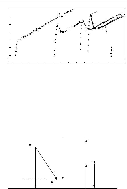
Optical absorption in GaAs is shown in Fig. 10.8.
10.8 Imperfections (B, MS, MET)
We will only give a brief discussion here. Reference should be made also to the chapters on semiconductors and defects. Imperfections may produce resonant energy levels in the bands or energy levels that are in the bandgap. Donors and acceptors in semiconductors produce energy levels that may be detected by optical absorption when the thermal energy is much less than their ionization energy. Similarly, deep defects produced in a variety of ways may produce energy levels in the gap, often near the center. Deep defects tend to be very localized in space and therefore to contain a large range of k vectors. Thus, it is possible to have
562 10 Optical Properties of Solids
|
1.2 x10⁴ |
|
|
|
|
|
|
|
|
|
|
Exciton absorption |
|
|
|
|
|
|
|
|
|
|
|
|
|
|
|
1.1 |
|
|
|
|
|
|
|
|
|
|
|
|
|
|
|
1.0 |
|
|
|
|
|
|
|
|
|
|
|
|
|
|
) |
|
|
|
|
|
|
|
|
|
|
|
|
|
|
|
–1 |
0.9 |
|
|
|
|
|
|
|
|
|
|
|
|
|
|
α(cm |
|
|
|
|
|
|
|
|
|
Absorption with formation |
|
|
|
|
|
|
|
|
|
|
0.8 |
|
|
|
|
|
|
|
|
|
of free electron hole pairs |
|
|
|
|
|
|
|
|
|
|
|
|
|
|
|
|
0.7 |
|
|
|
|
|
|
|
|
|
|
|
|
294°K |
|
|
|
|
|
|
|
|
|
|
|
|
|
|
186°K |
|
|
|
|
|
|
|
|
|
|
|
|
|
|
|
|
|
0.6 |
|
|
|
|
|
|
|
|
|
|
|
|
90°K |
|
|
|
|
|
|
|
|
|
|
|
|
|
|
21°K |
|
|
0 |
1.43 |
1.44 |
1.45 |
1.46 |
1.47 |
1.48 |
1.49 |
1.50 |
1.51 |
1.52 |
1.53 |
1.54 |
1.55 |
1.56 |
|
1.42 |
photon energy in eV
Fig. 10.8. Absorption coefficient near the band edge of GaAs. Note the exciton absorption level below the bandgap Eg [Reprinted with permission from Sturge MD, Phys Rev 127, 771 (1962). Copyright 1962 by the American Physical Society.]
a direct transition from a deep defect to a large range of k values in the conduction band, for example. A shallow level, on the other hand, is well spread out in space and therefore restricted in k value and so direct transitions from it to a band go to quite a restricted range of values. Color centers in alkali halides are examples of other kinds of optically important defects.
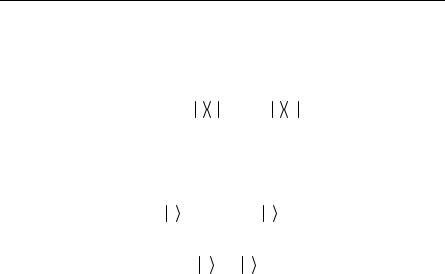
Suppose we have some generic defect with energy level in the gap. One could have absorption due to transitions from the valence or conduction band to the level. There could even be absorption between levels due to the defect or different defects. Several types of optical processes are suggested in Fig. 10.9.
Conduction Band
Donor |
|
|
Absorption |
|
Emission |
|
|
|
|
|
|
Level |
|
|
|
|
|
|
|
|
|
|
|
|
|
|
|
|
|
Deep |
|
|
|
|
|
|
|
|
|
|
|
|
|
|
Defect |
Acceptor
Level
Valence Band
Fig. 10.9. Some typical radiative transitions in semiconductors. Nonradiative (Auger) transitions are also possible

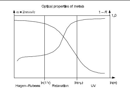
10.9 Optical Properties of Metals (B, EE, MS) 563
10.9 Optical Properties of Metals (B, EE, MS)
Free-carrier absorption can be viewed as intraband absorption–the electron absorbing the photon remains in the same band.3 Free-carrier absorption is obviously important for metals, and is often of importance for semiconductors. The electron is accelerated by the photon and gains energy, but since the wave vector of the photon is negligible, something else such as a phonon needs to be involved. For many purposes, the process can be viewed classically by Drude theory with a relaxation time of τ ≡ 1/ω0. This relaxation time defines a frictional force constant m*/τ, where the viscous like frictional force is proportional to the velocity.
We will use classical theory here, but it is worthwhile to make a few comments. It is common to deal with a semiclassical picture of radiation. There we treat the radiation classically, but the underlying electronic systems that absorb and emit the radiation we treat quantum mechanically. Radiation can be treated classically when it is intense enough to have many photons in each mode. Freeelectronic systems can be treated classically when their de Broglie wavelengths are small compared to the average interparticle separations.
The de Broglie wavelength can be estimated from the momentum as estimated from equipartition. In practice, this means that for temperatures that are not too low and densities that are not too high, then classical mechanics should be valid. Bound systems are more complicated, but in general, classical mechanics works at higher quantum numbers (higher bound-state energies). In any case, classical and quantum results often overlap in validity well beyond where one might naively expect.
The classical theory can be written, assuming a sinusoidal electric field E = E0exp(−iωt) (note these are for free-electrons (e > 0) with damping). We also generalize by using an effective mass m* rather than m:
m x + |
m |
x = −eE exp(−iωτ ) . |
(10.102) |
|
|
τ |
0 |
|
|
|
|
Note this is just (9.1) with ω0 = 0, as appropriate for free charges. Seeking a steady-state solution of the form x = x0exp(−iωτ), we find
x = |
−ieEτ |
, |
(10.103) |
|
− iωτ ) |
|
m ω(1 |
|
|
which is (9.2) with ω0 = 0. Thus, the polarization is given by |
|
P = −Nex = (ε −εL )E , |
(10.104) |
where εL is the contribution to the dielectric constant of everything except the free carriers (generalizing (9.3)). The frequency-dependent dielectric constant is
|
ε(ω) = εL + i |
Ne2τ |
|
1 |
, |
(10.105) |
|
m ω 1−iωτ |
|
|
|
|
3 See also, e.g., Ziman [25, Chap. 8] and Born and Wolf [10.1].
564 10 Optical Properties of Solids
where N is the number of electrons per unit volume. From the real and imaginary parts of ε we find, similar to Sect. 9.2,
ε |
|
= n2 − n2 = |
εL − |
|
σ0τ / ε0 |
|
, |
|
|
|
|
σ |
|
= Ne2τ |
, |
(10.106) |
|
|
|
|
|
|
|
|
|
|
|
|
|
|
|
|
r |
i |
ε0 1+ω2τ 2 |
|
|
|
|
|
|
|
0 |
m |
|
|
and |
|
|
|
|
|
|
|
|
|
|
|
|
|
|
|
|
|
|
|
|
|
|
|
|
|
|
|
|
|
|
|
|
|
|
σ |
0 |
|
1 |
|
|
|
|
|
|
|
|
|
εi = 2nni |
= |
|
|
|
|
|
|
|
|
|
|
|
|
|
|
|
. |
|
(10.107) |
|
|
ε0ω |
|
|
|
|
|
|
|
|
|
|
|
|
|
|
|
|
1+ω2τ |
2 |
|
|
|
|
It is convenient to write this in terms of the plasma frequency |
|
|
|
|
ω2p = |
Ne2 |
|
|
|
|
|
σ |
0 |
|
σ ω |
|
|
|
|
|
|
|
mε0 |
= |
|
|
|
≡ |
|
|
0 |
|
|
0 , |
|
|
(10.108) |
|
|
|
|
|
|
|
|
|
|
|
|
|
|
|
|
|
|
τε0 |
|
|
ε0 |
|
|
|
|
|
and so, |
|
|
|
|
|
|
|
|
|
|
|
|
|
|
|
|
|
|
|
|
|
|
|
|
|
|
|
|
εr |
= |
εL |
|
|
− |
|
|
ω2p |
|
|
|
|
|
, |
|
|
|
|
(10.109) |
|
|
ε0 |
|
|
|
ω02 +ω2 |
|
|
|
|
|
|
|
|
|
|
|
|
|
|
|
|
|
|
|
|
and |
|
|
|
|
|
|
|
|
|
|
|
|
|
|
|
|
|
|
|
|
|
|
|
|
|
|
|
|
εi = |
|
ω0 |
|
|
|
|
ωp2 |
|
|
|
. |
|
|
|
|
|
(10.110) |
|
|
|
ω ω02 + ω2 |
|
|
|
|
|
|
|
|
|
|
|
|
|
|
|
|
|
|
|
|
From here onwards for simplicity we assume εL ε0. We have three important ω. The plasma frequency ωp is proportional to the free-carrier concentration, ω0 measures the electron–phonon coupling and ω is the frequency of light.
We now want to show what these equations predict in three different frequency regions.
(i) ωτ << 1, the low-frequency region. We obtain by (10.109) with ω0 = 1/τ
n2 − n2 |
=1−ω2τ 2 |
, |
|
(10.111) |
|
i |
|
|
p |
|
|
|
which is small, and by (10.110) |
|
|
|
|
|
|
|
2nn |
=ω2 |
τ |
= |
(ωpτ)2 |
, |
(10.112) |
|
ωτ |
|
i |
p ω |
|
|
|
|
which is large. Here the imaginary part (of the dielectric constant) is much greater than the real part and we have high reflectivity. In this approximation
n2 − n2 |
=1−ωτ(2nn ) 1, |
(10.113) |
i |
i |
|
but neither n nor ni are small, so n ni, and n2 σ0/2ωε0. The reflectivity then becomes
R = |
(n −1) |
2 + n2 |
1− |
2 |
1 |
− 2 |
2ωε |
0 . |
(10.114) |
(n +1) |
i |
n |
σ0 |
|
2 + n2 |
|
|
|
|
|
|
|
i |
|
|
|
|
|
|
|
10.9 Optical Properties of Metals (B, EE, MS) 565
This is the Hagen–Rubens relation [10.17].
(ii) 1/τ << ω << ωp, the relaxation region. The basic relations become
n2 − n2 |
=1− |
ω2p |
, |
|
(10.115) |
|
|
|
|
i |
|
|
|
ω2 |
|
|
|
|
|
|
|
|
|
which is large and negative, and |
|
|
|
|
|
|
|
|
|
|
|
|
ωp |
2 1 |
|
|
|
|
2nn = |
|
|
|
|
|
|
|
, |
(10.116) |
|
|
|
|
|
|
i |
|
ω |
|
|
ωτ |
|
|
|
|
|
|
|
which is smaller than n2 − ni2. However, this predicts the metal is still strongly reflecting as we now show. Since ωτ >> 1 and ωp/ω >> 1, we see
|
|
|
|
ω |
p |
|
2 |
(n − n )(n + n ) − |
|
|
|
<<1, |
|
|
|
i |
i |
|
|
ω |
|
|
|
|
|
|
|
|
|
|
|
|
or |
|
|
|
|
|
|
|
|
|
|
|
|
|
ω |
p |
2 |
(n − n)(n + n ) = |
|
|
|
>>1 . |
|
ω |
|
i |
|
i |
|
|
|
|
|
|
|
|
|
|
|
|
|
Therefore,
ni >> n ,
|
|
|
|
|
|
|
|
n2 |
|
|
ω |
p |
|
2 |
|
|
|
|
|
|
|
|
|
|
|
|
|
|
|
|
|
|
|
|
|
|
|
|
, |
|
|
|
|
|
|
|
|
|
|
|
|
|
|
|
|
|
|
ω |
|
|
|
|
|
|
|
|
|
|
|
|
|
|
|
|
|
|
|
|
i |
|
|
|
|
|
|
|
|
|
|
|
|
|
|
|
|
|
|
|
|
|
|
|
|
|
|
|
|
|
|
|
|
|
|
|
|
|
|
|
|
|
|
|
|
|
|
|
|
|
|
|
|
|
|
|
|
n |
|
|
|
ωp |
|
, |
|
|
|
|
|
|
|
|
|
|
|
|
|
|
|
|
|
|
|
|
|
ω |
|
|
|
|
|
|
|
|
|
|
|
|
|
|
|
|
|
|
|
|
|
i |
|
|
|
|
|
|
|
|
|
|
|
|
|
|
|
|
|
|
|
|
|
|
|
|
|
2nn |
|
n2 |
|
|
1 |
|
, |
|
|
|
|
|
|
|
|
|
|
|
|
|
|
|
|
|
|
|
ωτ |
|
|
|
|
|
|
|
|
|
|
|
|
|
|
|
|
|
i |
|
|
|
i |
|
|
|
|
|
|
|
|
|
|
|
|
|
(n −1) |
2 + n |
2 |
|
1+[(n −1) / n |
]2 |
|
|
|
n −1 |
2 |
n +1 |
2 |
|
R = |
|
|
i |
= |
|
|
|
|
|
|
|
|
i |
|
|
|
|
|
|
|
|
|
|
|
|
|
, |
(n +1) |
2 |
+ n |
2 |
1 |
+[(n +1) / n |
] |
2 |
|
1+ |
n |
|
− |
n |
|
|
|
|
|
|
|
|
|
|
|
i |
|
|
i |
|
|
|
|
|
i |
|
|
|
|
|
|
|
|
|
i |
|
|
|
|
|
|
|
|
|
|
|
|
|
|
and |
|
|
|
|
|
|
|
|
|
|
|
|
|
|
|
|
|
|
|
|
|
|
|
|
|
|
|
|
|
|
|
|
|
|
|
|
|
R =1− |
4n |
|
|
=1− |
|
2 |
. |
|
|
|
|
|
|
|
|
|
|
|
|
|
|
|
|
|
ωpτ |
|
|
|
|
|
|
|
|
|
|
|
|
|
|
|
|
|
n2 |
|
|
|
|
|
|
|
|
|
|
|
|
|
|
|
|
|
|
|
|
|
|
|
|
|
|
|
i |
|
|
|
|
|
|
|
|
|
|
|
|
|
|
|
|
|
|
|
(10.119)
(10.120)
(10.121)
(10.122)
(10.123)
(10.124)
Since ωpτ >> 1, the metal is still strongly reflecting.
566 10 Optical Properties of Solids
Fig. 10.10. Sketch of absorption and reflection in metals
(iii)ωp << ω or ωp/ω << 1. This is the ultraviolet region where we also assume
ω>> ω0.
(n2 − n2 ) 1 , |
(10.125) |
i |
|
so |
|
(n − ni )(n + ni ) =1 . |
(10.126) |
2nni = (ωp/ω)2(1/ωτ) is very small. Both n and ni are not very small, therefore ni is very small. Therefore,
|
|
n >> ni , n 1. |
|
|
|
(10.127) |
Therefore, |
|
|
|
|
|
|
|
|
|
|
|
|
|
|
|
|
|
|
|
1 |
|
ωp 2 |
1 |
|
|
|
|
|
n |
|
|
|
|
|
|
|
|
|
|
. |
|
(10.128) |
|
2 |
ω |
|
|
ωτ |
|
|
i |
|
|
|
|
|
|
|
|
|
|
|
|
|
|
|
|
|
|
|
|
|
|
|
|
|
So, |
|
|
|
|
|
|
|
|
|
|
|
|
|
|
|
|
|
n2 |
|
n |
2 |
|
|
|
|
1 |
|
ωp 4 |
1 |
|
R |
i |
|
i |
|
|
|
|
|
|
|
|
|
|
|
(10.129) |
|
|
|
|
|
|
|
|
(ωτ)2 |
ni2 + 4 |
|
4 |
|
|
16 |
|
ω |
|
|
|
is very small. There is little reflectance since this is the ultraviolet transparency region. We summarize our results in Fig. 10.10. See also Seitz [82, p 639], Ziman [25, 1st edn, p 240], and Fox [10.12].
10.9 Optical Properties of Metals (B, EE, MS) 567
The plasma edge, or the region around the plasma frequency deserves a little more attention. Using Maxwell’s equations we have
|
× E = − |
∂B |
, |
|
E = B = 0 (ρ = 0) , |
(10.130) |
|
|
|
|
|
∂t |
|
|
|
|
|
|
and |
|
|
|
|
|
|
× B = |
μ0 |
∂ 2D |
( j = 0) , |
(10.131) |
|
∂ t2 |
|
|
|
|
|
|
|
|
|
and we will include any charge motion in P. Therefore, |
|
|
2E = μ |
|
∂ 2D , |
D = ε εE . |
(10.132) |
|
|
|
|
0 |
∂ t2 |
0 |
|
Note here ε→ε/ε0. Assume E = E0exp(−iωt)exp(ik r). We obtain, as shown below ((10.142), (10.143)), for the wave vector
k |
2 |
= ε(ω)μ0ε0ω |
2 |
2 |
2 |
~2 |
(10.133) |
|
|
(kc) = ε(∞)(ω |
|
−ωp ) . |
For a free-electron in an electric field we have already derived the plasma frequency in Sect. 9.4. We give here an alternative simple derivation and bring out a few new features,
|
|
m |
d2 x |
= −eE , |
|
|
|
|
|
dt2 |
|
|
|
|
|
|
|
|
|
|
|
|
|
|
|
|
x = x0 exp(−iωt) , |
|
|
E = E0 exp(−iωt) , |
|
|
|
|
|
x = |
|
eE |
|
|
. |
|
|
|
|
|
|
|
mω2 |
|
|
|
|
|
|
|
|
|
|
|
|
|
Also, |
|
|
|
|
|
|
|
|
|
|
|
|
|
P = −Nex = − |
Ne2 |
|
E , |
|
|
mω2 |
|
|
|
|
|
|
|
|
|
|
|
|
|
|
ε(ω) =1 |
+ |
|
P(ω) |
|
=1− |
|
Ne2 |
, |
|
ε0E(ω) |
ε0mω2 |
|
|
|
|
|
|
|
|
|
|
ω2p = |
Ne2 |
, |
|
|
|
|
|
|
|
|
|
ε0m |
|
|
|
|
ω2 ε(ω) =1 − ω2p .
(10.134)
(10.135)
(10.136)
(10.137)
(10.138)
(10.139)
(10.140)
(10.141)
568 10 Optical Properties of Solids
If the positive ion core background has a dielectric constant of ε(∞) that is about constant, then (10.141) is modified
|
|
|
|
~ |
2 |
|
|
ε(ω) = ε(∞) |
|
− |
ωp |
, |
(10.142) |
1 |
ω |
2 |
|
|
|
|
|
|
|
|
|
where |
|
|
|
|
|
|
|
~ |
ω p |
. |
|
|
(10.143) |
ω p = |
|
|
|
|
|
|
ε(∞) |
|
|
|
When the frequency is less than the plasma frequency the squared wave vector is negative (10.133) and gives us total reflection. Above the plasma frequency, the wave vector squared is positive and the material is transparent. That is, simple metals should reflect in the visible and be transparent in the ultraviolet, as we have already seen.
It is also good to remember that at the plasma frequency the electrons undergo low-frequency longitudinal oscillations. See Sect. 9.4. Specifically, note that setting ε(ω) = 0 defines a frequency ω = ωL corresponding to longitudinal plasma oscillations.
|
ε(ω) =1 − |
ω2p |
, so ε(ω) = 0 implies ω = ωp . |
(10.144) |
|
ω2 |
|
|
|
|
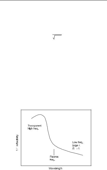
Here we have neglected the dielectric constant of the positive ion cores.
The plasma frequency is also a free longitudinal oscillation. If we have a doped semiconductor with the plasma frequency less than the bandgap over Planck’s constant, one can detect the plasma edge, as illustrated in Fig. 10.11. See also Fox op cit, p156. Hence, we can determine the electron concentration.
Fig. 10.11. Reflectivity of doped semiconductor, sketch