

Finkenzeller K.RFID handbook.2003
.pdf11.4 CONNECTION OF ANTENNAS FOR INDUCTIVE SYSTEMS |
323 |
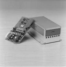
Figure 11.19 Reader with integral antenna and matching circuit (MIFARE -reader, reproduced by permission of Philips Electronics N.V.)
by a suitable layout (stripline). The matching circuit is clearly visible on the inside of the antenna coil (SMD component).
Before we can dimension the circuit, we first need to determine the impedance ZA of the antenna coil for the operating frequency by measurement. It is clear that the impedance of a real antenna coil is generated by the serial connection of the coil inductance LS with the ohmic wire resistance RLS of the wire. The serial connection from XLS and RLS can also be represented in the impedance level.
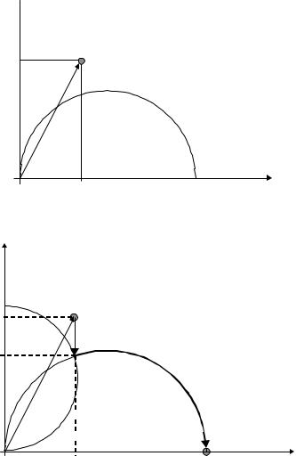
The function of the matching circuit is the transformation of the complex coil impedance ZA to a value of 50 real. A reactance (capacitance, inductance) in series with the coil impedance ZA shifts the total impedance Z in the direction of the j X axis, while a parallel reactance shifts the total impedance away from the origin in a circular path (Figure 11.20).
The values of C2p and C2s are dimensioned such that the resulting coil impedance ZA is transformed to the values desired to achieve 50 .
The matching circuit from Figure 11.18 can be mathematically represented by
equation 11.4: |
|
|
|
|
|
|
|
|
|
|
|
|
Z0 = 50 = |
|
|
|
|
|
1 |
|
|
|
|
|
(11.4) |
|
|
|
|
|
|
|
|
|
|
|
||
− |
j ωC2p |
|
|
|
|
|
1 |
|
|
|
||
|
|
|
1 |
|
|
|
|
|
||||
|
|
+ |
|
|
+ |
RLs |
+ |
j ωLs |
|
|
||
|
|
|
|
|
j ωC1s |
|
||||||
|
|
|
|
|
− |
|
|
|
|
|||
|
|
|
|
|
|
|
|
|
|
|
|
From the relationship between resistance and conductance in the complex impedance plane (Z-level), we find the following relationship for C2p:
|
= |
ωZ0RLS |
|
C2p |
|
Z0 · RLs − RLs2 |
(11.5) |
324 |
11 READERS |
jX 
ZA
XLs
RLs |
Z0 (50 Ω) |
R |
Figure 11.20 Representation of ZA in the impedance level (Z plane)
jX |
|
XC2p |
ZA |
XLs |
|
|
C1 1/(XLs - XC2s) |
XC2s |
|
C2 ~ 1/XC2p
RLs |
|
Z0 (50 Ω) |
R |
|
|||
|
Figure 11.21 Transformation path with Cls and C2p
As is clear from the impedance plane in Figure 11.21, C2p is determined exclusively by the serial resistance Rls of the antenna coil. For a serial resistance RLS of precisely 50 , C2p can be dispensed with altogether; however greater values for Rls are not permissible, otherwise a different matching circuit should be selected (Fricke et al., 1979).
We further find for Cls:
C1s = |
|
|
|
|
1 |
|
|
(11.6) |
|
Ls |
|
|
|
|
|
||
ω2 |
|
|
Z0RLS − RLS2 |
|
||||
|
|
|
|
|
||||
|
− |
|
ω |
|
||||
|
|
· |
|
|
||||
|
|
|
|
|
|
|
|
|
11.5 READER DESIGNS |
327 |
||
|
Table 11.2 Typical technical data |
||
|
|
|
|
|
Supply voltage: |
Typically 12 V |
|
|
Antenna: |
External |
|
|
Antenna connection: |
BNC box, terminal screw or soldered connection |
|
|
Communication interface: |
RS232, RS485 |
|
|
Communication protocol: |
X-ON/X-OFF, 3964, ASCII |
|
|
Environmental temperature: |
0–50 ◦ C |
|
Table 11.3 Typical technical data
|
Supply voltage: |
|
Typically 24 V |
|
|
Antenna: |
|
External |
|
|
Antenna terminal: |
|
BNC socket or terminal screw |
|
|
Communication interface: |
RS485, RS422 |
||
|
Communication protocol: |
3964, InterBus-S, Profibus, etc. |
||
|
Ambient temperature: |
|
−25–+80 ◦C |
|
|
Protection types, tests: |
IP 54, IP 67, VDE |
||
|
|
|
||
|
Table 11.4 Typical technical data |
|||
|
|
|||
Supply voltage: |
Typically 6 V or 9 V from batteries or accumulators |
|||
Antenna: |
Internal, or as “sensor” |
|||
Antenna terminal: |
|
— |
||
Communication interface: |
Optional RS232 |
|||
Ambient temperature: |
0–50 ◦C |
|
|
|
Protection types, tests: |
IP 54 |
|
|
|
Input/output elements |
LCD display, keypad |
|||
|
|
|
|
|
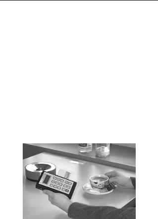
Figure 11.24 Reader for portable use in payment transactions or for service purposes. (Photo of LEGIC reader reproduced by permission of Kaba Security Locking Systems AG, CH-Wetzikon)
11.5.2 Readers for industrial use
Industrial readers are available for use in assembly and manufacturing plant. These usually have a standardised field bus interface for simple integration into existing systems. In addition, these readers fulfil various protection types and explosion protected readers (EX) are also available.
328 |
11 READERS |
11.5.3 Portable readers
Portable readers are used for the identification of animals, as a control device in public transport, as a terminal for payments, as an aid in servicing and testing and in the commissioning of systems. Portable readers have an LCD display and a keypad for operation or entering data. An optional RS232-interface is usually provided for data exchange between the portable readers and a PC.
In addition to the extremely simple devices for system evaluation in the laboratory, particularly robust and splash-proof devices (IP 54) are available for use in harsh industrial environments.
RFID Handbook: Fundamentals and Applications in Contactless Smart Cards and Identification, Second Edition
Klaus Finkenzeller Copyright 2003 John Wiley & Sons, Ltd.
ISBN: 0-470-84402-7
12
The Manufacture
of Transponders and
Contactless Smart Cards
12.1Glass and Plastic Transponders
A transponder is made up of two components: the electronic data carrier and the housing. Figure 12.1 gives a simplified representation of the manufacturing process for an inductively coupled transponder.
12.1.1 Module manufacture
In accordance with the normal semiconductor manufacturing procedure, the microchip is produced on a so-called wafer. This is a slice of silicon, which may be 6 inches in diameter, upon which several hundred microchips are produced simultaneously by repeated doping, exposure, etching and washing of the surface.
In the next stage of production, the microchips on the wafer are contacted using metal points and then each of the chips is individually tested for functionality. The chips have additional contact fields for this purpose, which give direct access — i.e. without going through the HF interface — to the chip’s memory and security electronics. The chips are placed in so-called test mode during this procedure, which permits unlimited direct access to all functional groups upon the chip. The functional test can therefore be performed significantly more intensively and comprehensively than would be possible later on, when communication can only taken place via the contactless technology.
All defective chips are marked with a red ink dot at this stage, so that they can be identified and separated out in the subsequent stages of production. The test mode can also be used to programme a unique serial number into the chip, if the chip has an EEPROM. In read-only transponders, the serial number is programmed by cutting through predefined connecting lines on the chip using a laser beam.
After the successful completion of the test programme the test mode is deactivated by permanently breaking certain connections (so-called fuses) on the chip by a strong
12.1 GLASS AND PLASTIC TRANSPONDERS |
331 |
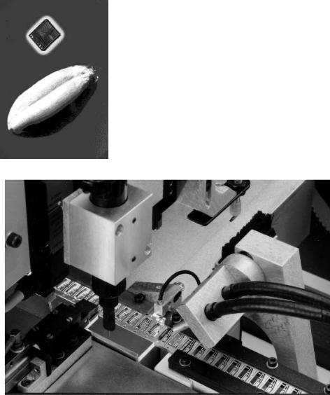
Figure 12.2 Size comparison of a sawn die with a cereal grain. The size of a transponder chip varies between 1 mm2 and 15 mm2 depending upon its function (photo: HITAG Multimode-Chip, reproduced by permission of Philips Electronics N.V.)
Figure 12.3 Manufacture of plastic transponders. In the figure an endless belt is fitted with transponder coils wound onto a ferrite core. After the transponder chip has been fitted and contacted, the transponder on the belt is sprayed with plastic (reproduced by permission of AmaTech GmbH & Co. KG, Pfronten)
to the normal insulating paint. The winding tool is heated to the melting point of the baked enamel during the winding operation. The enamel melts during winding and hardens rapidly when the coil has been removed from the winding tool, causing the individual windings of the transponder coil to stick together. This guarantees the mechanical stability of the transponder coil during the following stages of assembly. See Figure 12.3.

332 12 THE MANUFACTURE OF TRANSPONDERS AND CONTACTLESS SMART CARDS
Immediately after the winding of the transponder coil, the coil connections are welded to the contact surface of the transponder module using a spot welding machine. The shape and size of the transponder coil are determined by the format of the finished transponder.
In dice that are not immediately fitted into a module, the copper wire can be bonded directly to the die using a suitable procedure. However, this requires that the wire of the transponder coil is as thin as possible. For this reason, the transponder coil of a glass transponder is wound from wire that is only 30 µm thick.
Once the transponder coil has been contacted, the transponder is electrically functional. Therefore a contactless functional test is carried out at this stage to sort out those transponders that have been damaged during preceding stages. Transponders that have not yet been fitted into housings are called semi-finished transponders, as they can go from this stage into different housing formats.
12.1.3 Completion
In the next stage, the semi-finished transponder is inserted into a housing. This may take place by injection moulding (e.g. in ABS), casting, pasting up, insertion in a glass cylinder, or other procedures.
After a further functional test, the application data and/or application key can be loaded into the transponder, if required.
12.2Contactless Smart Cards
Contactless smart cards represent a very common special type of transponder. DIN/ISO 7810 specifies the format for all ID and smart cards. The dimensions of a smart card are specified as 85.46 mm × 53.92 mm × 0.76 mm (± tolerances). The required thickness of just 0.76 mm represents a particular challenge for the manufacture of contactless smart cards because this places strict limits on the possible dimensions of the transponder coil and chip module.
A contactless smart card may, for example, be manufactured from four PVC foils of around 0.2 mm thickness: two inlet foils that are inserted in the inside of the card and two overlay foils that will form the outside of the card. Contactless smart cards are produced in sheets of 21, 24 or 48. The foils used thus have an area of around 0.1 to 0.3 m2. The typical foil structure of a contactless smart card is shown in Figure 12.4. The two overlay foils are printed with the layout of the smart card. On modern printing machines a high-quality coloured print is possible, such as that familiar from telephone smart cards.
The antenna in the form of a coil is applied to one of the two inlet foils, the carrier foil, and connected to the chip module using a suitable connection technique. Four main procedures are used for the manufacture of the antenna coil: winding, embedding, screen printing and etching.
The carrier foil is covered by a second inlet foil, from which the area of the chip module has been stamped out. Often a filler is also dosed into the remaining hollow space. This filling is necessary to prevent the overlay foils applied after the lamination