Добавил:
Опубликованный материал нарушает ваши авторские права? Сообщите нам.
Вуз: Предмет: Файл:

Finkenzeller K.RFID handbook.2003

.pdf
Скачиваний:
232
Добавлен:
23.08.2013
Размер:
6.09 Mб
Скачать

282

10 THE ARCHITECTURE OF ELECTRONIC DATA CARRIERS

Figure 10.11 Size comparison: low-cost transponder chip in the eye of a needle (reproduced by permission of Philips Electronics N.V.)

sensitive applications may be impaired by unauthorised reading or writing of data in the transponder. Two examples of such applications are the contactless cards used as tickets in the public transport system and transponders in vehicle keys for electronic immobilisation systems.

There are various procedures for preventing unauthorised access to a transponder. One of the simplest mechanisms is read and write protection by checking a password. In this procedure, the card compares the transmitted password with a stored reference password and permits access to the data memory if the passwords correspond.

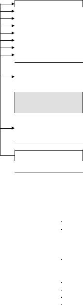
However, if mutual authorisation is to be sought or it is necessary to check that both components belong to the same application, then authentication procedures are used. Fundamentally, an authentication procedure always involves a comparison of two secret keys, which are not transmitted via the interface. (A detailed description of such procedures can be found in Chapter 8). Cryptological authentication is usually associated with the encryption of the data stream to be transmitted (Figure 10.12). This provides an effective protection against attempts to eavesdrop into the data transmission by monitoring the wireless transponder interface using a radio receiver.

In addition to the memory area allocated to application data, transponders with cryptological functions always have an additional memory area for the storage of the secret key and a configuration register (access register, Acc) for selectively write protecting selected address areas. The secret key is written to the key memory by the manufacturer before the transponder is supplied to the user. For security reasons, the key memory can never be read.

Hierarchical key concept Some systems provide the option of storing two separate keys — key A and key B — that give different access rights. The authentication between transponder and reader may take place using key A or key B. The option of

10.1 TRANSPONDER WITH MEMORY FUNCTION

283


Modulator


Coil 1


Crypto circuit


Mode register


endfrontAnalog

Write decoder


generator

Adapt

OP-code detect


Controller

Memory


crypto control

(320 bit EEPROM)


Coil 2


EEPROM control

crypto key

HV


Bitrate generator

read/write control


64 or 128 bit


ID code


Testlogic

Input register

POR


VDD VSS


Testpads


Figure 10.12 Block diagram of a writable transponder with a cryptological function to perform authentication between transponder and reader (reproduced by permission of TEMIC Semiconductor GmbH, Heilbronn)

allocating different access rights (Acc) to the two keys may therefore be exploited in order to define hierarchical security levels in an application.

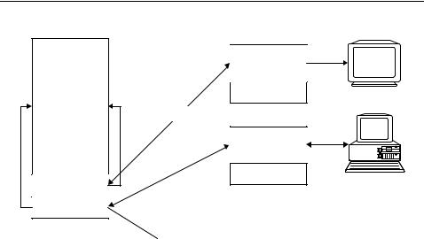
Figure 10.13 illustrates this principle for clarification. The transponder incorporates two key memories, which are initialised by the two keys A and B. The access rights that the readers are allocated after successful authentication depends upon the setting that has been selected in the transponder (access register) for the key that has been used.

Reader 1 is only in possession of key A. After successful authentication, the selected settings in the access register (Acc) only permit it to read from the transponder memory. Reader 2, on the other hand, is in possession of key B. After successful authentication using key B, the settings selected in the access register (Acc) permit it to write to the transponder memory as well as reading from it.

Sample application — hierarchical key Let us now consider the system of travel passes used by a public transport network as an example of the practical use of hierarchical keys. We can differentiate between two groups of readers: the ‘devaluers’ for fare payments and the ‘revaluers’ which revalue the contactless smart cards.

The access rights to the transponder’s two access registers A and B are configured such that, after successful authentication using key A, the system only permits the deduction of monetary amounts (the devaluation of a counter in the transponder). Only after authentication with key B may monetary amounts be added (the revaluation of the same counter).

In order to protect against attempted fraud, the readers in vehicles or subway entrances, i.e. devaluers, are only provided with key A. This means that a transponder can never be revalued using a devaluer, not even if the software of a stolen devaluer is manipulated. The transponder itself refuses to add to the internal counter unless the transaction has been authenticated by the correct key.

284


10 THE ARCHITECTURE OF ELECTRONIC DATA CARRIERS


Read only


Reader 1


Application

Key A


data


Authentication


Reader 2


Key B


Key A/Acc A

Read & write


Key B/Acc B


Transponder

Key & “access right


of the key” (Acc)

Figure 10.13 A transponder with two key memories facilitates the hierarchical allocation of access rights, in connection with the authentication keys used

The high-security key B is only loaded into selected secure readers that are protected against theft. The transponder can only be revalued using these readers.

10.1.3.4Segmented memory

Transponders can also be protected from access by readers that belong to other applications using authentication procedures, as we described in a previous chapter. In transponders with large memory capacities, it is possible to divide the entire memory into small units called segments, and protect each of these from unauthorised access with a separate key. A segmented transponder like this permits data from different applications to be stored completely separately (Figure 10.14).

Access to an individual segment can only be gained after successful authentication with the appropriate key. Therefore, a reader belonging to one application can only gain access to its ‘own’ segment if it only knows the application’s own key.

The majority of segmented memory systems use fixed segment sizes. In these systems, the storage space within a segment cannot be altered by the user. A fixed segment size has the advantage that it is very simple and cheap to realise upon the transponder’s microchip.

However, it is very rare for the storage space required by an application to correspond with the segment size of the transponder. In small applications, valuable storage space on the transponder is wasted because the segments are only partially used. Very large applications, on the other hand, need to be distributed across several segments, which means that the application specific key must be stored in each of the occupied segments. This multiple storage of an identical key also wastes valuable storage space.

A much better use of space is achieved by the use of variable length segments (Figure 10.15). In this approach, the memory allocated to a segment can be matched to

10.1 TRANSPONDER WITH MEMORY FUNCTION

285

Security encoding

P

Appl. X

Appl. Y

RFU


RFU

(planned)

(planned)


RFU

RFU

RFU

RFU

RFU

RFU

RFU

RFU

Figure 10.14 Several applications on one transponder — each protected by its own secret key

Segment 1

Key/Acc/Len 1


Key/Acc 1


Segment 1

Segment 2


Key/Acc 2


Segment 3

Key/Acc/Len 2


Key/Acc 3

Segment 2


Fixed segmentation

Free (variable) segmentation

Figure 10.15 Differentiation between fixed segmentation and free segmentation

the requirements of the application using the memory area. Because of the difficulty in realising variable segmentation, this variant is rare in transponders with state machines.

Figure 10.16 illustrates the memory configuration of a transponder with fixed segmentation. The available memory, totalling 128 bytes, is divided into four segments, known as ‘pages’. Each of the four segments can be protected against unauthorised reading or writing by its own password. The access register of this transponder (‘OTP write protection’) consists of an additional memory area of 16 bits per segment. Deleting a single bit from the access register permanently protects 16 bits of the application memory against overwriting.

286

10 THE ARCHITECTURE OF ELECTRONIC DATA CARRIERS

4 pages 16 words of 16 bit

0

1

2

3

4

5

6

7

8

9

A B

C

D

E

F

0

1

Memory map of a 1 Kbit (128 byte)

RFID memory

OTP write protection bit for each 16-bit word

16-bit write password for the chip

32-bit read/write password available for any page

Security register

32 bit chip identification number

Figure 10.16 Example of a transponder with fixed segmentation of the memory (IDESCO MICROLOG ) The four ‘pages’ can be protected against unauthorised reading or writing using different passwords (IDESCO, n.d.)

10.1.3.5 MIFARE application directory

The memory of a MIFARE transponder is divided into 16 independent segments, known as sectors. Each sector is protected against unauthorised access by two different keys (hierarchical structure). Different access rights can be allocated to each of the two keys in its own access register (config.). Thus, 16 independent applications that are protected from each other by secret keys can be loaded onto the transponder (Figure 10.17). None of the applications can be read without the secret key, not even for checking or identification. So it is not even possible to determine what applications are stored on the transponder.

Let us now assume that the city of Munich has decided to issue a contactless CityCard, which citizens can use to avail themselves of city services, and which occupies

10.1 TRANSPONDER WITH MEMORY FUNCTION

287

Sector 0

Sector 1

Sector 3

Sector 4

Sector 5

Sector 0xC

Sector 0xD

Sector 0xE

Sector 0xF


MIFARE® chip

‘Manufacturer block’


S = 0, Y = 0, mblk.


SNr

Manufacturer’s data


S = 0, Y = 1, data


Sector trailer


S = 0, Y = 2, data


Access


S = 0, Y = 3,


Key 1


config.


Key 2


trailer


(ACC)


Data blocks


S = X, Y = 0, data


Write-/read block (16 byte)


S = X, Y = 1, data


S = X, Y = 2, data


Value-block


S = X, Y = 3, trailer


16 sectors × 4 blocks × 16 bytes

Figure 10.17 Memory configuration of a MIFARE data carrier. The entire memory is divided into 16 independent sectors. Thus a maximum of separate 16 applications can be loaded onto a MIFARE card

only a small part of the available memory on the card. The remaining memory units on the card could be used by other service providers for their own applications, such as local transport tickets, car rental, filling station cards, parking passes, bonus cards for restaurants and supermarket chains, and many others. However, we cannot find out which of the many possible applications are currently available on the card, because each reader belonging to an application only has access to its own sector, for which it also has the correct key.

To get around this problem, the author, in conjunction with Philips Semiconductors Gratkorn (was Mikron), has developed an application directory for the MIFARE smart card. Figures 10.18 and 10.19 illustrate the data structure of this directory, the MAD (MIFARE application directory).

Blocks 1 and 2 of sector 0 are reserved for the MAD, leaving 32 bytes available for the application directory. Two bytes of each make up a pointer, ID1 to ID$F, to one of the remaining 15 sectors. Reading the content of the pointer yields 2 bytes, the function cluster and the application code, which can be used to look the application up in an external database. Even if the application we are looking for is not registered in the available database, we can still gain an approximate classification from the function cluster, for example ‘airlines’, ‘railway services’, ‘bus services’, ‘city card services’, ‘ski ticketing’, ‘car parking’, etc.

Each application is allocated a unique identification number, made up of the function cluster code and application code. It is possible to request an identification number from the developer of MIFARE technology, Philips Semiconductors Gratkorn (Mikron) at Graz.

If a function cluster is set at 00 h, then this is an administration code for the management of free or reserved sectors.

288

10 THE ARCHITECTURE OF ELECTRONIC DATA CARRIERS

Sector 0

Sector 1

Sector 2

Sector 3

Sector 4

Sector 5 ...

Sector 0xE

Sector 0xF

16 sectors × 4 blocks × 16


S = 0, Y = 0, manufacturer-block


S = 0, Y = 0, manuf. block


SNR


TAG, size, ...

Production


S = 0, Y = 1, directory


Y = 3, sector trailer:


S = 0, Y = 2, directory


Key A


Access

GPB

Key B


conditions


S = 0, Y = 3, trailer


0x69: Card not personalized


non-standard


Sector 0


Bit 8


Bit 0


Y = 1..2, Application directory:


INFO


ID7

ID6

ID5

ID4


ID3


ID2

ID1


R.F.U.


CRC


ID$F

ID$E

ID$D

ID$C


ID$B


ID$A

ID9

ID8


APPL (1 = multi/


DIR version


0 = mono)


Byte 0xF


Byte 0


DIR available (1 = yes/0 =


Read with write with


Increment Dec, trf, rst


key:

key:


with key:

with key:


INFO: 1 byte header, 1 byte 8-bit-CRC


A/B

B

-


-


IDn: 2 bytes application identifier, sector n


Figure 10.18 The data structure of the MIFARE application directory consists of an arrangement of 15 pointers (ID1 to ID$F), which point to the subsequent sectors


S = 0, Y = 1..2, application directory


@Y = 1

ID7

ID6

ID5

ID4

ID3


ID2

ID1


INFO


CRC


@Y = 2

ID$F

ID$E

ID$D

ID$C

ID$B


ID$A

ID9

ID8


Byte 0xF


Byte 0


Application-ID for sector-X: 2 byte:


MSB


LSB


Function cluster

Application code


Info: 2 bytes


MSB


LSB


Info-byte


8 bit-CRC


Bit 8


Bit 0


R.F.U.

Pointer to CPS

(CPS = Card publisher sector)

8 bits (256 allocations)

8 bits (256 allocations)

01h ... FFh = Function cluster

00h = Administration-code (prefix)

00h ... FFh = Application code (cluster<>00h)

00h ... FFh = Administration code (suffix)

#00 00h sector free #00 01h sector

#00 02h sector reserved

#00 03h DIR continued (future) #00 04h card holder (name, sex)

# .... r.f.u.

Figure 10.19 Data structure of the MIFARE application directory: it is possible to find out what applications are located in each sector from the contents of the 15 pointers (ID1 to ID$F)

Sector 0 itself does not require an ID pointer, because the MAD itself is stored in sector 0. The 2 bytes that this leaves free are used to store an 8-bit CRC, which is used to check the MAD structure for errors, and an info byte. A note can be recorded in the lowest 4 bits of the info byte, giving the sector ID of the card publisher. In our example, this would be the sector ID of one of the sectors in which the data belonging to the city of Munich is stored. This allows the reader to determine the card publisher, even if more than one application is recorded on the smart card.

10.1 TRANSPONDER WITH MEMORY FUNCTION

289

Another special feature is MAD’s key management system. While key A, which is required for reading the MAD, is published, key B, which is required for recording further applications, is managed by the card publisher. This means that joint use of the card by a secondary service provider is only possible after a joint use contract has been concluded and the appropriate key issued.

10.1.3.6Dual port EEPROM

EEPROM modules with a serial I 2C (IIC ) bus interface established themselves years ago, particularly in consumer electronics. I2C bus is the abbreviation for Inter IC bus, because originally it was developed for the connection of microprocessors and other ICs on a common printed circuit board. The I2C bus is a serial bus and requires only two bidirectional lines, SDA (Serial Data) and SCL (Serial Clock). A serial EEPROM can be read or written by the transmission of defined commands via the two lines of the I2C bus.

Some of these serial EEPROM modules now also have an HF interface and can thus be read or written either via the two SDA and SCL lines or via the contactless interface. The block diagram of such a dual port EEPROM (Atmel, 1998) is shown in Figure 10.20.


VCC


RFVCC


Corevcc


Power management


and control


L1


Analog


SDA


L2


interface


RF


Serial


SCL


control


control


PROT


WP


Arbitration

GND

8 K EEPROM Test 8 pages

(8 × 128 each)

Access protection

Identification #

Figure 10.20 Block diagram of a dual port EEPROM. The memory can be addressed either via the contactless HF interface or an IIC bus interface (reproduced by permission of Atmel Corporation, San Jose, USA)

290

10 THE ARCHITECTURE OF ELECTRONIC DATA CARRIERS

The EEPROM is accessed via two state machines (‘RF control’ and ‘serial control’) that are largely independent of each other. The additional arbitration logic prevents conflicts as a result of simultaneous access to the EEPROM via the HF and serial interfaces by simply blocking access to the other interface for the duration of a write or read operation.

The HF interface of the module is designed for inductive coupling in the frequency range of 125 kHz. If no supply voltage is available via the Vcc pin of the module, then the dual port EEPROM can also be supplied with power entirely via the HF interface. The integral power management simply switches off parts of the circuit that are not required in pure contactless operation. The data transfer from the serial EEPROM to a contactless reader takes place by ohmic load modulation in the baseband. Commands from a reader are transferred to the dual port EEPROM by a simple ASK modulation (modulation index m > 10%). See Figures 10.21 and 10.22 for the pin assignment and memory configuration.

The total memory space of 1 Kbyte (8 Kbit) available on the dual port EEPROM was divided into eight segments (blocks 0–7). Each of these eight blocks was subdivided into eight subsegments (pages 0–7), each of 16 bytes. An additional 16 bytes are available as an access protection page. The structure of the access protection page is shown in Figure 10.23. The access protection page permits different access rights to the eight blocks of the EEPROM to be set independently of each other for the I2C bus and the HF interface. However, read and write access to the access protection page itself is only possible via the I2C bus interface.

The access rights of the HF interface on memory block Y are defined in the bits RFY of the access protection page (e.g. RF7 contains the access rights on block 7) (Table 10.2). In a similar manner, the access rights of the I2C bus interface are defined on a memory block Y in the bit PBY of the access protection page (PB5 contains access rights on block 5).

Furthermore, block 0 permits the access rights of the individual 16 byte pages of the block to be set independently of each other. Bits WP7–WP0 of the access protection page serve this purpose.

A peculiarity is the tamper bit in the access protection page. This bit can be set only to ‘1’ by the HF interface and only to ‘0’ by the I2C bus interface. In this manner a previous write or read access of the EEPROM via the HF interface can be signalled to the master of the connected I2C bus.

L1


1

8


VCC


L2


2

7


WP


PROT


3

6


SCL


GND


4

5


SDA


Figure 10.21 Pin assignment of a dual port EEPROM. The transponder coil is contacted to pins L1 and L2. All other pins of the module are reserved for connection to the I2C bus and for the power supply in ‘contact mode’ (reproduced by permission of Atmel Corporation, San Jose, USA)

10.1 TRANSPONDER WITH MEMORY FUNCTION

291

Block 0, page 0: 16 bytes

Block 0, page 1, 16 bytes

Block 0, page 2, 16 bytes

Block 0, page 3, 16 bytes

Block 0, page 4, 16 bytes

Block 0, page 5, 16 bytes

Block 0, page 6, 16 bytes

Block 0, page 7, 16 bytes

Block 1: 128 bytes

Block 7: 128 bytes

Access register: 16 bytes

Unique chip ID: 16 bytes

Figure 10.22 Memory configuration of the AT24RF08. The available memory of 1 Kbyte is split into 16 segments (blocks 0–7) of 128 bytes each. An additional memory of 32 bytes contains the access protection page and the unique serial numbers. The access protection page permits different access rights to be set in the memory for the HF and I2C bus interface

bit 7

bit 6 bit 5 bit 4 bit 3 bit 2

bit 1

bit 0


SB0


RF0


PB0

Addr 0


Addr 1

SB1


RF1


PB1

SB2


RF2


PB2

Addr 2

SB3


RF3


PB3

Addr 3

SB4


RF4


PB4

Addr 4

SB5


RF5


PB5

Addr 5

SB6


RF6


PB6

Addr 6

SB7


RF7


PB7

Addr 7

SBAP


PBAP

Addr 8

WP7

WP6

WP5

WP4

WP3

WP2

WP1

WP0

Addr 9

DE

DC


Tamper

Addr A


Reserved


Addr B


Reserved


Addr C


Reserved


Addr D


Reserved


Addr E


Chip-revision


Addr F

Figure 10.23 The access configuration matrix of the module AT24RF08 facilitates the independent setting of access rights to the blocks 0–7