292 |
10 THE ARCHITECTURE OF ELECTRONIC DATA CARRIERS |
Table 10.2 Setting options for the access rights of the
HF interface to individual memory blocks in the bits
RF0 − RF7 of the access protection page
MSB |
LSB |
Access rights via HF interface |
|
|
|
0 |
0 |
No access to EEPROM |
01 No access to EEPROM
10 Read access to EEPROM only
11 No restrictions
10.2Microprocessors
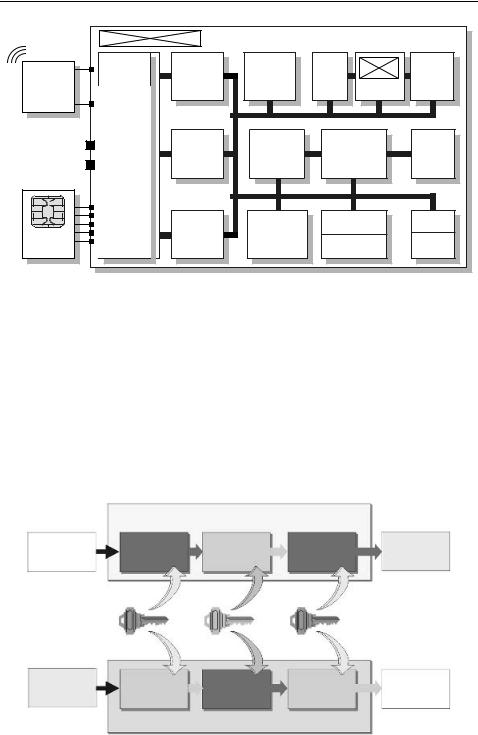
Transponders with microprocessors will become increasingly common in applications using contactless smart cards in the near future. Instead of the inflexible state machine, the transponder in these cards incorporates a microprocessor.
Industry standard microprocessors, such as the familiar 8051 or 6805, are used as the microprocessor at the heart of the chip. In addition, some manufacturers are offering simple mathematical coprocessors (cryptological unit) on the same chip, which permit the rapid performance of the calculations required for encryption procedures (Figure 10.24).
Contactless smart cards with microprocessors incorporate their own operating system, as has long been the case in contact-based cards. The tasks of the operating system in a contactless smart card are data transfer from and to the smart card, command sequence control, file management and the execution of cryptographic algorithms (e.g. encryption, authentication).
The programme modules are written in ROM code and are incorporated into the chip at the chip manufacturing stage by an additional exposure mask (mask programming).
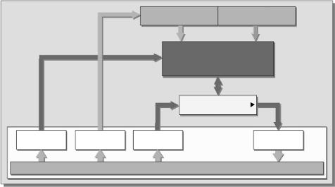
The typical command processing sequence within a smart card operating system is as follows: commands sent from the reader to the contactless smart card are received by the smart card via the HF interface. Error recognition and correction mechanisms are performed by the I/O manager irrespective of higher-level procedures. An errorfree command received by the secure messaging manager is decrypted or checked for integrity. After decryption the higher-level command interpreter attempts to decode
|
CPU |
ROM |
|
|
(Operating system) |
HF |
|
|
Interface |
Crypto |
EEPROM |
|
(Application |
|
|
|
RAM |
data) |
|
|
Transponder chip
Figure 10.24 Block diagram of a transponder with a microprocessor. The microprocessor contains a coprocessor (cryptological unit) for the rapid calculation of the cryptological algorithms required for authentication or data encryption
the command. If this is not possible, then the return code manager is called, which generates the appropriate return code and sends it back to the reader via the I/O manager (Figure 10.25).
If a valid command is received, then the actual programme code associated with this application command is executed. If access to the application data in the EEPROM is necessary, this is performed exclusively by the file management system and the memory manager, which convert all symbolic addresses into the corresponding physical addresses of the memory area. The file manager also checks access conditions (authorisation) for the data in question.
A more detailed introduction to the procedures for the development of operating systems and smart card applications can be found in the book The Smart Card Handbook published by John Wiley & Sons.
10.2.1 Dual interface card
The traditional key markets for contact smart cards are payment applications (cash card, electronic purse) and mobile telephones (SIM card for GSM mobile telephone), applications that necessitate a high degree of security in the processing and transmission
Code interpreter |
|
|
Application command |
|
|
State machine |
|
File manager |
Logical channel |
|
Memory manager |
manager |
|
|
|
Command interpreter |
|
|
Secure messaging |
Return code manager |
|
|
manager |
|
|
I/O manager |
Software |
|
HF interface |
Hardware |
EEPROM |
Figure 10.25 Command processing sequence within a smart card operating system (Rankl and Effing, 1996)
294 10 THE ARCHITECTURE OF ELECTRONIC DATA CARRIERS
of data. The resulting necessity of being able to quickly and simply calculate complex cryptographic algorithms led to the development of powerful cryptographic coprocessors on the card chips.
Contactless smart cards, on the other hand, are traditionally used in applications that require a combination of user-friendliness (access control) and short transaction times (ticketing). The trend towards combining payment applications with typical contactless applications (cash card with ticketing function) finally led to the development of the dual interface card, in which both a contact and a contactless interface are available on one chip. A dual interface card can thus be addressed either via the contactless or the contact interface.
The philosophy underlying the dual interface card is that the smart card interface is completely independent of the smart card logic or smart card software. The interface, whether contact or contactless, is completely transparent to the transmitted application data so that, from the point of view of the application software, the interface used is unimportant. The interface is thus exchangeable at will, and interface and logic components can be combined as desired. The greatest advantage of the dual interface card for the user and system operator is the option of being able to draw upon existing infrastructure (generally contact readers) when introducing new applications. Also, from the point of view of the security requirements of a smart card, there is no difference between a contact and a contactless smart card. Due to the transparency of the interface, the replay and fraud of security-related data that has been transmitted is effectively ruled out by the methods defined in ISO/IEC 7816 (e.g. ‘secure messaging’), regardless of the interface used. See Figures 10.26 and 10.27.
The greatest difference between a contactless and a contact smart card is the power available. A contactless smart card in accordance with ISO 14443 has only around 5 mW available for operation at the maximum distance from the reader (Hmin = 1.5 A/m) (Muhlbauer,¨ 2001). A contact smart card, on the other hand, may have 7.2 mW (GSM 11.13), 50 mW (GSM 11.11) or even up to 300 mW (ISO 7816-3 Class A: 5 V,
|
|
Combi-card in |
|
|
Planar Embedded Coil Technology |
|
|
|
Reinforcement and contact ring |
|
Interconnection of |
Chip module with |
Interconnection of |
|
ring with module |
contact surface |
|
ring with module |
|
|
|
Upper cover sheet |
Inlet sheet |
Lower cover sheet |
Coil wire end |
Embedded coil |
Coil wire end |
connected to ring |
|
connected to ring |
AmaTech
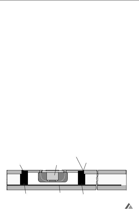
Figure 10.26 Possible layout of a dual interface smart card. The chip module is connected to both contact surfaces (like a telephone smart card) and a transponder coil (reproduced by permission of Amatech GmbH & Co. KG, Pfronten)
|
ISO 7816-2 |
|
|
|
|
UART |
RAM |
|
|
|
ROM |
|
|
|
(operating system) |
|
|
|
CPU |
|
ISO 14443-2 |
HF |
EEPROM |
|
interface |
|
|
(application data) |
|
|
(CIU) |
|
|
|
Dual interface chip
Figure 10.27 Block diagram of a dual interface card. Both smart card interfaces can be addressed independently of one another
60 mA) available depending upon its specification (Philipp, 2001). This calls for completely new concepts in the development of contactless microprocessor chips. For example, the use of a PMU (power management unit) on the chip, which can automatically separate inactive circuit parts of the chip from the power supply to save energy, is recommended. Furthermore, ultra-low-power and low-voltage technology is used in all dual interface chips so that the available power can be optimally exploited.
An explicit switching between contactless and contact operation on the chip is not necessary. In the simplest case it is sufficient to use the validity of the data received via one of the two interfaces as the evaluation criterion for further operation. Some chips provide the programmer with status flags that allow the currently active operating mode to be interrogated. Moreover, the signals (frequency, voltage) present at the HF interface or the chip contacts are evaluated.
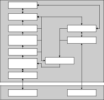
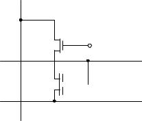
10.2.1.1MIFARE plus
The block diagram in Figure 10.28 shows a very early approach to the dual interface card. This chip was developed jointly by Philips Semiconductors Gratkorn and Siemens HL (now Infineon AG) as early as 1997. Since it was not possible using the semiconductor technologies available at the time to reliably operate a microprocessor with the power available via the contactless interface, an unconventional solution was selected.
At the heart of this chip is an 8 Kbyte EEPROM memory, the Common EEPROM, in which the application data was stored. In a similar manner to a dual port RAM, this common EEPROM can be accessed via two interfaces that are completely separate from each other from the point of view of circuitry. The inactive interface at any time is completely separated from the power supply of the chip, so that the power available in contactless operation is used optimally.
The contactless interface is based upon a state machine, which forms a contactless MIFARE memory card. From the point of view of a contactless reader this dual interface card thus behaves like a memory card with a segmented EEPROM memory,
296 |
10 THE ARCHITECTURE OF ELECTRONIC DATA CARRIERS |
Chip |
|
|
|
|
|
EEPROM |
39 |
|
0 |
|
Sector |
Common |
Sector |
|
|
|
|
|
|
EEPROM |
MIFARE® |
Inter- |
|
|
CPU |
|
|
|
interface |
face |
|
|
|
|
|
|
|
and logic |
|
|
|
|
|
RAM |
ROM |
|
Access |
|
|
configuration matrix |
|
|
|
|
Sector accessC proprietary
MIFARE® proprietary
common use for C and MIFARE®
Figure 10.28 Block diagram of the MIFARE -plus ‘dual interface card’ chip. In contactless operating mode the common EEPROM is accessed via a MIFARE -compatible state machine. When operating via the contact interface a microprocessor with its own operating system accesses the same memory (reproduced by permission of SLE 44R42, Infineon AG, Munich)
in which the arrangement of the individual segments and memory blocks are identical to that of a conventional MIFARE card (see Section 10.1.3.5).
The contact interface, on the other hand, is based upon a microprocessor with its own smart card operating system. The above-mentioned memory segmentation is once again present when the microprocessor accesses the common EEPROM. The operating system can therefore only read and write the common EEPROM in blocks within the corresponding sectors.
In addition, the write and read rights for individual memory blocks of the common EEPROM can be configured separately for the contactless and contact interface. These access rights are set in, and monitored by, the Access Configuration Matrix. This also facilitates the realisation of hierarchical security concepts.
10.2.1.2Modern concepts for the dual interface card
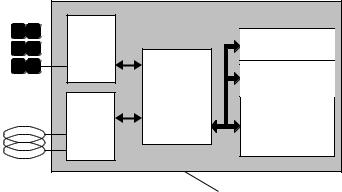
Figure 10.29 shows the block diagram of a modern dual interface card. This card is based upon a 8051 microprocessor with a smart card operating system. The contactless interface is formed by a CIU (contactless interface unit), which can be configured by the CPU via register addresses or can also facilitate a status interrogation of the CIU.
A modern CIU automatically performs the transfer of a data block from and to a reader and thereby automatically performs the necessary coding or decoding of the data stream according to the specifications in the standard ISO/I EC14443-2 and ISO/I EC14443-3. Often it also performs the automatic calculation and verification of the transmitted CRCs.
To send a data block, the operating system only needs to store the data block to be sent in the RAM memory of the chip and load the corresponding memory address and block length into the configuration register of the CIU. The CPU is no longer actively involved in the initiated data transfer and can thus be switched into power down mode
10.2 |
MICROPROCESSORS |
|
|
|
297 |
|
LA |
RF |
UART |
3DES |
|
|
|
|
interface |
RAM |
EEPROM |
|
Card coil |
|
ISO14443 |
co-processor |
PKI |
|
|
|
|
|
|
|
|
|
|
co-processor |
|
|
LB |
Security |
|
|
|
|
|
|
|
|
|
|
sensors |
|
|
|
|
|
|
Power on |
|
MMU |
|
|
|
IO2 |
reset |
|
Ultra low power |
|
|
CRC |
memory |
Interrupt |
|
|
|
80C51 |
|
|
|
generator |
management |
system |
|
IO3 |
|
compatible core |
|
Voltage |
|
unit |
|
|
|
|
|
|
|
|
regulator |
|
|
|
|
|
|
Clock |
|
|
|
|
|
|
input filter |
|
|
TIMER0 |
|
|
|
|
|
Programmable |
User-rom |
|
|
|
UART |
16 Bit |
|
ISO |
Reset |
ISO 7816 |
IO |
TIMER1 |
Test-rom |
|
contacts |
generator |
|
1,2,3 |
|
|
|
16 Bit |
|
|
|
|
|
|
|
|
|
|
|
|
|
MGa 12/01 |
Figure 10.29 Block diagram of the dual interface card chip ‘MIFARE ProX’ (reproduced by permission of Philips Semiconductors Gratkorn, A-Gratkorn)
(power saving mode) for the duration of the data transfer (Muhlbauer,¨ 2001). When a data block is received, the data from the CIU is then automatically stored in the chip’s RAM and the CRC of the received block is verified.
Short transaction times represent a particularly important requirement for contactless applications. For ticketing applications a maximum transaction time of 100 ms is a generally accepted value. In order to facilitate the calculation of cryptographic functions within this short time interval, many dual interface chips have cryptographic coprocessors. In banking applications, symmetrical encryption algorithms such as DES (data encryption standard) and triple DES are normally used (Figure 10.30). Encryption
|
Encryption sequence |
|
|
Plain data |
DES |
DES |
DES |
Cipher data |
‘Hello world’ |
encryption |
decryption |
encryption |
0x2A, 0xFA,... |
|
Key A |
Key B |
Key A |
|
Cipher data |
DES |
DES |
DES |
Plain data |
0x2A, 0xFA,... |
decryption |
encryption |
decryption |
‘Hello world’ |
Decryption sequence
Figure 10.30 Calculation of the 3DES (triple DES). Encryption (above) and decryption (below) of a data block (reproduced by permission of Philips Semiconductors Gratkorn, A-Gratkorn)
298 |
10 THE ARCHITECTURE OF ELECTRONIC DATA CARRIERS |
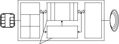
and decryption by software is time consuming and therefore not practical in a contactless application. DES encryption can be calculated several hundreds of times quicker using a coprocessor than is possible with the software solution (Muhlbauer,¨ 2001). The CPU need only enter the data to be encrypted and the key in the correct register (DDAT and DKEY in Figure 10.31) and start the calculation by means of a control register (DCNTRL).
Asymmetric key algorithms (‘public key’ procedures such as RSA) will become increasingly important in future. Typical applications are electronic signatures (digital signature) or the validity testing of electronic documents (certification). Therefore, the first dual interface chips already have coprocessors for asymmetric algorithms (e.g. Fame PKI in Figure 10.29).
10.3Memory Technology
After the state machine or microprocessor, the most important component of a data carrier is the memory that user data is read from or written to. Read-only data is defined at the manufacturing stage by the chip mask (exposure mask) or permanently burnt into the memory by a laser. The use of a laser also makes it possible to programme unique numbers (serial numbers that are issued only once) or consecutive numbers into the data carrier.
If data is to be written to the data carrier, then RAM, EEPROM or FRAM cells are also incorporated into the chip. However, only EEPROM and FRAM cells can store the written data for long periods (typical retention periods are 10 years) without a power supply.
|
|
Key A |
Key B |
|
|
8 bytes |
8 bytes |
|
|
|
|
DES |
|
|
|
|
calculation |
|
|
|
|
unit |
|
|
|
|
Data |
|
|
|
|
|
|
|
|
|
|
8 bytes |
DCNTRL |
DKEY |
DDAT |
|
DDAT |
8 bit (write only) |
8 bit (write only) |
8 bit (write) |
|
8 bit (read) |
|
|
SFR-BUS |
|
|
Figure 10.31 Block diagram of a DES coprocessor. The CPU key and data can be transferred to the coprocessor by means of its own SFR (special function register) (reproduced by permission of Philips Semiconductors Gratkorn, A-Gratkorn)
10.3 MEMORY TECHNOLOGY |
299 |
10.3.1 RAM
RAM is memory that can be used for the storage of temporary data. When the power supply is removed, the stored data is lost forever. In transponders, RAM is mainly used for the temporary storage of data that exists briefly during operation in the interrogation zone of a reader. In active transponders that have their own battery, RAMs with battery backups are sometimes used for the long-term storage of data.
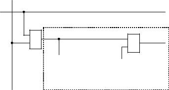
The main component of the (S)RAM memory cell is a D-flip-flop. Figure 10.32 shows the block diagram for a single memory cell. Each memory cell has the connections DI (Data Input), WE (Write Enable) and DO (Data Out). If data is only to be read from the memory cell, it is sufficient to activate the selected cell with logic 1 levels at the allocated address connections Yi and Xi.
To write data to the memory cell, the WE connection must also be switched to the 1 level. If there is a 1 level at C1 input data is written to the flip-flop.
10.3.2 EEPROM
The operating principle of an EEPROM cell is based upon the ability of a capacitor (condenser) to store electric charge over long periods. An EEPROM therefore represents a tiny capacitor that can be charged or discharged. A charged capacitor represents a logic ‘1’, a discharged capacitor represents a logic ‘0’.
In its simplest form, an EEPROM cell basically consists of a modified field effect transistor on a carrier material (substrate) made of silicon. The EEPROM cell contains an additional gate between the control gate of the field effect transistor and the substrate, which is not connected to an external power supply, and which is positioned at a very short distance ( 10 nm) from the carrier material. This so-called floating gate can be charged or discharged via the substrate using the tunnel effect, and therefore represents a capacitor. For the tunnel effect to exist there must be a sufficiently large potential difference at the thin insulating tunnelling oxidation layer between the floating gate and the substrate (Figure 10.33).
The flow of current between source and drain can be controlled by the stored charge of the floating gate. A negatively charged floating gate gives rise to a high threshold
Xi
Yi &
&
DO
Figure 10.32 Simplified functional block diagram of a (S)RAM cell
300 |
10 THE ARCHITECTURE OF ELECTRONIC DATA CARRIERS |
Bit line
Selected gate
Word line
Floating gate with 
 tunnelling oxidation layer
Pulse common plate line
Figure 10.33 The EEPROM cell consists of a modified field effect transistor with an additional floating gate
voltage between the source and drain of the field effect transistor, meaning that this is practically blocked. The current flow through the field effect transistor of an EEPROM cell is evaluated by signal amplification of the memory chip, whereby the strength of the current clearly indicates a ‘0’ or ‘1’.
To write a ‘0’ or ‘1’ to an EEPROM cell, a high positive or negative voltage is applied to the control gate, which activates the tunnel effect. The voltage required to charge the EEPROM cell is around 17 V at the control gate which falls to 12 V at the floating gate. However, RFID data carriers are supplied with 3 V or 5 V from the HF interface (or a battery). Therefore a voltage of 25 V is generated from the low supply voltage of the chip using a cascaded charging pump integrated into the chip, which provides the required 17 V after stabilisation.
It takes between 5 and 10 ms to charge an EEPROM cell. The number of possible write cycles is limited to between 10 000 and 100 000 for EEPROM cells. This is because in every write operation electrons are captured by the tunnelling oxidation layer and these are never released. These electrons influence the threshold voltage of the field effect transistor, with the effect becoming greater with every write operation. As soon as this parasitic effect of the tunnelling oxidation layer becomes greater than the primary influence of the floating gate the EEPROM cell has reached its lifetime (Rankl and Effing, 1996).
A charged floating gate loses its charge due to insulation losses and quantum mechanical effects. However, according to the semiconductor manufacturer’s figures, EEPROMs still provide reliable data retention for 10 years. If the EEPROM cell is nearing its lifetime, then information is only stored for short periods, which are determined by the parasitic influence of the oxide layer. For this reason, a plausibility test should be carried out on stored data using checksums (e.g. CRC) in RFID data carriers with EEPROM memories.
10.3.3 FRAM
High power consumption during writing and high write times of around 5–10 ms have a detrimental effect on the performance of RFID systems that employ EEPROM
10.3 MEMORY TECHNOLOGY |
301 |
technology. A new, non-transient memory technology, which should improve this situation, has been under development for around 20 years: ferroelectrical RAM, or FRAM. At the end of the 1980s the company Ramtron was established, which collaborated with Hitachi on the development of this technology. The first RFID systems using FRAM technology were produced by the Ramtron subsidiary Racom. However, the development of FRAMs is still associated with many problems, and so RFID systems using FRAMs are still not widespread.
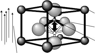
The principle underlying the FRAM cell is the ferroelectric effect, i.e. the capability of a material to retain an electrical polarisation even in the absence of an electric field. The polarisation is based upon the alignment of an elementary dipole within a crystal lattice in the ferroelectric material due to the effect of an electric field that is greater than the coercive force of the material. An opposing electric field causes the opposite alignment of the internal dipole. The alignment of the internal dipole takes on one of two stable states, which are retained after the electric field has been removed.
Figure 10.34 shows a simplified model of the ferroelectric lattice. The central atom moves into one of the two stable positions, depending upon the field direction of the external electric field. Despite this, FRAM memories are completely insensitive to foreign electric interference fields and magnetic fields.
To read the FRAM cell (Figure 10.35), an electric field (UCC) is applied to the ferroelectric capacitor via a switching transistor. If the stored information represents a logic ‘1’ then the cell is in position A on the hysteresis loop. If, on the other hand, it represents a logic ‘0’, the cell is in position C. By the application of the voltage UCC we move to point B on the hysteresis loop, releasing electric charge, which is captured and evaluated by the signal amplifiers on the memory chip. The magnitude of escaping charge clearly indicates a ‘1’ or ‘0’, because a significantly greater charge escapes in the transition from state A to B than in the transition from state C to B.
After the external (read) field UCC has been removed, the FRAM cell always returns to state C, and thus a stored ‘1’ is lost, because state C represents a ‘0’. For this reason, as soon as a ‘1’ is read, the memory chip’s logic automatically performs a rewrite operation. This involves applying an opposing electric field −UCC to the ferroelectric capacitor, which changes the state of the FRAM cell, moving it to point D on the
Divalent or monovalent metal atoms
Oxygen atoms
Tetravalent or pentavalent atom
Applied electric field
Figure 10.34 Basic configuration of a ferroelectric crystal lattice: an electric field steers the inner atom between two stable states