

Finkenzeller K.RFID handbook.2003
.pdf
 Suffix: 1st applicative command

9.2 CONTACTLESS SMART CARDS |
253 |
FSDI (frame size device integer) defines the maximum |
number of bytes that |
may be sent from the card to the reader in one block. Possible values for this are 16, 24, 32, . . . 128 and 256 bytes.
Furthermore, the smart card is allocated a CID (card identifier). Using the CID, it is possible for a reader to maintain several Type A cards in a selected state at the same time and to address an individual card selectively via its CID.
The ATS (answer to select) sent by the card in response to the RATS command corresponds with the function of the ATR (answer to reset) of a contact smart card and describes important protocol parameters of the smart card’s operating system, so that the data transmission between card and reader can be optimised in relation to the properties of the implemented application.
Individually, the (optional) parameters listed in Table 9.12 can be contained in the ATS.
Immediately after receiving the ATS, the reader can still initiate the changeover of the transmission baud rates by sending out a special PPS command (protocol parameter selection). Based upon an initial baud rate of 106 Kbit/s, the baud rates in both transmission directions can be increased independently of one another by a factor of 2, 4 or 8 if the smart card has signalled the support of higher baud rates in the optional parameters DS and DR in the ATS.
Protocol The protocol described in ISO 14443-4 supports the transmission of application data (APDU = application data unit) between the reader and the smart card. The transmitted APDU can contain any desired data, such as command and response. The structure of this protocol is based heavily upon the protocol T = 1 (ISO 7816-3) that we know from contact smart cards, in order to keep the integration of this protocol
Table 9.12 The ATS describes important protocol parameters of the Type A card
Parameters |
Comment |
|
|
FSCI |
frame size card integer: Maximum number of bytes that may be sent in a |
|
block from the reader to the card |
DS |
data rate send: Supported data rates of the smart card during the data |
|
transfer from the card to the reader (possible values: 106, 204, 408, |
|
816 Kbit/s) |
DR |
data rate send: Supported data rates of the smart card during the data |
|
transmission from the reader to the card (possible values: 106, 204, 408, |
|
816 Kbit/s) |
FWI |
frame waiting integer: This parameter defines the ‘frame waiting time’, i.e. |
|
the maximum time that a reader has to wait after transmitting a |
|
command for the response of the smart card. If no answer has been |
|
received from the card after the end of this time, then a ‘timeout’ error |
|
occurs in the communication |
SFGI |
startup frame guard integer: This parameter defines the ‘startup frame |
|
waiting time’, a special ‘frame waiting time’, that is valid exclusively for |
|
the performance of the first application command after the ATS |
CID supported |
These parameters indicate whether the parameters CID (card identifier) and |
NAD supported |
NAD (node address) are supported by the smart card’s operating system |
Historical bytes |
The historical bytes contain additional, freely definable information on the |
|
operating system of the smart card, e.g. a version number |
|
|

9.2 CONTACTLESS SMART CARDS |
255 |
PCB |
[CID] |
[NAD] |
[INF/APDU] |
CRC |
|
|
|
< FSD/FSC |
|
Figure 9.28 Structure of the frame in ISO 14443. The data of the application layer, Layer 7 (grey), are packed into the protocol frame of the transport layer (white)
b7 |
|
b6 |
b5 |
b4 |
b3 |
b2 |
b1 |
b0 |
|
|
|
|
|
|
|
|
|
|
00 |
0 |
chn |
cid |
nad |
1 |
bnr |
|
|
|
|
|
|
|
|
|
|
Block number
1 = NAD following
1 = CID following
1 = Chaining I-Block
b7 |
|
b6 |
b5 |
b4 |
b3 |
b2 |
b1 |
b0 |
|
|
|
|
|
|
|
|
|
10 |
|
0 |
ack |
cid |
0 |
1 |
bnr |
|
|
|
|
|
|
|
|
|
|
Block number
1 = CID following
1 = NAK, 0 = ACK R-Block
b7 |
|
b6 |
b5 |
|
b4 |
b3 |
b2 |
b1 |
b0 |
|
|
|
|
|
|
|
|
|
|
|
11 |
|
wtx |
cid |
0 |
1 |
0 |
||
|
|
|
|
|
|
|
|
|
|
1 = CID following
00b = Deselect, 11b = WTX S-Block
Figure 9.29 Coding of the PCB byte in a frame. The entire transmission behaviour is controlled by the PCB (protocol control byte) in the protocol
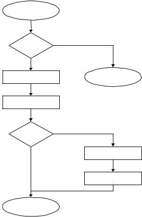
The blocks are differentiated by different coding of the PCB (protocol control byte), as shown in Figure 9.29.
The optional CID (card identifier) is used for addressing an individual smart card in the interrogation zone of the reader. Thus, several smart cards can be activated at the same time and addressed selectively using their CID. The NAD byte (node address) was introduced in order to ensure compatibility between ISO 14443-5 and ISO 7816-3 (T = 1). The use of this byte is therefore not further defined in ISO 14443.
In the case of an I block, the information field (INF) serves as a container for the data of the application layer (APDU). The content is transmitted entirely transparently. This means that the content of the protocol is forwarded directly without analysis or evaluation.
Finally, a 16-bit CRC is appended as an EDC (error detection code) for error control.
256 |
9 STANDARDISATION |
9.2.3 ISO 15693 – Vicinity coupling smart cards
The ISO standard 15693 entitled ‘Identification cards — contactless integrated circuit(s) cards — Vicinity Cards’ describes the method of functioning and operating parameters of contactless vicinity coupling smart cards. These are smart cards with a range of up to 1 m, like those used in access control systems. The data carriers used in these smart cards are predominantly cheap memory modules with simple state machines (see Section 10.1.2.1).
The standard is made up of the following parts:
•Part 1: Physical characteristics
•Part 2: Radio frequency power, signal interface and frames (still in preparation)
•Part 3: Protocols (in preparation)
•Part 4: Registration of applications/issuers (in preparation)
9.2.3.1Part 1 – Physical characteristics
Part 1 of the standard defines the mechanical properties of proximity coupling smart cards. The dimensions of the smart card correspond with those specified in ISO 7810, i.e. 85.72 mm × 54.03 mm × 0.76 mm ± tolerances.
Furthermore, this part of the standard includes additional notes for the testing of the dynamic bending stress and the dynamic torsion stress, plus irradiation with UV, x-ray and electromagnetic radiation.
9.2.3.2Part 2 – Air interface and initialisation
The power supply of the inductively coupled vicinity card (VICC ) is provided by the magnetic alternating field of a reader (PCD) at a transmission frequency of 13.56 MHz. The vicinity card incorporates a large area antenna coil for this purpose, typically with 3–6 windings of wire (see Figures 2.11 and 2.12).
The magnetic field to be generated by the reader must lie within the limit values 115 mA/m ≤ H ≤ 7.5 A/m. Thus, it is automatically the case for the interrogation field strength Hmin of a proximity coupling smart card that Hmin ≤ 115 mA/m.
Data transfer reader → card Both 10% ASK and 100% ASK modulation are used for the data transfer from a reader to a vicinity smart card (see Section 6.2.1). Regardless of the selected modulation index, moreover, one of two different coding procedures can be selected: a ‘1 of 256’ code or a ‘1 of 4’ code.
A vicinity smart card must, in principle, support both modulation and coding procedures. However, not all combinations are equally practical. For example, 10% ASK modulation in combination with ‘1 of 256’ coding should be given preference in ‘long distance mode’. The lower field strength of the modulation sidebands in comparison to the field strength of the (13.56 MHz) carrier signal in this combination permits the full exploitation of the permissible magnetic field strength for the power supply of the

9.2 CONTACTLESS SMART CARDS |
257 |
card (see FCC 15 Part 3: the permissible magnetic field strength of the modulation side bands lies 50 dB below the maximum field strength of the carrier signal of 42 dBµA/m here). By contrast, 100% ASK modulation in combination with ‘1 of 4’ coding in readers can be used with reduced range or even shielded readers (‘tunnel’ readers on conveyor belts).
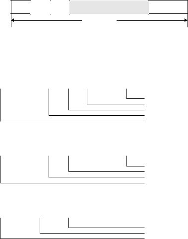
‘1 of 256’ coding This coding procedure is a pulse position modulation (PPM ) procedure. This means that the value of the digit to be transferred is unambiguously defined in the value range 0–255 by the time position of a modulation pulse (see Figure 9.30). Therefore, 8 bits (1 byte) can be transferred at the same time in one step. The total transmission time for a byte is 4.833 ms. This corresponds with 512 time slots of 9.44 µs. A modulation pulse can only take place at an uneven time slot (counting begins at zero). The value n of a transferred digit can easily be determined from the pulse position:
Pulse position = (2 · n) + 1 |
(9.1) |
The data rate resulting from the transmission period of a byte (4.833 ms) is 165 Kbit/s. The beginning and end of a data transmission are identified by defined frame signals — start-of-frame (SOF) and end-of-frame (EOF). The coding of the SOF and EOF signals selected in the standard is such that these digits cannot occur during a transmission of useful data (Figure 9.31). The unambiguity of the frame signals is thus
always ensured.
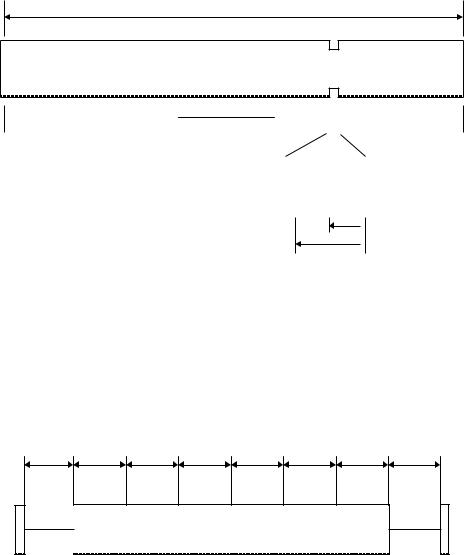
The SOF signal in ‘1 of 256’ coding consists of two 9.44 µs long modulation pulses separated by a time slot of 56.65 µs (9.44 µs × 4) (Figure 9.32).
The EOF signal consists of a single modulation pulse lasting 9.44 µs, which is sent at an even time slot in order to ensure its unambiguous differentiation from a data byte (Figure 9.33).
‘1 of 4’ coding In this coding too, the time position of a modulation pulse determines the value of a digit. Two bits are transmitted simultaneously in a single step; the value of the digit to be transferred thus lies in the value range 0–3. The total transmission time
Table 9.13 Modulation and coding procedures in ISO 15693 (Berger, 1998)
Parameter |
Value |
Comment |
|
|
|
Power supply |
13.56 MHz ± 7 kHz |
Inductive coupling |
Data transfer reader → card |
|
|
Modulation |
10% ASK, 100% ASK |
Card supports both |
Bit coding |
‘Long distance mode’: ‘1 of 256’ |
Card supports both |
|
‘Fast mode’: ‘1 of 4’ |
|
Baud rate |
‘Long distance mode’: 1.65 Kbit/s |
|
Data transfer card → reader |
‘Fast mode’: 26.48 Kbit/s |
|
|
|
|
Modulation |
Load modulation with subcarrier |
|
Bit coding |
Manchester, subcarrier is modulated |
|
|
with ASK (423 kHz) or FSK |
|
|
(423/485 kHz) |
|
Baud rate |
‘Long distance mode’: 6.62 Kbit/s |
Selected by the reader |
|
‘Fast mode’: 26.48 Kbit/s |
|
|
|
|
258 |
9 STANDARDISATION |
4.833 ms
0 |
1 |
2 |
3 |
4 |
5 |
6 |
7 |
8 |
9 |
A |
B |
|
|
|
F |
F |
|
F |
F |
|
F |
F |
F |
|
F |
F |
F |
F |
F |
F |
||||||||
|
|
2 |
|
3 |
|
4 |
|
5 |
|
6 |
|
|
8 |
|
|
|
9 |
A |
B |
C |
D |
E |
||||||||||||||||
|
|
|
|
|
|
|
|
|
|
|
|
|
|
|
|
|
|
|
|
|
|
|
||||||||||||||||
|
|
|
|
|
|
|
|
|
|
|
|
|
|
|
|
|
|
|
|
|
|
|
|
|
|
|
|
|
|
|
|
|
|
|
|
|
|
|
|
|
|
|
|
|
|
|
|
|
|
|
|
|
|
|
|
|
|
|
|
|
|
|
|
|
|
|
|
|
|
|
|
|
|
|
|
|
|
|
|
|
|
|
|
|
|
|
|
|
|
|
|
|
|
|
|
|
|
|
|
|
|
|
|
|
|
|
|
|
|
|
|
|
|
|
|
|
|
|
|
|
|
|
|
|
|
|
|
|
|
|
|
|
|
|
|
|
|
|
|
|
|
|
|
|
|
|
|
|
|
|
|
|
|
|
|
|
|
|
|
|
|
|
|
|
|
|
|
|
|
|
|
|
|
|
|
|
|
|
|
|
|
|
|
|
|
|
|
|
|
|
|
|
|
|
|
|
|
|
|
|
|
|
|
|
|
|
|
|
|
|
|
|
|
|
|
|
|
|
|
|
|
|
|
|
|
|
|
|
|
|
|
|
|
|
|
|
|
|
|
|
|
|
|
|
|
|
|
|
|
|
|
|
|
|
|
|
|
|
|
|
|
|
|
|
|
|
|
|
|
|
|
|
|
|
|
|
|
|
|
|
|
|
|
|
|
|
|
|
|
|
|
|
|
|
|
|
|
|
|
|
|
|
|
|
|
|
|
|
|
|
|
 9.44 s
 18.8 s
Figure 9.30 The ‘1 of 256’ coding is generated by the combination of 512 time slots of 9.44 µs length. The value of the digit to be transferred in the value range 0–255 can be determined from the position in time of a modulation pulse. A modulation pulse can only occur at an uneven time slot (1, 3, 5, 7, . . .)
SOF |
Byte 1 |
Byte 2 |
... |
Byte N |
EOF |
|
|
|
|
|
|
Figure 9.31 Structure of a message block (framing) made up of frame start signal (SOF), data and frame end signal (EOF)
9.44 s 9.44 s 9.44 s 9.44 s 9.44 s 9.44 s 9.44 s 9.44 s
Figure 9.32 Coding of the SOF signal at the beginning of a data transmission using ‘1 of 256’ coding
for a byte is 75.52 µs, which corresponds with eight time slots of 9.44 µs. A modulation pulse can only be transmitted at an uneven time slot (counting begins at zero). The value n of a transmitted figure can easily be determined from the pulse position:
Pulse position = (2 · n) + 1 |
(9.2) |
The data rate resulting from the time taken to transmit a byte |
(75.52 µs) is |
26.48 Kbit/s. |
|

9.2 CONTACTLESS SMART CARDS |
|
|
|
|
|
259 |
||||||||||
|
|
|
9.44 s |
|
|
9.44 s |
|
9.44 s |
|
9.44 s |
||||||
|
|
|
|
|
|
|
|
|
|
|
|
|
|
|
|
|
|
|
|
|
|
|
|
|
|
|
|
|
|
|
|
|
|
|
|
|
|
|
|
|
|
|
|
|
|
|
|
|
|
|
|
|
|
|
|
|
|
|
|
|
|
|
|
|
|
|
|
|
|
|
|
|
|
|
|
|
|
|
|
|
|
|
|
|
Figure 9.33 The EOF signal consists of a modulation pulse at an even time slot (t = 2) and thus is clearly differentiated from useful data
|
|
9.44 s |
|
|
9.44 s |
|
|
9.44 s |
|
|
9.44 s |
|
|
9.44 s |
|
9.44 s 9.44 s |
9.44 s |
|
|||||||
|
|
|
|
|
|
|
|
|
|
|
|
|
|
|
|
|
|
|
|
|
|
|
|
|
|
|
|
|
|
|
|
|
|
|
|
|
|
|
|
|
|
|
|
|
|
|
|
|
|
|
|
|
|
|
|
|
|
|
|
|
|
|
|
|
|
|
|
|
|
|
|
|
|
|
|
|
|
|
|
|
|
|
|
|
|
|
|
|
|
|
|
|
|
|
|
|
|
|
|
|
|
|
|
Figure 9.34 The SOF signal of ‘1 of 4’ coding consists of two 9.44 µs long modulation pulses separated by an interval of 18.88 µs
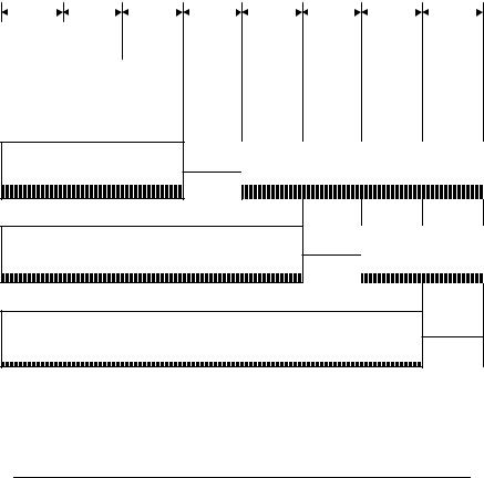
In ‘1 of 4’ coding the SOF signal is made up of two modulation pulses lasting 9.44 µs separated by an interval of 37.76 µs (Figure 9.34). The first digit of the useful data begins after an additional pause of 18.88 µs after the second modulation pulse of the SOF signal. See Figure 9.35.
The conclusion of the transmission is identified by the familiar frame end signal (EOF).
Data transfer card → reader Load modulation with a modulated subcarrier is used for the data transfer from a vicinity card to a reader. The ohmic or capacitive modulation resistor is switched on and off in time with the subcarrier frequency. The subcarrier itself is modulated in time with the Manchester coded data stream, using ASK or FSK modulation (Table 9.14). The modulation procedure is selected by the reader using a flag bit (control bit) in the header of the transmission protocol defined in Part 3 of the standard. Therefore, in this case too, both procedures must be supported by the smart card.
The data rate can also be switched between two values (Table 9.15). The reader selects the data rate by means of a flag bit (control bit) in the header of the transmission protocol, which means that, in this case too, the card must support both procedures.
Table 9.14 Subcarrier frequencies for an ASK and FSK modulated subcarrier
|
ASK ‘on-off keying’ |
FSK |
|
|
|
Subcarrier frequency |
423.75 kHz |
423.75 kHz/484.28 kHz |
Divider ratio to fc = 13.56 MHz |
fc/32 |
fc/32; fc/28 |
260 |
|
|
|
|
|
|
|
|
|
|
|
|
|
|
|
9 STANDARDISATION |
|||||
|
|
9.44 s 9.44 s 9.44 s |
9.44 s 9.44 s 9.44 s 9.44 s 9.44 s |
||||||||||||||||||
|
|
|
|
|
|
|
|
|
|
|
|
|
|
|
|
|
|
|
|
|
|
|
Pulse position for 00 |
|
|
|
|
|
|
|
|
|
|
|
|||||||||
|
|
|
|
|
|
|
|
|
|
|
|
|
|
|
|
|
|
|
|
|
|
|
|
|
|
|
|
|
|
|
|
|
|
|
|
|
|
|
|
|
|
|
|
|
|
|
|
|
|
|
|
|
|
|
|
|
|
|
|
|
|
|
|
|
|
|
|
|
|
|
|
|
|
|
|
|
|
|
|
|
|
|
|
|
|
|
|
Pulse position for 01
Pulse position for 10
Pulse position for 11
Figure 9.35 ‘1 of 4’ coding arises from the combination of eight time slots of 9.44 µs length. The value of the digit to be transmitted in the value range 0–3 can be determined from the time position of a modulation pulse
Table 9.15 Data rates of the two transmission modes
Data rate |
ASK (‘on-off keying’) |
FSK |
|
|
|
‘Long distance mode’ |
6.62 Kbit/s |
6.62 Kbit/s/6.68 Kbit/s |
‘Fast mode’ |
26.48 Kbit/s |
26.48 Kbit/s/26.72 Kbit/s |
|
|
|
9.2.4ISO 10373 – Test methods for smart cards
ISO 10373 provided a standard relating to the testing of cards with and without a chip. In addition to tests for the general quality characteristics, such as bending stiffness, resistance to chemicals, dynamic torsional stress, flammability, and dimensions of cards or the ultra-violet light resistance of the data carrier (since EEPROM memories lose their content when irradiated with UV light a special test has been developed to ensure non-sensitivity to this), specific test procedures have also been developed for the latest methods of data transmission or storage (magnetic strips, contact, contactless, optical). The individual test procedures for testing magnetic strips (ISO 7811), contact smart cards (ISO 7816) or contactless smart cards (ISO 14443, ISO 15693) were summarised in independent parts of the standard for the sake of providing an overview (Table 9.16). However, in this section we will deal exclusively with the parts of the standard that are relevant to RFID systems, i.e. Part 4, Part 6 and Part 7.