

Finkenzeller K.RFID handbook.2003
.pdfRFID Handbook: Fundamentals and Applications in Contactless Smart Cards and Identification, Second Edition
Klaus Finkenzeller Copyright 2003 John Wiley & Sons, Ltd.
ISBN: 0-470-84402-7
10
The Architecture
of Electronic Data Carriers
Before we describe the functionality of the data carriers used in RFID systems we must first differentiate between two fundamental operating principles: there are electronic data carriers based upon integrated circuits (microchips) and data carriers that exploit physical effects for data storage. Both 1-bit transponders and surface wave components belong to the latter category.
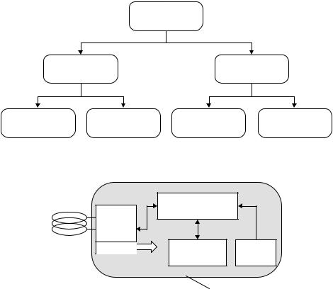
Electronic data carriers are further subdivided into data carriers with a pure memory function and those that incorporate a programmable microprocessor (Figure 10.1).
This chapter deals exclusively with the functionality of electronic data carriers. The simple functionality of physical data carriers has already been described in Chapter 3.
10.1Transponder with Memory Function
Transponders with a memory function range from the simple read-only transponder to the high end transponder with intelligent cryptological functions (Figure 10.2).
Transponders with a memory function contain RAM, ROM, EEPROM or FRAM and an HF interface to provide the power supply and permit communication with the reader. The main distinguishing characteristic of this family of transponders is the realisation of address and security logic on the chip using a state machine.
10.1.1 HF interface
The HF interface forms the interface between the analogue, high frequency transmission channel from the reader to the transponder and the digital circuitry of the transponder. The HF interface therefore performs the functions of a classical modem (modulator–demodulator) used for analogue data transmission via telephone lines.
The modulated HF signal from the reader is reconstructed in the HF interface by demodulation to create a digital serial data stream for reprocessing in the address and security logic. A clock-pulse generation circuit generates the system clock for the data carrier from the carrier frequency of the HF field.
274 |
10 THE ARCHITECTURE OF ELECTRONIC DATA CARRIERS |
Data carriers for
RFID applications
Electronic |
Physical |
circuits (IC) |
effects |
State machine |
(Programmable) |
1-bit transponder |
SAW |
|
memory |
microprocessor |
components |
||
|
Figure 10.1 Overview of the different operating principles used in RFID data carriers
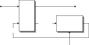
Address and HF security logic
interface
Vcc |
EEPROM |
ROM |
|
or FRAM |
|
|
|
Chip
Figure 10.2 Block diagram of an RFID data carrier with a memory function
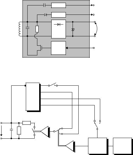
The HF interface incorporates a load modulator or backscatter modulator (or an alternative procedure, e.g. frequency divider), controlled by the digital data being transmitted, to return data to the reader (Figure 10.3).
Passive transponders, i.e. transponders that do not have their own power supply, are supplied with energy via the HF field of the reader. To achieve this, the HF interface draws current from the transponder antenna, which is rectified and supplied to the chip as a regulated supply voltage.
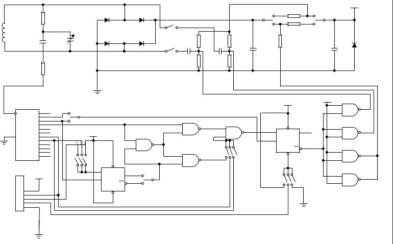
10.1.1.1Example circuit – load modulation with subcarrier
The principal basic circuit of a load modulator is shown in Figure 10.4. This generates an ohmic load modulation using an ASK or FSK modulated subcarrier. The frequency of the subcarrier and the baud rates are in accordance with the specifications of the standard ISO 15693 (Vicinity coupling smart cards).
The high-frequency input voltage u2 of the data carrier (transponder chip) serves as the time basis of the HF interface and is passed to the input of a binary divider.
10.1 TRANSPONDER WITH MEMORY FUNCTION |
275 |
Clock |
|
System clock |
Demod. |
|
Data input |
Rectifier |
ZD |
Vcc |
ASK |
|
Data input |
Load |
|
|
modulator |
|
|
Figure 10.3 Block diagram of the HF interface of an inductively coupled transponder with a load modulator
ASK/FSK
fc = 13.56 MHz
fc /28
fc /32
1/n
fc /512 fc /2048
|
Rmod |
|
u2 |
Baudrate 6.62/26.48 Kbit/s |
|
|
|
|
C2 |
RL |
|
|
S |
|
|
Manchester |
TX data |
|
generator |
buffer |
Figure 10.4 Generation of a load modulation with modulated subcarrier: the subcarrier frequency is generated by a binary division of the carrier frequency of the RFID system. The subcarrier signal itself is initially ASK or FSK modulated (switch position ASK/FSK) by the Manchester coded data stream, while the modulation resistor in the transponder is finally switched on and off in time with the modulated subcarrier signal
The frequencies specified in the standard for the subcarrier and the baud rate can be derived from the single binary division of the 13.56 MHz input signal (Table 10.1).
The serial data to be transmitted is first transferred to a Manchester generator. This allows the baud rate of the baseband signal to be adjusted between two values. The Manchester coded baseband signal is now used to switch between the two subcarrier frequencies f1 and f2 using the ‘1’ and ‘0’ levels of the signal, in order to generate an FSK modulated subcarrier signal. If the clock signal f2 is interrupted, this results in an ASK modulated subcarrier signal, which means that it is very simple to switch

276 10 THE ARCHITECTURE OF ELECTRONIC DATA CARRIERS
Table 10.1 The clock frequencies required in the HF interface are generated by the binary division of the 13.56 MHz carrier signal
Splitter N |
Frequency |
Use |
|
|
|
1/28 |
485 kHz |
φ2 of the FSK subcarrier |
1/32 |
423 kHz |
φ1 of the FSK subcarrier, plus |
|
|
ASK subcarrier |
1/512 |
26.48 kHz |
Bit clock signal for high baud rate |
1/2048 |
6.62 kHz |
Bit clock signal for slow baud rate |
|
|
|
between ASK and FSK modulation. The modulated subcarrier signal is now transferred to switch S, so that the modulation resistor of the load modulator can be switched on and off in time with the subcarrier frequency.
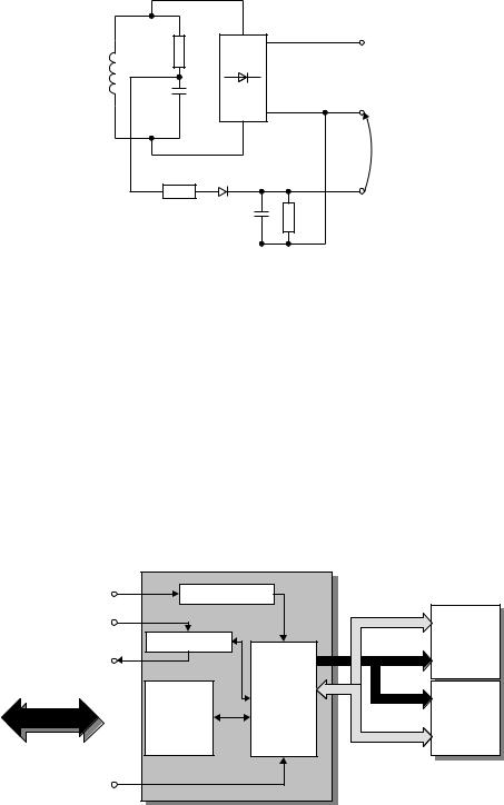
10.1.1.2Example circuit – HF interface for ISO 14443 transponder
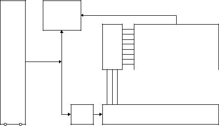
The circuit in Figure 10.5 provides a further example of the layout of a HF interface. This was originally a simulator for contactless smart cards in accordance with ISO 14443, which can be used to simulate the data transmission from the smart card to a reader by load modulation. The circuit was taken from a proposal by Motorola for a contactless smart card in ISO 10373-6 (Baddeley and Ruiz, 1998).
A complete layout is available for the duplication of this test card (see Section 14.4.1). The circuit is built upon an FR4 printed circuit board. The transponder coil is realised in the form of a large area conductor loop with four windings of a printed conductor. The dimensions of the transponder coil correspond with the ratios in a real smart card.
The transponder resonant circuit of the test card is made up of the transponder coil L1 and the trimming capacitor CV1. The resonant frequency of the transponder resonant circuit should be tuned to the transmission frequency of the reader, 13.56 MHz (compare Section 4.1.11.2). The HF voltage present at the transponder resonant circuit is rectified in the bridge rectifier D1 –D4 and maintained at approximately 3 V by the zener diode D6 for the power supply to the test card.
The binary divider U1 derives the required system clocks of 847.5 kHz (subcarrier, divider 1/16) and 105.93 kHz (baud rate, divider 1/128) from the carrier frequency 13.56 MHz.
The circuit made up of U2 and U3 is used for the ASK or BPSK modulation of the subcarrier signal (847.5 kHz) with the Manchester or NRZ coded data stream (jumper 1–4). In addition to the simple infinite bit sequences 1111 and 1010, the supply of an external data stream (jumper 10) is also possible. The test smart card thus supports both procedures for data transfer between smart card and reader defined in ISO 14443-2.
Either a capacitive (C4, C5) or an ohmic (R9) load modulation can be selected. The ‘open collector’ driver U4 serves as the output stage (‘switch’) for the load modulator.
The demodulation of a data stream transmitted from the reader is not provided in this circuit. However, a very simple extension of the circuit (see Figure 10.6) facilitates the demodulation of at least a 100% ASK modulated signal. This requires only an
280 |
10 THE ARCHITECTURE OF ELECTRONIC DATA CARRIERS |
Power
on
S1
X1
X1
S0 |
X2 |
X1 |
X2
X1 S2
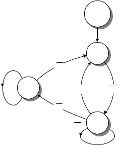
Figure 10.9 Example of a simple state diagram to describe a state machine
A switching network performs the required classification: If the state variable Z(t ) and the input variable are fed into its inputs, then the new state Z(t + 1) will occur at the output (Figure 10.8). When the next timing signal is received this state is transferred to the output of (transition triggered) flip-flops and thus becomes the new system state S(t + 1) of the state machine.
10.1.3 Memory architecture
10.1.3.1Read-only transponder
This type of transponder represents the low-end, low-cost segment of the range of RFID data carriers. As soon as a read-only transponder enters the interrogation zone of a reader it begins to continuously transmit its own identification number (Figure 10.10). This identification number is normally a simple serial number of a few bytes with a check digit attached. Normally, the chip manufacturer guarantees that each serial number is only used once. More complex codes are also possible for special functions.
The transponder’s unique identification number is incorporated into the transponder during chip manufacture. The user cannot alter this serial number, nor any data on the chip.
Communication with the reader is unidirectional, with the transponder sending its identification number to the reader continuously. Data transmission from the reader to the transponder is not possible. However, because of the simple layout of the data carrier and reader, read-only transponders can be manufactured extremely cheaply.
Read-only transponders are used in price-sensitive applications that do not require the option of storing data in the transponder. The classic fields of application are
 PSK
PSK
