

- •Universal Serial Bus Features:
- •Power-Managed Modes:
- •Flexible Oscillator Structure:
- •Peripheral Highlights:
- •Special Microcontroller Features:
- •Pin Diagrams
- •Pin Diagrams (Continued)
- •Table of Contents
- •Most Current Data Sheet
- •Errata
- •Customer Notification System
- •1.0 Device Overview
- •1.1 New Core Features
- •1.1.1 nanoWatt Technology
- •1.1.2 Universal Serial Bus (USB)
- •1.1.3 Multiple Oscillator Options and Features
- •1.2 Other Special Features
- •1.3 Details on Individual Family Members
- •FIGURE 1-2: PIC18F4455/4550 (40/44-Pin) Block Diagram
- •2.0 Oscillator Configurations
- •2.1 Overview
- •2.1.1 Oscillator Control
- •2.2 Oscillator Types
- •2.2.1 Oscillator Modes and USB Operation
- •2.2.2 Crystal Oscillator/Ceramic Resonators
- •FIGURE 2-2: Crystal/Ceramic Resonator Operation (XT, HS or HSPLL Configuration)
- •TABLE 2-1: Capacitor Selection for Ceramic Resonators
- •TABLE 2-2: Capacitor Selection for Crystal Oscillator
- •FIGURE 2-3: External Clock Input Operation (HS Osc Configuration)
- •2.2.3 External Clock Input
- •FIGURE 2-5: External Clock Input Operation (ECIO and ECPIO Configuration)
- •2.2.4 PLL Frequency Multiplier
- •FIGURE 2-6: PLL Block Diagram (HS Mode)
- •2.2.5 Internal Oscillator Block
- •2.3 Oscillator Settings for USB
- •2.3.2 Running Different USB and Microcontroller Clocks
- •2.4 Clock Sources and Oscillator Switching
- •2.4.1 Oscillator Control Register
- •2.4.2 Oscillator Transitions
- •3.0 Power-Managed Modes
- •3.1.1 Clock Sources
- •TABLE 3-1: Power-Managed Modes
- •3.1.3 Clock Transitions and Status Indicators
- •3.1.4 Multiple Sleep Commands
- •3.2 Run Modes
- •3.2.1 PRI_RUN Mode
- •3.2.2 SEC_RUN Mode
- •FIGURE 3-1: Transition Timing for Entry to SEC_RUN Mode
- •FIGURE 3-2: Transition Timing From SEC_RUN Mode to PRI_RUN Mode (HSPLL)
- •3.2.3 RC_RUN Mode
- •FIGURE 3-4: Transition Timing From RC_RUN Mode to PRI_RUN Mode
- •3.3 Sleep Mode
- •3.4 Idle Modes
- •FIGURE 3-5: Transition Timing for Entry to Sleep Mode
- •FIGURE 3-6: Transition Timing for Wake From Sleep (HSPLL)
- •3.4.1 PRI_IDLE Mode
- •3.4.2 SEC_IDLE Mode
- •FIGURE 3-7: Transition Timing for Entry to Idle Mode
- •FIGURE 3-8: Transition Timing for Wake From Idle to Run Mode
- •3.4.3 RC_IDLE Mode
- •3.5 Exiting Idle and Sleep Modes
- •3.5.1 Exit By Interrupt
- •3.5.3 Exit By Reset
- •TABLE 3-2: Exit Delay on Wake-up By Reset From Sleep Mode or Any Idle Mode (By Clock Sources)
- •4.0 Reset
- •4.1 RCON Register
- •FIGURE 4-1: Simplified Block Diagram of On-Chip Reset Circuit
- •4.2 Master Clear Reset (MCLR)
- •FIGURE 4-2: External Power-on Reset Circuit (for Slow Vdd Power-up)
- •4.4.1 Software Enabled BOR
- •4.4.2 Detecting BOR
- •4.4.3 Disabling BOR in Sleep Mode
- •TABLE 4-1: BOR Configurations
- •4.5 Device Reset Timers
- •FIGURE 4-3: Time-out Sequence on Power-up (MCLR Tied to Vdd, Vdd Rise < Tpwrt)
- •FIGURE 4-4: Time-out Sequence on Power-up (MCLR Not Tied to Vdd): Case 1
- •FIGURE 4-5: Time-out Sequence on Power-up (MCLR Not Tied to Vdd): Case 2
- •FIGURE 4-6: Slow Rise Time (MCLR Tied to Vdd, Vdd Rise > Tpwrt)
- •FIGURE 4-7: Time-out Sequence on POR w/PLL Enabled (MCLR Tied to Vdd)
- •4.6 Reset State of Registers
- •5.0 Memory Organization
- •5.1 Program Memory Organization
- •FIGURE 5-1: Program Memory Map and Stack for PIC18F2455/2550/4455/4550 Devices
- •5.1.1 Program Counter
- •5.1.2 Return Address Stack
- •FIGURE 5-2: Return Address Stack and Associated Registers
- •5.1.3 Fast Register Stack
- •5.2 PIC18 Instruction Cycle
- •5.2.1 Clocking Scheme
- •5.2.2 Instruction Flow/Pipelining
- •5.2.3 Instructions in Program Memory
- •EXAMPLE 5-4: Two-Word Instructions
- •5.3 Data Memory Organization
- •5.3.2 Bank Select Register (BSR)
- •FIGURE 5-5: Data Memory Map for PIC18F2455/2550/4455/4550 Devices
- •FIGURE 5-6: Use of the Bank Select Register (Direct Addressing)
- •5.3.3 Access Bank
- •5.3.4 General Purpose Register File
- •5.3.5 Special Function Registers
- •5.3.6 Status Register
- •5.4 Data Addressing Modes
- •5.4.1 Inherent and Literal Addressing
- •5.4.2 Direct Addressing
- •5.4.3 Indirect Addressing
- •FIGURE 5-7: Indirect Addressing
- •5.5 Program Memory and the Extended Instruction Set
- •5.6 Data Memory and the Extended Instruction Set
- •5.6.1 Indexed Addressing with Literal Offset
- •5.6.2 Instructions Affected By Indexed Literal Offset Mode
- •5.6.3 Mapping the Access Bank in Indexed Literal Offset Mode
- •5.6.4 BSR in Indexed Literal Offset Mode
- •FIGURE 5-9: Remapping the Access Bank with Indexed Literal Offset Addressing
- •6.0 Flash Program Memory
- •6.1 Table Reads and Table Writes
- •FIGURE 6-2: Table Write Operation
- •6.2 Control Registers
- •6.2.1 EECON1 and EECON2 Registers
- •6.2.2 Table Latch Register (TABLAT)
- •6.2.3 Table Pointer Register (TBLPTR)
- •6.2.4 Table Pointer Boundaries
- •FIGURE 6-3: Table Pointer Boundaries Based on Operation
- •6.3 Reading the Flash Program Memory
- •FIGURE 6-4: Reads From Flash Program Memory
- •6.4 Erasing Flash Program Memory
- •6.4.1 Flash Program Memory Erase Sequence
- •6.5 Writing to Flash Program Memory
- •FIGURE 6-5: Table Writes to Flash Program Memory
- •6.5.1 Flash Program Memory Write Sequence
- •EXAMPLE 6-3: Writing to Flash Program Memory (Continued)
- •6.5.2 Write Verify
- •6.5.3 Unexpected Termination of Write Operation
- •6.5.4 Protection Against Spurious Writes
- •6.6 Flash Program Operation During Code Protection
- •7.0 Data EEPROM Memory
- •7.1 EECON1 and EECON2 Registers
- •7.2 Reading the Data EEPROM Memory
- •7.3 Writing to the Data EEPROM Memory
- •7.4 Write Verify
- •EXAMPLE 7-1: Data EEPROM Read
- •7.6 Protection Against Spurious Write
- •7.7 Using the Data EEPROM
- •TABLE 7-1: Registers Associated with Data EEPROM Memory
- •8.0 8 x 8 Hardware Multiplier
- •8.1 Introduction
- •8.2 Operation
- •EQUATION 8-1: 16 x 16 Unsigned Multiplication Algorithm
- •EQUATION 8-2: 16 x 16 Signed Multiplication Algorithm
- •9.0 Interrupts
- •9.1 USB Interrupts
- •FIGURE 9-1: Interrupt Logic
- •9.2 INTCON Registers
- •9.3 PIR Registers
- •9.4 PIE Registers
- •9.5 IPR Registers
- •9.6 RCON Register
- •9.7 INTn Pin Interrupts
- •9.8 TMR0 Interrupt
- •9.10 Context Saving During Interrupts
- •10.0 I/O Ports
- •FIGURE 10-1: Generic I/O Port Operation
- •10.1 PORTA, TRISA and LATA Registers
- •EXAMPLE 10-1: Initializing PORTA
- •10.2 PORTB, TRISB and LATB Registers
- •EXAMPLE 10-2: Initializing PORTB
- •10.3 PORTC, TRISC and LATC Registers
- •TABLE 10-6: Summary of Registers Associated with PORTC
- •10.4 PORTD, TRISD and LATD Registers
- •10.5 PORTE, TRISE and LATE Registers
- •TABLE 10-9: PORTE I/O Summary
- •TABLE 10-10: Summary of Registers Associated with PORTE
- •11.0 Timer0 Module
- •11.1 Timer0 Operation
- •11.3 Prescaler
- •11.3.1 Switching Prescaler Assignment
- •11.4 Timer0 Interrupt
- •TABLE 11-1: Registers Associated with Timer0
- •12.0 Timer1 Module
- •12.1 Timer1 Operation
- •FIGURE 12-2: Timer1 Block Diagram (16-bit Read/Write Mode)
- •12.3 Timer1 Oscillator
- •12.3.1 Using Timer1 as a Clock Source
- •12.3.3 Timer1 Oscillator Layout Considerations
- •FIGURE 12-4: Oscillator Circuit with Grounded Guard Ring
- •12.4 Timer1 Interrupt
- •12.5 Resetting Timer1 Using the CCP Special Event Trigger
- •TABLE 12-2: Registers Associated with Timer1 as a Timer/Counter
- •13.0 Timer2 Module
- •13.1 Timer2 Operation
- •13.2 Timer2 Interrupt
- •13.3 TMR2 Output
- •TABLE 13-1: Registers Associated with Timer2 as a Timer/Counter
- •14.0 Timer3 Module
- •14.1 Timer3 Operation
- •14.3 Using the Timer1 Oscillator as the Timer3 Clock Source
- •14.4 Timer3 Interrupt
- •14.5 Resetting Timer3 Using the CCP Special Event Trigger
- •TABLE 14-1: Registers Associated with Timer3 as a Timer/Counter
- •15.0 Capture/Compare/PWM (CCP) Modules
- •Register 15-1: CCPxCON: Standard CCPx Control Register
- •15.1 CCP Module Configuration
- •15.1.1 CCP Modules and Timer Resources
- •TABLE 15-1: CCP Mode – Timer Resource
- •15.1.2 CCP2 Pin Assignment
- •TABLE 15-2: Interactions Between CCP1 and CCP2 for Timer Resources
- •15.2 Capture Mode
- •15.2.1 CCP Pin Configuration
- •15.2.2 Timer1/Timer3 Mode Selection
- •15.2.3 Software Interrupt
- •15.2.4 CCP Prescaler
- •EXAMPLE 15-1: Changing Between Capture Prescalers (CCP2 Shown)
- •FIGURE 15-1: Capture Mode Operation Block Diagram
- •15.3 Compare Mode
- •15.3.1 CCP Pin Configuration
- •15.3.2 Timer1/Timer3 Mode Selection
- •15.3.3 Software Interrupt Mode
- •15.3.4 Special Event Trigger
- •FIGURE 15-2: Compare Mode Operation Block Diagram
- •TABLE 15-3: Registers Associated with Capture, Compare, Timer1 and Timer3
- •15.4 PWM Mode
- •FIGURE 15-3: Simplified PWM Block Diagram
- •15.4.1 PWM Period
- •EQUATION 15-1:
- •15.4.2 PWM Duty Cycle
- •EQUATION 15-2:
- •EQUATION 15-3:
- •TABLE 15-4: Example PWM Frequencies and Resolutions at 40 MHz
- •15.4.4 Setup for PWM Operation
- •16.0 Enhanced Capture/Compare/PWM (ECCP) Module
- •Register 16-1: CCP1CON: ECCP Control Register (40/44-Pin Devices)
- •16.1 ECCP Outputs and Configuration
- •16.1.1 ECCP Modules and Timer Resources
- •16.2 Capture and Compare Modes
- •16.2.1 Special Event Trigger
- •16.3 Standard PWM Mode
- •TABLE 16-1: Pin Assignments for Various ECCP1 Modes
- •16.4 Enhanced PWM Mode
- •16.4.1 PWM Period
- •EQUATION 16-1:
- •FIGURE 16-1: Simplified Block Diagram of the Enhanced PWM Module
- •16.4.2 PWM Duty Cycle
- •EQUATION 16-2:
- •EQUATION 16-3:
- •16.4.3 PWM Output Configurations
- •TABLE 16-2: Example PWM Frequencies and Resolutions at 40 MHz
- •FIGURE 16-2: PWM Output Relationships (Active-High State)
- •FIGURE 16-3: PWM Output Relationships (Active-Low State)
- •FIGURE 16-4: Half-Bridge PWM Output
- •FIGURE 16-5: Examples of Half-Bridge Output Mode Applications
- •FIGURE 16-6: Full-Bridge PWM Output
- •FIGURE 16-7: Example of Full-Bridge Application
- •FIGURE 16-9: PWM Direction Change at Near 100% Duty Cycle
- •Register 16-2: ECCP1DEL: PWM Dead-Band Delay Register
- •Register 16-3: ECCP1AS: Enhanced Capture/Compare/PWM Auto-Shutdown Control Register
- •FIGURE 16-10: PWM Auto-Shutdown (PRSEN = 1, Auto-Restart Enabled)
- •FIGURE 16-11: PWM Auto-Shutdown (PRSEN = 0, Auto-Restart Disabled)
- •16.4.9 Setup for PWM Operation
- •16.4.11 Effects of a Reset
- •TABLE 16-3: Registers Associated with ECCP Module And Timer1 to Timer3
- •17.0 Universal Serial Bus (USB)
- •17.1 Overview of the USB Peripheral
- •17.2 USB Status and Control
- •17.2.1 USB Control Register (UCON)
- •Register 17-1: UCON: USB Control Register
- •17.2.2 USB Configuration Register (UCFG)
- •FIGURE 17-2: Typical External Transceiver with Isolation
- •Register 17-2: UCFG: USB Configuration Register
- •FIGURE 17-3: External Circuitry
- •17.2.3 USB Status Register (USTAT)
- •Register 17-3: USTAT: USB Status Register
- •17.2.4 USB Endpoint Control
- •Register 17-4: UEPn: USB Endpoint n Control Register (UEP0 Through UEP15)
- •17.2.5 USB Address Register (UADDR)
- •17.2.6 USB Frame Number Registers (UFRMH:UFRML)
- •FIGURE 17-5: Implementation of USB RAM in Data Memory Space
- •17.4 Buffer Descriptors and the Buffer Descriptor Table
- •17.4.1 BD Status and Configuration
- •FIGURE 17-6: Example of a Buffer Descriptor
- •TABLE 17-3: Effect of DTSEN Bit on Odd/Even (DATA0/DATA1) Packet Reception
- •17.4.2 BD Byte Count
- •17.4.3 BD Address Validation
- •FIGURE 17-7: Buffer Descriptor Table Mapping for Buffering Modes
- •TABLE 17-4: Assignment of Buffer Descriptors for the Different Buffering Modes
- •TABLE 17-5: Summary of USB Buffer Descriptor Table Registers
- •17.5 USB Interrupts
- •17.5.1 USB Interrupt Status Register (UIR)
- •Register 17-7: UIR: USB Interrupt Status Register
- •EXAMPLE 17-1: Clearing ACTVIF Bit (UIR<2>)
- •17.5.2 USB Interrupt Enable Register (UIE)
- •Register 17-8: UIE: USB Interrupt Enable Register
- •17.5.3 USB Error Interrupt Status Register (UEIR)
- •Register 17-9: UEIR: USB Error Interrupt Status Register
- •17.5.4 USB Error Interrupt Enable Register (UEIE)
- •Register 17-10: UEIE: USB Error Interrupt Enable Register
- •17.6 USB Power Modes
- •17.6.1 Bus Power Only
- •FIGURE 17-10: Bus Power Only
- •FIGURE 17-11: Self-power Only
- •FIGURE 17-12: Dual Power Example
- •17.7 Streaming Parallel Port
- •17.8 Oscillator
- •17.9 USB Firmware and Drivers
- •TABLE 17-6: Registers Associated with USB Module Operation(1)
- •17.10 Overview of USB
- •17.10.1 Layered Framework
- •17.10.2 Frames
- •17.10.3 Transfers
- •17.10.4 Power
- •FIGURE 17-13: USB Layers
- •17.10.5 Enumeration
- •17.10.6 Descriptors
- •17.10.7 Bus Speed
- •17.10.8 Class Specifications and Drivers
- •18.0 Streaming Parallel Port
- •18.1 SPP Configuration
- •18.1.1 Enabling the SPP
- •Register 18-1: SPPCON: SPP Control Register
- •Register 18-2: SPPCFG: SPP Configuration Register
- •18.1.2 Clocking Data
- •18.1.3 Wait States
- •FIGURE 18-2: Timing for Microcontroller Write Address, Write Data and Read Data (No Wait States)
- •FIGURE 18-3: Timing for USB Write Address and Data (4 Wait States)
- •FIGURE 18-4: Timing for USB Write Address and Read Data (4 Wait States)
- •18.2 Setup for USB Control
- •18.3 Setup for Microcontroller Control
- •18.3.1 SPP Interrupts
- •18.3.2 Writing to the SPP
- •FIGURE 18-5: Transfer of Data Between USB SIE and SPP
- •18.3.3 Reading From the SPP
- •Register 18-3: SPPEPS: SPP Endpoint Address and Status Register
- •TABLE 18-1: Registers Associated with the Streaming Parallel Port
- •19.0 Master Synchronous Serial Port (MSSP) Module
- •19.1 Master SSP (MSSP) Module Overview
- •19.2 Control Registers
- •19.3 SPI Mode
- •19.3.1 Registers
- •Register 19-2: SSPCON1: MSSP Control Register 1 (SPI Mode)
- •19.3.2 Operation
- •19.3.3 Enabling SPI I/O
- •19.3.4 Typical Connection
- •19.3.5 Master Mode
- •FIGURE 19-3: SPI Mode Waveform (Master Mode)
- •19.3.6 Slave Mode
- •19.3.7 Slave Select Synchronization
- •FIGURE 19-4: Slave Synchronization Waveform
- •FIGURE 19-5: SPI Mode Waveform (Slave Mode with CKE = 0)
- •FIGURE 19-6: SPI Mode Waveform (Slave Mode with CKE = 1)
- •19.3.9 Effects of a Reset
- •19.3.10 Bus Mode Compatibility
- •TABLE 19-1: SPI Bus Modes
- •TABLE 19-2: Registers Associated with SPI Operation
- •FIGURE 19-7: MSSP Block Diagram (I2C™ Mode)
- •19.4.1 Registers
- •19.4.2 Operation
- •19.4.3 Slave Mode
- •EXAMPLE 19-2: Address Masking Examples
- •19.4.4 Clock Stretching
- •FIGURE 19-14: Clock Synchronization Timing
- •19.4.5 General Call Address Support
- •FIGURE 19-17: Slave Mode General Call Address Sequence (7 or 10-Bit Address Mode)
- •19.4.6 Master Mode
- •FIGURE 19-18: MSSP Block Diagram (I2C™ Master Mode)
- •19.4.7 Baud Rate
- •FIGURE 19-19: Baud Rate Generator Block Diagram
- •TABLE 19-3: I2C™ Clock Rate w/BRG
- •FIGURE 19-20: Baud Rate Generator Timing with Clock Arbitration
- •FIGURE 19-21: First Start Bit Timing
- •FIGURE 19-22: Repeated Start Condition Waveform
- •19.4.12 Acknowledge Sequence Timing
- •19.4.13 Stop Condition Timing
- •FIGURE 19-25: Acknowledge Sequence Waveform
- •FIGURE 19-26: Stop Condition Receive or Transmit Mode
- •19.4.14 Sleep Operation
- •19.4.15 EffectS of a Reset
- •FIGURE 19-27: Bus Collision Timing for Transmit and Acknowledge
- •FIGURE 19-28: Bus Collision During Start Condition (SDA Only)
- •FIGURE 19-29: Bus Collision During Start Condition (SCL = 0)
- •FIGURE 19-30: BRG Reset Due to SDA Arbitration During Start Condition
- •FIGURE 19-31: Bus Collision During a Repeated Start Condition (Case 1)
- •FIGURE 19-32: Bus Collision During Repeated Start Condition (Case 2)
- •FIGURE 19-33: Bus Collision During a Stop Condition (Case 1)
- •FIGURE 19-34: Bus Collision During a Stop Condition (Case 2)
- •TABLE 19-4: Registers Associated with I2C™ Operation
- •20.0 Enhanced Universal Synchronous Asynchronous Receiver Transmitter (EUSART)
- •20.1 Baud Rate Generator (BRG)
- •20.1.2 Sampling
- •TABLE 20-1: Baud Rate Formulas
- •EXAMPLE 20-1: Calculating Baud Rate Error
- •TABLE 20-2: Registers Associated with Baud Rate Generator
- •FIGURE 20-1: Automatic Baud Rate Calculation
- •FIGURE 20-2: BRG Overflow Sequence
- •20.2 EUSART Asynchronous Mode
- •20.2.1 EUSART Asynchronous Transmitter
- •FIGURE 20-3: EUSART Transmit Block Diagram
- •FIGURE 20-4: Asynchronous Transmission, TXCKP = 0 (TX Not Inverted)
- •TABLE 20-5: Registers Associated with Asynchronous Transmission
- •20.2.2 EUSART Asynchronous Receiver
- •FIGURE 20-6: EUSART Receive Block Diagram
- •FIGURE 20-7: Asynchronous Reception, RXDTP = 0 (RX Not Inverted)
- •FIGURE 20-8: Auto-Wake-up Bit (WUE) Timings During Normal Operation
- •20.2.5 Break Character Sequence
- •20.2.6 Receiving A Break Character
- •FIGURE 20-10: Send Break Character Sequence
- •20.3 EUSART Synchronous Master Mode
- •20.3.1 EUSART Synchronous Master Transmission
- •FIGURE 20-11: Synchronous Transmission
- •FIGURE 20-12: Synchronous Transmission (Through TXEN)
- •20.3.2 EUSART Synchronous Master Reception
- •FIGURE 20-13: Synchronous Reception (Master Mode, SREN)
- •TABLE 20-8: Registers Associated with Synchronous Master Reception
- •20.4 EUSART Synchronous Slave Mode
- •20.4.1 EUSART Synchronous Slave Transmission
- •TABLE 20-9: Registers Associated with Synchronous Slave Transmission
- •20.4.2 EUSART Synchronous Slave Reception
- •TABLE 20-10: Registers Associated with Synchronous Slave Reception
- •21.1 A/D Acquisition Requirements
- •EQUATION 21-1: Acquisition Time
- •EQUATION 21-2: A/D Minimum Charging Time
- •EQUATION 21-3: Calculating the Minimum Required Acquisition Time
- •21.2 Selecting and Configuring Acquisition Time
- •21.3 Selecting the A/D Conversion Clock
- •TABLE 21-1: Tad vs. Device Operating Frequencies
- •21.5 Configuring Analog Port Pins
- •21.6 A/D Conversions
- •21.7 Discharge
- •FIGURE 21-4: A/D Conversion Tad Cycles (ACQT<2:0> = 000, Tacq = 0)
- •21.8 Use of the CCP2 Trigger
- •TABLE 21-2: Registers Associated with A/D Operation
- •22.0 Comparator Module
- •22.1 Comparator Configuration
- •22.2 Comparator Operation
- •22.3 Comparator Reference
- •FIGURE 22-2: Single Comparator
- •22.3.1 External Reference Signal
- •22.3.2 Internal Reference Signal
- •22.4 Comparator Response Time
- •22.5 Comparator Outputs
- •FIGURE 22-3: Comparator Output Block Diagram
- •22.6 Comparator Interrupts
- •22.7 Comparator Operation During Sleep
- •22.8 Effects of a Reset
- •22.9 Analog Input Connection Considerations
- •TABLE 22-1: Registers Associated with Comparator Module
- •23.0 Comparator Voltage Reference Module
- •23.1 Configuring the Comparator Voltage Reference
- •FIGURE 23-1: Comparator Voltage Reference Block Diagram
- •23.2 Voltage Reference Accuracy/Error
- •23.3 Operation During Sleep
- •23.4 Effects of a Reset
- •23.5 Connection Considerations
- •FIGURE 23-2: Comparator Voltage Reference Output Buffer Example
- •24.1 Operation
- •FIGURE 24-1: HLVD Module Block Diagram (with External Input)
- •24.2 HLVD Setup
- •24.3 Current Consumption
- •FIGURE 24-2: Low-Voltage Detect Operation (VDIRMAG = 0)
- •FIGURE 24-3: High-Voltage Detect Operation (VDIRMAG = 1)
- •24.5 Applications
- •24.6 Operation During Sleep
- •24.7 Effects of a Reset
- •TABLE 24-1: Registers Associated with High/Low-Voltage Detect Module
- •25.0 Special Features of the CPU
- •25.1 Configuration Bits
- •TABLE 25-1: Configuration Bits and Device IDs
- •Register 25-5: CONFIG3H: Configuration Register 3 High (Byte Address 300005h)
- •Register 25-6: CONFIG4L: Configuration Register 4 Low (Byte Address 300006h)
- •Register 25-7: CONFIG5L: Configuration Register 5 Low (Byte Address 300008h)
- •Register 25-8: CONFIG5H: Configuration Register 5 High (Byte Address 300009h)
- •Register 25-9: CONFIG6L: Configuration Register 6 Low (Byte Address 30000Ah)
- •Register 25-10: CONFIG6H: Configuration Register 6 High (Byte Address 30000Bh)
- •Register 25-11: CONFIG7L: Configuration Register 7 Low (Byte Address 30000Ch)
- •Register 25-12: CONFIG7H: Configuration Register 7 High (Byte Address 30000Dh)
- •Register 25-13: DEVID1: Device ID Register 1 for PIC18F2455/2550/4455/4550 Devices
- •Register 25-14: DEVID2: Device ID Register 2 for PIC18F2455/2550/4455/4550 Devices
- •25.2 Watchdog Timer (WDT)
- •25.2.1 Control Register
- •FIGURE 25-1: WDT Block Diagram
- •Register 25-15: WDTCON: Watchdog Timer Control Register
- •TABLE 25-2: Summary of Watchdog Timer Registers
- •25.3 Two-Speed Start-up
- •FIGURE 25-2: Timing Transition for Two-Speed Start-up (INTOSC to HSPLL)
- •FIGURE 25-3: FSCM Block Diagram
- •25.4.1 FSCM and the Watchdog Timer
- •FIGURE 25-4: FSCM Timing Diagram
- •25.5 Program Verification and Code Protection
- •TABLE 25-3: Summary of Code Protection Registers
- •25.5.1 Program Memory Code Protection
- •FIGURE 25-7: External Block Table Read (EBTRn) Disallowed
- •FIGURE 25-8: External Block Table Read (EBTRn) Allowed
- •25.5.2 Data EEPROM Code Protection
- •25.5.3 Configuration Register Protection
- •25.6 ID Locations
- •TABLE 25-4: Debugger Resources
- •25.9 Special ICPORT Features (Designated Packages Only)
- •25.9.1 Dedicated ICD/ICSP Port
- •TABLE 25-5: Equivalent Pins for Legacy and Dedicated ICD/ICSP™ Ports
- •25.10 Single-Supply ICSP Programming
- •26.0 Instruction Set Summary
- •26.1 Standard Instruction Set
- •TABLE 26-1: Opcode Field Descriptions
- •FIGURE 26-1: General Format for Instructions
- •26.1.1 Standard Instruction Set
- •26.2 Extended Instruction Set
- •26.2.1 Extended Instruction Syntax
- •TABLE 26-3: Extensions to the PIC18 Instruction Set
- •26.2.2 Extended Instruction Set
- •26.2.4 Considerations When Enabling the Extended Instruction Set
- •27.0 Development Support
- •27.1 MPLAB Integrated Development Environment Software
- •27.2 MPASM Assembler
- •27.3 MPLAB C18 and MPLAB C30 C Compilers
- •27.4 MPLINK Object Linker/ MPLIB Object Librarian
- •27.5 MPLAB ASM30 Assembler, Linker and Librarian
- •27.6 MPLAB SIM Software Simulator
- •27.10 MPLAB PM3 Device Programmer
- •27.11 PICSTART Plus Development Programmer
- •27.12 Demonstration, Development and Evaluation Boards
- •28.0 Electrical Characteristics
- •Absolute Maximum Ratings(†)
- •FIGURE 28-1: PIC18F2455/2550/4455/4550 Voltage-Frequency Graph (Industrial)
- •FIGURE 28-2: PIC18LF2455/2550/4455/4550 Voltage-Frequency Graph (Industrial)
- •TABLE 28-2: Comparator Specifications
- •TABLE 28-3: Voltage Reference Specifications
- •TABLE 28-4: USB Module Specifications
- •TABLE 28-5: USB Internal Voltage Regulator Specifications
- •FIGURE 28-3: High/Low-Voltage Detect Characteristics
- •TABLE 28-6: High/Low-Voltage Detect Characteristics
- •28.4 AC (Timing) Characteristics
- •28.4.1 Timing Parameter Symbology
- •28.4.2 Timing Conditions
- •TABLE 28-7: Temperature and Voltage Specifications – AC
- •FIGURE 28-4: Load Conditions for Device Timing Specifications
- •28.4.3 Timing Diagrams And Specifications
- •FIGURE 28-5: External Clock Timing (All Modes Except PLL)
- •TABLE 28-8: External Clock Timing Requirements
- •TABLE 28-9: PLL Clock Timing Specifications (Vdd = 3.0V to 5.5V)
- •FIGURE 28-6: CLKO and I/O Timing
- •TABLE 28-11: CLKO and I/O Timing Requirements
- •FIGURE 28-7: Reset, Watchdog Timer, Oscillator Start-up Timer and Power-up Timer Timing
- •FIGURE 28-9: Timer0 and Timer1 External Clock Timings
- •TABLE 28-13: Timer0 and Timer1 External Clock Requirements
- •FIGURE 28-10: Capture/Compare/PWM Timings (All CCP Modules)
- •TABLE 28-14: Capture/Compare/PWM Requirements (All CCP Modules)
- •FIGURE 28-15: I2C™ Bus Start/Stop Bits Timing
- •TABLE 28-19: I2C™ Bus Start/Stop Bits Requirements (Slave Mode)
- •FIGURE 28-16: I2C™ Bus Data Timing
- •TABLE 28-20: I2C™ Bus Data Requirements (Slave Mode)
- •FIGURE 28-17: Master SSP I2C™ Bus Start/Stop Bits Timing Waveforms
- •TABLE 28-21: Master SSP I2C™ Bus Start/Stop Bits Requirements
- •FIGURE 28-18: Master SSP I2C™ Bus Data Timing
- •TABLE 28-22: Master SSP I2C™ Bus Data Requirements
- •FIGURE 28-19: EUSART Synchronous Transmission (Master/Slave) Timing
- •TABLE 28-23: EUSART Synchronous Transmission Requirements
- •FIGURE 28-20: EUSART Synchronous Receive (Master/Slave) Timing
- •TABLE 28-24: EUSART Synchronous Receive Requirements
- •FIGURE 28-21: USB Signal Timing
- •TABLE 28-25: USB Low-Speed Timing Requirements
- •TABLE 28-26: USB Full-Speed Requirements
- •FIGURE 28-22: Streaming Parallel Port Timing (PIC18F4455/4550)
- •TABLE 28-27: Streaming Parallel Port Requirements (PIC18F4455/4550)
- •FIGURE 28-23: A/D Conversion Timing
- •TABLE 28-29: A/D Conversion Requirements
- •29.0 DC and AC Characteristics Graphs and Tables
- •30.0 Packaging Information
- •30.1 Package Marking Information
- •Package Marking Information (Continued)
- •30.2 Package Details
- •Appendix A: Revision History
- •Revision A (May 2004)
- •Revision B (October 2004)
- •Revision C (February 2006)
- •Revision D (January 2007)
- •Appendix B: Device Differences
- •Appendix C: Conversion Considerations
- •Appendix D: Migration From Baseline to Enhanced Devices
- •Appendix E: Migration From Mid-Range to Enhanced Devices
- •Appendix F: Migration From High-End to Enhanced Devices
- •INDEX
- •The Microchip Web Site
- •Customer Change Notification Service
- •Customer Support
- •Reader Response
- •PIC18F2455/2550/4455/4550 Product Identification System
- •Worldwide Sales and Service
PIC18F2455/2550/4455/4550
The PPBRST bit (UCON<6>) controls the Reset status when Double-Buffering mode (ping-pong buffering) is used. When the PPBRST bit is set, all Ping-Pong Buffer Pointers are set to the Even buffers. PPBRST has to be cleared by firmware. This bit is ignored in buffering modes not using ping-pong buffering.
The PKTDIS bit (UCON<4>) is a flag indicating that the SIE has disabled packet transmission and reception. This bit is set by the SIE when a SETUP token is received to allow setup processing. This bit cannot be set by the microcontroller, only cleared; clearing it allows the SIE to continue transmission and/or reception. Any pending events within the Buffer Descriptor Table will still be available, indicated within the USTAT register’s FIFO buffer.
The RESUME bit (UCON<2>) allows the peripheral to perform a remote wake-up by executing Resume signaling. To generate a valid remote wake-up, firmware must set RESUME for 10 ms and then clear the bit. For more information on Resume signaling, see Sections 7.1.7.5, 11.4.4 and 11.9 in the USB 2.0 specification.
The SUSPND bit (UCON<1>) places the module and supporting circuitry (i.e., voltage regulator) in a low-power mode. The input clock to the SIE is also disabled. This bit should be set by the software in response to an IDLEIF interrupt. It should be reset by the microcontroller firmware after an ACTVIF interrupt is observed. When this bit is active, the device remains attached to the bus but the transceiver outputs remain Idle. The voltage on the VUSB pin may vary depending on the value of this bit. Setting this bit before a IDLEIF request will result in unpredictable bus behavior.
Note: While in Suspend mode, a typical bus powered USB device is limited to 500 μA of current. This is the complete current drawn by the PIC device and its supporting circuitry. Care should be taken to assure minimum current draw when the device enters Suspend mode.
17.2.2USB CONFIGURATION REGISTER (UCFG)
Prior to communicating over USB, the module’s associated internal and/or external hardware must be configured. Most of the configuration is performed with the UCFG register (Register 17-2). The separate USB voltage regulator (see Section 17.2.2.8 “Internal Regulator”) is controlled through the Configuration registers.
The UFCG register contains most of the bits that control the system level behavior of the USB module. These include:
•Bus Speed (full speed versus low speed)
•On-Chip Pull-up Resistor Enable
•On-Chip Transceiver Enable
•Ping-Pong Buffer Usage
The UCFG register also contains two bits which aid in module testing, debugging and USB certifications. These bits control output enable state monitoring and eye pattern generation.
Note: The USB speed, transceiver and pull-up should only be configured during the module setup phase. It is not recommended to switch these settings while the module is enabled.
17.2.2.1Internal Transceiver
The USB peripheral has a built-in, USB 2.0, full-speed and low-speed compliant transceiver, internally connected to the SIE. This feature is useful for low-cost single chip applications. The UTRDIS bit (UCFG<3>) controls the transceiver; it is enabled by default (UTRDIS = 0). The FSEN bit (UCFG<2>) controls the transceiver speed; setting the bit enables full-speed operation.
The on-chip USB pull-up resistors are controlled by the UPUEN bit (UCFG<4>). They can only be selected when the on-chip transceiver is enabled.
The USB specification requires 3.3V operation for communications; however, the rest of the chip may be running at a higher voltage. Thus, the transceiver is supplied power from a separate source, VUSB.
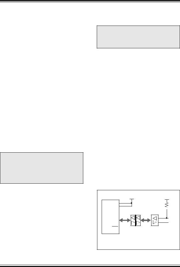
17.2.2.2External Transceiver
This module provides support for use with an off-chip transceiver. The off-chip transceiver is intended for applications where physical conditions dictate the location of the transceiver to be away from the SIE. For example, applications that require isolation from the USB could use an external transceiver through some isolation to the microcontroller’s SIE (Figure 17-2). External transceiver operation is enabled by setting the UTRDIS bit.
FIGURE 17-2: TYPICAL EXTERNAL TRANSCEIVER WITH ISOLATION
PIC® |
VDD Isolated |
3.3V Derived |
|
Microcontroller |
from USB |
from USB |
|
|
|||
|
VDD |
|
|
|
VUSB |
|
1.5 kΩ |
|
VM |
Isolation |
|
|
Transceiver |
||
|
VP |
||
|
|
D+ |
|
|
RCV |
|
|
|
VMO |
|
D- |
|
VPO |
|
|
|
|
|
|
|
UOE |
|
|
Note: |
The above setting shows a simplified schematic |
||
|
for a full-speed configuration using an external |
||
|
transceiver with isolation. |
|
|
♥ 2007 Microchip Technology Inc.
Preliminary
DS39632D-page 165

PIC18F2455/2550/4455/4550
REGISTER 17-2: UCFG: USB CONFIGURATION REGISTER
R/W-0 |
|
|
R/W-0 |
|
U-0 |
R/W-0 |
R/W-0 |
R/W-0 |
R/W-0 |
R/W-0 |
|||||
|
|
|
|
|
|
|
|
|
|
|
|
||||
UTEYE |
UOEMON(1) |
|
— |
|
UPUEN(2,3) |
UTRDIS(2) |
FSEN(2) |
PPB1 |
PPB0 |
||||||
bit 7 |
|
|
|
|
|
|
|
|
|
|
|
|
|
|
bit 0 |
|
|
|
|
|
|
|
|
|
|
|
|
|
|
|
|
|
|
|
|
|
|
|
|
|
|
|
|
|
|
|
|
Legend: |
|
|
|
|
|
|
|
|
|
|
|
|
|
|
|
R = Readable bit |
|
|
|
|
|
W = Writable bit |
U = Unimplemented bit, read as ‘0’ |
|
|||||||
-n = Value at POR |
|
|
|
|
‘1’ = Bit is set |
|
‘0’ = Bit is cleared |
x = Bit is unknown |
|||||||
|
|
|
|
|
|
||||||||||
bit 7 |
UTEYE: USB Eye Pattern Test Enable bit |
|
|
|
|
||||||||||
|
1 |
= |
|
Eye pattern test enabled |
|
|
|
|
|
||||||
|
0 |
= |
|
Eye pattern test disabled |
|
|
|
|
|
||||||
bit 6 |
UOEMON: USB |
|
Monitor Enable bit(1) |
|
|
|
|
||||||||
OE |
|
|
|
|
|||||||||||
|
1 |
= |
|
UOE |
signal active; it indicates intervals during which the D+/D- lines are driving |
|
|||||||||
|
0 |
= |
|
UOE signal inactive |
|
|
|
|
|
||||||
bit 5 |
Unimplemented: Read as ‘0’ |
|
|
|
|
||||||||||
bit 4 |
UPUEN: USB On-Chip Pull-up Enable bit(2,3) |
|
|
|
|||||||||||
|
1 |
= On-chip pull-up enabled (pull-up on D+ with FSEN = 1 or D- with FSEN = 0) |
|
||||||||||||
|
0 |
= On-chip pull-up disabled |
|
|
|
|
|
||||||||
bit 3 |
UTRDIS: On-Chip Transceiver Disable bit(2) |
|
|
|
|||||||||||
|
1 |
= On-chip transceiver disabled; digital transceiver interface enabled |
|
|
|||||||||||
|
0 |
= On-chip transceiver active |
|
|
|
|
|||||||||
bit 2 |
FSEN: Full-Speed Enable bit(2) |
|
|
|
|
||||||||||
|
1 |
= Full-speed device: controls transceiver edge rates; requires input clock at 48 MHz |
|
||||||||||||
|
0 |
= Low-speed device: controls transceiver edge rates; requires input clock at 6 MHz |
|
||||||||||||
bit 1-0 |
PPB1:PPB0: Ping-Pong Buffers Configuration bits |
|
|
|
|||||||||||
11 = Even/Odd ping-pong buffers enabled for Endpoints 1 to 15 10 = Even/Odd ping-pong buffers enabled for all endpoints
01 = Even/Odd ping-pong buffer enabled for OUT Endpoint 0 00 = Even/Odd ping-pong buffers disabled
Note 1: If UTRDIS is set, the UOE signal will be active independent of the UOEMON bit setting.
2:The UPUEN, UTRDIS and FSEN bits should never be changed while the USB module is enabled. These values must be preconfigured prior to enabling the module.
3:This bit is only valid when the on-chip transceiver is active (UTRDIS = 0); otherwise, it is ignored.
There are 6 signals from the module to communicate with and control an external transceiver:
•VM: Input from the single-ended D- line
•VP: Input from the single-ended D+ line
•RCV: Input from the differential receiver
•VMO: Output to the differential line driver
•VPO: Output to the differential line driver
•UOE: Output enable
The VPO and VMO signals are outputs from the SIE to the external transceiver. The RCV signal is the output from the external transceiver to the SIE; it represents the differential signals from the serial bus translated into a single pulse train. The VM and VP signals are used to report conditions on the serial bus to the SIE that can’t be captured with the RCV signal. The combinations of states of these signals and their interpretation are listed in Table 17-1 and Table 17-2.
DS39632D-page 166 |
Preliminary |
♥ 2007 Microchip Technology Inc. |
PIC18F2455/2550/4455/4550
TABLE 17-1: DIFFERENTIAL OUTPUTS TO
TRANSCEIVER
VPO |
VMO |
Bus State |
|
|
|
|
|
|
0 |
0 |
Single-Ended Zero |
|
|
|
0 |
1 |
Differential ‘0’ |
|
|
|
1 |
0 |
Differential ‘1’ |
|
|
|
1 |
1 |
Illegal Condition |
|
|
|
TABLE 17-2: SINGLE-ENDED INPUTS
|
|
|
|
FROM TRANSCEIVER |
VP |
|
VM |
Bus State |
|
|
|
|
|
|
|
|
|
|
|
0 |
0 |
Single-Ended Zero |
||
|
|
|
|
|
0 |
1 |
Low Speed |
||
|
|
|
|
|
1 |
0 |
High Speed |
||
|
|
|
|
|
1 |
1 |
Error |
||
|
|
|
|
|
|
|
|
|
|
The UOE signal toggles the state of the external transceiver. This line is pulled low by the device to enable the transmission of data from the SIE to an external device.
17.2.2.3Internal Pull-up Resistors
The PIC18FX455/X550 devices have built-in pull-up resistors designed to meet the requirements for low-speed and full-speed USB. The UPUEN bit (UCFG<4>) enables the internal pull-ups. Figure 17-1 shows the pull-ups and their control.
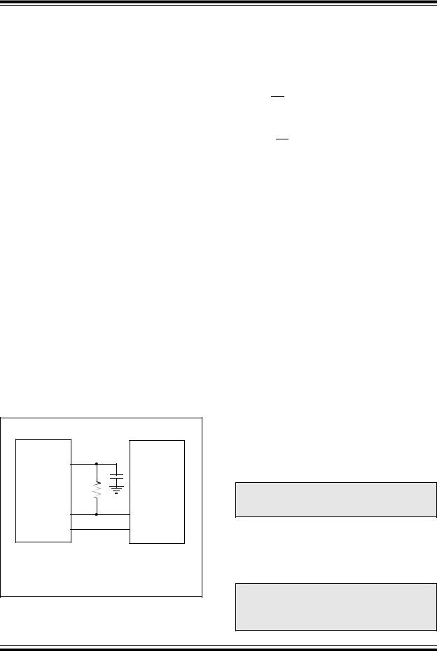
17.2.2.4External Pull-up Resistors
External pull-up may also be used. The VUSB pin may be used to pull up D+ or D-. The pull-up resistor must be 1.5 kΩ (±5%) as required by the USB specifications. Figure 17-3 shows an example.
FIGURE 17-3: EXTERNAL CIRCUITRY
PIC® |
Host |
Microcontroller |
Controller/HUB |
VUSB |
1.5 kΩ |
D+ |
D- |
Note: The above setting shows a typical connection for a full-speed configuration using an on-chip regulator and an external pull-up resistor.
17.2.2.5Ping-Pong Buffer Configuration
The usage of ping-pong buffers is configured using the PPB1:PPB0 bits. Refer to Section 17.4.4 “Ping-Pong Buffering” for a complete explanation of the ping-pong buffers.
17.2.2.6USB Output Enable Monitor
The USB OE monitor provides indication as to whether the SIE is listening to the bus or actively driving the bus. This is enabled by default when using an external transceiver or when UCFG<6> = 1.
The USB OE monitoring is useful for initial system debugging, as well as scope triggering during eye pattern generation tests.
17.2.2.7Eye Pattern Test Enable
An automatic eye pattern test can be generated by the module when the UCFG<7> bit is set. The eye pattern output will be observable based on module settings, meaning that the user is first responsible for configuring the SIE clock settings, pull-up resistor and Transceiver mode. In addition, the module has to be enabled.
Once UTEYE is set, the module emulates a switch from a receive to transmit state and will start transmitting a J-K-J-K bit sequence (K-J-K-J for full speed). The sequence will be repeated indefinitely while the Eye Pattern Test mode is enabled.
Note that this bit should never be set while the module is connected to an actual USB system. This test mode is intended for board verification to aid with USB certification tests. It is intended to show a system developer the noise integrity of the USB signals which can be affected by board traces, impedance mismatches and proximity to other system components. It does not properly test the transition from a receive to a transmit state. Although the eye pattern is not meant to replace the more complex USB certification test, it should aid during first order system debugging.
17.2.2.8Internal Regulator
The PIC18FX455/X550 devices have a built-in 3.3V regulator to provide power to the internal transceiver and provide a source for the internal/external pull-ups. An external 220 nF (±20%) capacitor is required for stability.
Note: The drive from VUSB is sufficient to only drive an external pull-up in addition to the internal transceiver.
The regulator is enabled by default and can be disabled through the VREGEN Configuration bit. When enabled, the voltage is visible on pin VUSB. When the regulator is disabled, a 3.3V source must be provided through the VUSB pin for the internal transceiver. If the internal transceiver is disabled, VUSB is not used.
Note 1: Do not enable the internal regulator if an external regulator is connected to VUSB.
2:VDD must be greater than VUSB at all times, even with the regulator disabled.
♥ 2007 Microchip Technology Inc. |
Preliminary |
DS39632D-page 167