

- •Universal Serial Bus Features:
- •Power-Managed Modes:
- •Flexible Oscillator Structure:
- •Peripheral Highlights:
- •Special Microcontroller Features:
- •Pin Diagrams
- •Pin Diagrams (Continued)
- •Table of Contents
- •Most Current Data Sheet
- •Errata
- •Customer Notification System
- •1.0 Device Overview
- •1.1 New Core Features
- •1.1.1 nanoWatt Technology
- •1.1.2 Universal Serial Bus (USB)
- •1.1.3 Multiple Oscillator Options and Features
- •1.2 Other Special Features
- •1.3 Details on Individual Family Members
- •FIGURE 1-2: PIC18F4455/4550 (40/44-Pin) Block Diagram
- •2.0 Oscillator Configurations
- •2.1 Overview
- •2.1.1 Oscillator Control
- •2.2 Oscillator Types
- •2.2.1 Oscillator Modes and USB Operation
- •2.2.2 Crystal Oscillator/Ceramic Resonators
- •FIGURE 2-2: Crystal/Ceramic Resonator Operation (XT, HS or HSPLL Configuration)
- •TABLE 2-1: Capacitor Selection for Ceramic Resonators
- •TABLE 2-2: Capacitor Selection for Crystal Oscillator
- •FIGURE 2-3: External Clock Input Operation (HS Osc Configuration)
- •2.2.3 External Clock Input
- •FIGURE 2-5: External Clock Input Operation (ECIO and ECPIO Configuration)
- •2.2.4 PLL Frequency Multiplier
- •FIGURE 2-6: PLL Block Diagram (HS Mode)
- •2.2.5 Internal Oscillator Block
- •2.3 Oscillator Settings for USB
- •2.3.2 Running Different USB and Microcontroller Clocks
- •2.4 Clock Sources and Oscillator Switching
- •2.4.1 Oscillator Control Register
- •2.4.2 Oscillator Transitions
- •3.0 Power-Managed Modes
- •3.1.1 Clock Sources
- •TABLE 3-1: Power-Managed Modes
- •3.1.3 Clock Transitions and Status Indicators
- •3.1.4 Multiple Sleep Commands
- •3.2 Run Modes
- •3.2.1 PRI_RUN Mode
- •3.2.2 SEC_RUN Mode
- •FIGURE 3-1: Transition Timing for Entry to SEC_RUN Mode
- •FIGURE 3-2: Transition Timing From SEC_RUN Mode to PRI_RUN Mode (HSPLL)
- •3.2.3 RC_RUN Mode
- •FIGURE 3-4: Transition Timing From RC_RUN Mode to PRI_RUN Mode
- •3.3 Sleep Mode
- •3.4 Idle Modes
- •FIGURE 3-5: Transition Timing for Entry to Sleep Mode
- •FIGURE 3-6: Transition Timing for Wake From Sleep (HSPLL)
- •3.4.1 PRI_IDLE Mode
- •3.4.2 SEC_IDLE Mode
- •FIGURE 3-7: Transition Timing for Entry to Idle Mode
- •FIGURE 3-8: Transition Timing for Wake From Idle to Run Mode
- •3.4.3 RC_IDLE Mode
- •3.5 Exiting Idle and Sleep Modes
- •3.5.1 Exit By Interrupt
- •3.5.3 Exit By Reset
- •TABLE 3-2: Exit Delay on Wake-up By Reset From Sleep Mode or Any Idle Mode (By Clock Sources)
- •4.0 Reset
- •4.1 RCON Register
- •FIGURE 4-1: Simplified Block Diagram of On-Chip Reset Circuit
- •4.2 Master Clear Reset (MCLR)
- •FIGURE 4-2: External Power-on Reset Circuit (for Slow Vdd Power-up)
- •4.4.1 Software Enabled BOR
- •4.4.2 Detecting BOR
- •4.4.3 Disabling BOR in Sleep Mode
- •TABLE 4-1: BOR Configurations
- •4.5 Device Reset Timers
- •FIGURE 4-3: Time-out Sequence on Power-up (MCLR Tied to Vdd, Vdd Rise < Tpwrt)
- •FIGURE 4-4: Time-out Sequence on Power-up (MCLR Not Tied to Vdd): Case 1
- •FIGURE 4-5: Time-out Sequence on Power-up (MCLR Not Tied to Vdd): Case 2
- •FIGURE 4-6: Slow Rise Time (MCLR Tied to Vdd, Vdd Rise > Tpwrt)
- •FIGURE 4-7: Time-out Sequence on POR w/PLL Enabled (MCLR Tied to Vdd)
- •4.6 Reset State of Registers
- •5.0 Memory Organization
- •5.1 Program Memory Organization
- •FIGURE 5-1: Program Memory Map and Stack for PIC18F2455/2550/4455/4550 Devices
- •5.1.1 Program Counter
- •5.1.2 Return Address Stack
- •FIGURE 5-2: Return Address Stack and Associated Registers
- •5.1.3 Fast Register Stack
- •5.2 PIC18 Instruction Cycle
- •5.2.1 Clocking Scheme
- •5.2.2 Instruction Flow/Pipelining
- •5.2.3 Instructions in Program Memory
- •EXAMPLE 5-4: Two-Word Instructions
- •5.3 Data Memory Organization
- •5.3.2 Bank Select Register (BSR)
- •FIGURE 5-5: Data Memory Map for PIC18F2455/2550/4455/4550 Devices
- •FIGURE 5-6: Use of the Bank Select Register (Direct Addressing)
- •5.3.3 Access Bank
- •5.3.4 General Purpose Register File
- •5.3.5 Special Function Registers
- •5.3.6 Status Register
- •5.4 Data Addressing Modes
- •5.4.1 Inherent and Literal Addressing
- •5.4.2 Direct Addressing
- •5.4.3 Indirect Addressing
- •FIGURE 5-7: Indirect Addressing
- •5.5 Program Memory and the Extended Instruction Set
- •5.6 Data Memory and the Extended Instruction Set
- •5.6.1 Indexed Addressing with Literal Offset
- •5.6.2 Instructions Affected By Indexed Literal Offset Mode
- •5.6.3 Mapping the Access Bank in Indexed Literal Offset Mode
- •5.6.4 BSR in Indexed Literal Offset Mode
- •FIGURE 5-9: Remapping the Access Bank with Indexed Literal Offset Addressing
- •6.0 Flash Program Memory
- •6.1 Table Reads and Table Writes
- •FIGURE 6-2: Table Write Operation
- •6.2 Control Registers
- •6.2.1 EECON1 and EECON2 Registers
- •6.2.2 Table Latch Register (TABLAT)
- •6.2.3 Table Pointer Register (TBLPTR)
- •6.2.4 Table Pointer Boundaries
- •FIGURE 6-3: Table Pointer Boundaries Based on Operation
- •6.3 Reading the Flash Program Memory
- •FIGURE 6-4: Reads From Flash Program Memory
- •6.4 Erasing Flash Program Memory
- •6.4.1 Flash Program Memory Erase Sequence
- •6.5 Writing to Flash Program Memory
- •FIGURE 6-5: Table Writes to Flash Program Memory
- •6.5.1 Flash Program Memory Write Sequence
- •EXAMPLE 6-3: Writing to Flash Program Memory (Continued)
- •6.5.2 Write Verify
- •6.5.3 Unexpected Termination of Write Operation
- •6.5.4 Protection Against Spurious Writes
- •6.6 Flash Program Operation During Code Protection
- •7.0 Data EEPROM Memory
- •7.1 EECON1 and EECON2 Registers
- •7.2 Reading the Data EEPROM Memory
- •7.3 Writing to the Data EEPROM Memory
- •7.4 Write Verify
- •EXAMPLE 7-1: Data EEPROM Read
- •7.6 Protection Against Spurious Write
- •7.7 Using the Data EEPROM
- •TABLE 7-1: Registers Associated with Data EEPROM Memory
- •8.0 8 x 8 Hardware Multiplier
- •8.1 Introduction
- •8.2 Operation
- •EQUATION 8-1: 16 x 16 Unsigned Multiplication Algorithm
- •EQUATION 8-2: 16 x 16 Signed Multiplication Algorithm
- •9.0 Interrupts
- •9.1 USB Interrupts
- •FIGURE 9-1: Interrupt Logic
- •9.2 INTCON Registers
- •9.3 PIR Registers
- •9.4 PIE Registers
- •9.5 IPR Registers
- •9.6 RCON Register
- •9.7 INTn Pin Interrupts
- •9.8 TMR0 Interrupt
- •9.10 Context Saving During Interrupts
- •10.0 I/O Ports
- •FIGURE 10-1: Generic I/O Port Operation
- •10.1 PORTA, TRISA and LATA Registers
- •EXAMPLE 10-1: Initializing PORTA
- •10.2 PORTB, TRISB and LATB Registers
- •EXAMPLE 10-2: Initializing PORTB
- •10.3 PORTC, TRISC and LATC Registers
- •TABLE 10-6: Summary of Registers Associated with PORTC
- •10.4 PORTD, TRISD and LATD Registers
- •10.5 PORTE, TRISE and LATE Registers
- •TABLE 10-9: PORTE I/O Summary
- •TABLE 10-10: Summary of Registers Associated with PORTE
- •11.0 Timer0 Module
- •11.1 Timer0 Operation
- •11.3 Prescaler
- •11.3.1 Switching Prescaler Assignment
- •11.4 Timer0 Interrupt
- •TABLE 11-1: Registers Associated with Timer0
- •12.0 Timer1 Module
- •12.1 Timer1 Operation
- •FIGURE 12-2: Timer1 Block Diagram (16-bit Read/Write Mode)
- •12.3 Timer1 Oscillator
- •12.3.1 Using Timer1 as a Clock Source
- •12.3.3 Timer1 Oscillator Layout Considerations
- •FIGURE 12-4: Oscillator Circuit with Grounded Guard Ring
- •12.4 Timer1 Interrupt
- •12.5 Resetting Timer1 Using the CCP Special Event Trigger
- •TABLE 12-2: Registers Associated with Timer1 as a Timer/Counter
- •13.0 Timer2 Module
- •13.1 Timer2 Operation
- •13.2 Timer2 Interrupt
- •13.3 TMR2 Output
- •TABLE 13-1: Registers Associated with Timer2 as a Timer/Counter
- •14.0 Timer3 Module
- •14.1 Timer3 Operation
- •14.3 Using the Timer1 Oscillator as the Timer3 Clock Source
- •14.4 Timer3 Interrupt
- •14.5 Resetting Timer3 Using the CCP Special Event Trigger
- •TABLE 14-1: Registers Associated with Timer3 as a Timer/Counter
- •15.0 Capture/Compare/PWM (CCP) Modules
- •Register 15-1: CCPxCON: Standard CCPx Control Register
- •15.1 CCP Module Configuration
- •15.1.1 CCP Modules and Timer Resources
- •TABLE 15-1: CCP Mode – Timer Resource
- •15.1.2 CCP2 Pin Assignment
- •TABLE 15-2: Interactions Between CCP1 and CCP2 for Timer Resources
- •15.2 Capture Mode
- •15.2.1 CCP Pin Configuration
- •15.2.2 Timer1/Timer3 Mode Selection
- •15.2.3 Software Interrupt
- •15.2.4 CCP Prescaler
- •EXAMPLE 15-1: Changing Between Capture Prescalers (CCP2 Shown)
- •FIGURE 15-1: Capture Mode Operation Block Diagram
- •15.3 Compare Mode
- •15.3.1 CCP Pin Configuration
- •15.3.2 Timer1/Timer3 Mode Selection
- •15.3.3 Software Interrupt Mode
- •15.3.4 Special Event Trigger
- •FIGURE 15-2: Compare Mode Operation Block Diagram
- •TABLE 15-3: Registers Associated with Capture, Compare, Timer1 and Timer3
- •15.4 PWM Mode
- •FIGURE 15-3: Simplified PWM Block Diagram
- •15.4.1 PWM Period
- •EQUATION 15-1:
- •15.4.2 PWM Duty Cycle
- •EQUATION 15-2:
- •EQUATION 15-3:
- •TABLE 15-4: Example PWM Frequencies and Resolutions at 40 MHz
- •15.4.4 Setup for PWM Operation
- •16.0 Enhanced Capture/Compare/PWM (ECCP) Module
- •Register 16-1: CCP1CON: ECCP Control Register (40/44-Pin Devices)
- •16.1 ECCP Outputs and Configuration
- •16.1.1 ECCP Modules and Timer Resources
- •16.2 Capture and Compare Modes
- •16.2.1 Special Event Trigger
- •16.3 Standard PWM Mode
- •TABLE 16-1: Pin Assignments for Various ECCP1 Modes
- •16.4 Enhanced PWM Mode
- •16.4.1 PWM Period
- •EQUATION 16-1:
- •FIGURE 16-1: Simplified Block Diagram of the Enhanced PWM Module
- •16.4.2 PWM Duty Cycle
- •EQUATION 16-2:
- •EQUATION 16-3:
- •16.4.3 PWM Output Configurations
- •TABLE 16-2: Example PWM Frequencies and Resolutions at 40 MHz
- •FIGURE 16-2: PWM Output Relationships (Active-High State)
- •FIGURE 16-3: PWM Output Relationships (Active-Low State)
- •FIGURE 16-4: Half-Bridge PWM Output
- •FIGURE 16-5: Examples of Half-Bridge Output Mode Applications
- •FIGURE 16-6: Full-Bridge PWM Output
- •FIGURE 16-7: Example of Full-Bridge Application
- •FIGURE 16-9: PWM Direction Change at Near 100% Duty Cycle
- •Register 16-2: ECCP1DEL: PWM Dead-Band Delay Register
- •Register 16-3: ECCP1AS: Enhanced Capture/Compare/PWM Auto-Shutdown Control Register
- •FIGURE 16-10: PWM Auto-Shutdown (PRSEN = 1, Auto-Restart Enabled)
- •FIGURE 16-11: PWM Auto-Shutdown (PRSEN = 0, Auto-Restart Disabled)
- •16.4.9 Setup for PWM Operation
- •16.4.11 Effects of a Reset
- •TABLE 16-3: Registers Associated with ECCP Module And Timer1 to Timer3
- •17.0 Universal Serial Bus (USB)
- •17.1 Overview of the USB Peripheral
- •17.2 USB Status and Control
- •17.2.1 USB Control Register (UCON)
- •Register 17-1: UCON: USB Control Register
- •17.2.2 USB Configuration Register (UCFG)
- •FIGURE 17-2: Typical External Transceiver with Isolation
- •Register 17-2: UCFG: USB Configuration Register
- •FIGURE 17-3: External Circuitry
- •17.2.3 USB Status Register (USTAT)
- •Register 17-3: USTAT: USB Status Register
- •17.2.4 USB Endpoint Control
- •Register 17-4: UEPn: USB Endpoint n Control Register (UEP0 Through UEP15)
- •17.2.5 USB Address Register (UADDR)
- •17.2.6 USB Frame Number Registers (UFRMH:UFRML)
- •FIGURE 17-5: Implementation of USB RAM in Data Memory Space
- •17.4 Buffer Descriptors and the Buffer Descriptor Table
- •17.4.1 BD Status and Configuration
- •FIGURE 17-6: Example of a Buffer Descriptor
- •TABLE 17-3: Effect of DTSEN Bit on Odd/Even (DATA0/DATA1) Packet Reception
- •17.4.2 BD Byte Count
- •17.4.3 BD Address Validation
- •FIGURE 17-7: Buffer Descriptor Table Mapping for Buffering Modes
- •TABLE 17-4: Assignment of Buffer Descriptors for the Different Buffering Modes
- •TABLE 17-5: Summary of USB Buffer Descriptor Table Registers
- •17.5 USB Interrupts
- •17.5.1 USB Interrupt Status Register (UIR)
- •Register 17-7: UIR: USB Interrupt Status Register
- •EXAMPLE 17-1: Clearing ACTVIF Bit (UIR<2>)
- •17.5.2 USB Interrupt Enable Register (UIE)
- •Register 17-8: UIE: USB Interrupt Enable Register
- •17.5.3 USB Error Interrupt Status Register (UEIR)
- •Register 17-9: UEIR: USB Error Interrupt Status Register
- •17.5.4 USB Error Interrupt Enable Register (UEIE)
- •Register 17-10: UEIE: USB Error Interrupt Enable Register
- •17.6 USB Power Modes
- •17.6.1 Bus Power Only
- •FIGURE 17-10: Bus Power Only
- •FIGURE 17-11: Self-power Only
- •FIGURE 17-12: Dual Power Example
- •17.7 Streaming Parallel Port
- •17.8 Oscillator
- •17.9 USB Firmware and Drivers
- •TABLE 17-6: Registers Associated with USB Module Operation(1)
- •17.10 Overview of USB
- •17.10.1 Layered Framework
- •17.10.2 Frames
- •17.10.3 Transfers
- •17.10.4 Power
- •FIGURE 17-13: USB Layers
- •17.10.5 Enumeration
- •17.10.6 Descriptors
- •17.10.7 Bus Speed
- •17.10.8 Class Specifications and Drivers
- •18.0 Streaming Parallel Port
- •18.1 SPP Configuration
- •18.1.1 Enabling the SPP
- •Register 18-1: SPPCON: SPP Control Register
- •Register 18-2: SPPCFG: SPP Configuration Register
- •18.1.2 Clocking Data
- •18.1.3 Wait States
- •FIGURE 18-2: Timing for Microcontroller Write Address, Write Data and Read Data (No Wait States)
- •FIGURE 18-3: Timing for USB Write Address and Data (4 Wait States)
- •FIGURE 18-4: Timing for USB Write Address and Read Data (4 Wait States)
- •18.2 Setup for USB Control
- •18.3 Setup for Microcontroller Control
- •18.3.1 SPP Interrupts
- •18.3.2 Writing to the SPP
- •FIGURE 18-5: Transfer of Data Between USB SIE and SPP
- •18.3.3 Reading From the SPP
- •Register 18-3: SPPEPS: SPP Endpoint Address and Status Register
- •TABLE 18-1: Registers Associated with the Streaming Parallel Port
- •19.0 Master Synchronous Serial Port (MSSP) Module
- •19.1 Master SSP (MSSP) Module Overview
- •19.2 Control Registers
- •19.3 SPI Mode
- •19.3.1 Registers
- •Register 19-2: SSPCON1: MSSP Control Register 1 (SPI Mode)
- •19.3.2 Operation
- •19.3.3 Enabling SPI I/O
- •19.3.4 Typical Connection
- •19.3.5 Master Mode
- •FIGURE 19-3: SPI Mode Waveform (Master Mode)
- •19.3.6 Slave Mode
- •19.3.7 Slave Select Synchronization
- •FIGURE 19-4: Slave Synchronization Waveform
- •FIGURE 19-5: SPI Mode Waveform (Slave Mode with CKE = 0)
- •FIGURE 19-6: SPI Mode Waveform (Slave Mode with CKE = 1)
- •19.3.9 Effects of a Reset
- •19.3.10 Bus Mode Compatibility
- •TABLE 19-1: SPI Bus Modes
- •TABLE 19-2: Registers Associated with SPI Operation
- •FIGURE 19-7: MSSP Block Diagram (I2C™ Mode)
- •19.4.1 Registers
- •19.4.2 Operation
- •19.4.3 Slave Mode
- •EXAMPLE 19-2: Address Masking Examples
- •19.4.4 Clock Stretching
- •FIGURE 19-14: Clock Synchronization Timing
- •19.4.5 General Call Address Support
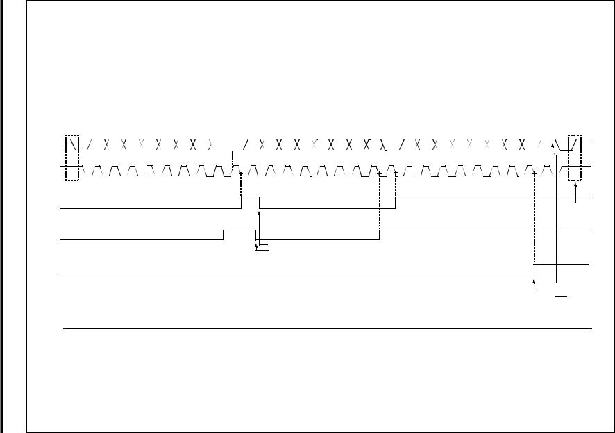
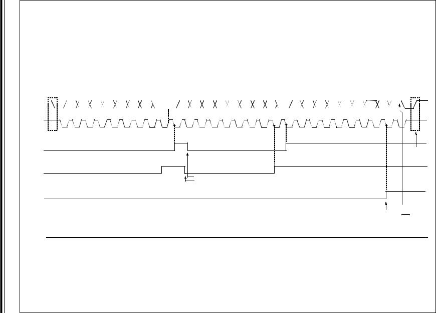
- •FIGURE 19-17: Slave Mode General Call Address Sequence (7 or 10-Bit Address Mode)
- •19.4.6 Master Mode
- •FIGURE 19-18: MSSP Block Diagram (I2C™ Master Mode)
- •19.4.7 Baud Rate
- •FIGURE 19-19: Baud Rate Generator Block Diagram
- •TABLE 19-3: I2C™ Clock Rate w/BRG
- •FIGURE 19-20: Baud Rate Generator Timing with Clock Arbitration
- •FIGURE 19-21: First Start Bit Timing
- •FIGURE 19-22: Repeated Start Condition Waveform
- •19.4.12 Acknowledge Sequence Timing
- •19.4.13 Stop Condition Timing
- •FIGURE 19-25: Acknowledge Sequence Waveform
- •FIGURE 19-26: Stop Condition Receive or Transmit Mode
- •19.4.14 Sleep Operation
- •19.4.15 EffectS of a Reset
- •FIGURE 19-27: Bus Collision Timing for Transmit and Acknowledge
- •FIGURE 19-28: Bus Collision During Start Condition (SDA Only)
- •FIGURE 19-29: Bus Collision During Start Condition (SCL = 0)
- •FIGURE 19-30: BRG Reset Due to SDA Arbitration During Start Condition
- •FIGURE 19-31: Bus Collision During a Repeated Start Condition (Case 1)
- •FIGURE 19-32: Bus Collision During Repeated Start Condition (Case 2)
- •FIGURE 19-33: Bus Collision During a Stop Condition (Case 1)
- •FIGURE 19-34: Bus Collision During a Stop Condition (Case 2)
- •TABLE 19-4: Registers Associated with I2C™ Operation
- •20.0 Enhanced Universal Synchronous Asynchronous Receiver Transmitter (EUSART)
- •20.1 Baud Rate Generator (BRG)
- •20.1.2 Sampling
- •TABLE 20-1: Baud Rate Formulas
- •EXAMPLE 20-1: Calculating Baud Rate Error
- •TABLE 20-2: Registers Associated with Baud Rate Generator
- •FIGURE 20-1: Automatic Baud Rate Calculation
- •FIGURE 20-2: BRG Overflow Sequence
- •20.2 EUSART Asynchronous Mode
- •20.2.1 EUSART Asynchronous Transmitter
- •FIGURE 20-3: EUSART Transmit Block Diagram
- •FIGURE 20-4: Asynchronous Transmission, TXCKP = 0 (TX Not Inverted)
- •TABLE 20-5: Registers Associated with Asynchronous Transmission
- •20.2.2 EUSART Asynchronous Receiver
- •FIGURE 20-6: EUSART Receive Block Diagram
- •FIGURE 20-7: Asynchronous Reception, RXDTP = 0 (RX Not Inverted)
- •FIGURE 20-8: Auto-Wake-up Bit (WUE) Timings During Normal Operation
- •20.2.5 Break Character Sequence
- •20.2.6 Receiving A Break Character
- •FIGURE 20-10: Send Break Character Sequence
- •20.3 EUSART Synchronous Master Mode
- •20.3.1 EUSART Synchronous Master Transmission
- •FIGURE 20-11: Synchronous Transmission
- •FIGURE 20-12: Synchronous Transmission (Through TXEN)
- •20.3.2 EUSART Synchronous Master Reception
- •FIGURE 20-13: Synchronous Reception (Master Mode, SREN)
- •TABLE 20-8: Registers Associated with Synchronous Master Reception
- •20.4 EUSART Synchronous Slave Mode
- •20.4.1 EUSART Synchronous Slave Transmission
- •TABLE 20-9: Registers Associated with Synchronous Slave Transmission
- •20.4.2 EUSART Synchronous Slave Reception
- •TABLE 20-10: Registers Associated with Synchronous Slave Reception
- •21.1 A/D Acquisition Requirements
- •EQUATION 21-1: Acquisition Time
- •EQUATION 21-2: A/D Minimum Charging Time
- •EQUATION 21-3: Calculating the Minimum Required Acquisition Time
- •21.2 Selecting and Configuring Acquisition Time
- •21.3 Selecting the A/D Conversion Clock
- •TABLE 21-1: Tad vs. Device Operating Frequencies
- •21.5 Configuring Analog Port Pins
- •21.6 A/D Conversions
- •21.7 Discharge
- •FIGURE 21-4: A/D Conversion Tad Cycles (ACQT<2:0> = 000, Tacq = 0)
- •21.8 Use of the CCP2 Trigger
- •TABLE 21-2: Registers Associated with A/D Operation
- •22.0 Comparator Module
- •22.1 Comparator Configuration
- •22.2 Comparator Operation
- •22.3 Comparator Reference
- •FIGURE 22-2: Single Comparator
- •22.3.1 External Reference Signal
- •22.3.2 Internal Reference Signal
- •22.4 Comparator Response Time
- •22.5 Comparator Outputs
- •FIGURE 22-3: Comparator Output Block Diagram
- •22.6 Comparator Interrupts
- •22.7 Comparator Operation During Sleep
- •22.8 Effects of a Reset
- •22.9 Analog Input Connection Considerations
- •TABLE 22-1: Registers Associated with Comparator Module
- •23.0 Comparator Voltage Reference Module
- •23.1 Configuring the Comparator Voltage Reference
- •FIGURE 23-1: Comparator Voltage Reference Block Diagram
- •23.2 Voltage Reference Accuracy/Error
- •23.3 Operation During Sleep
- •23.4 Effects of a Reset
- •23.5 Connection Considerations
- •FIGURE 23-2: Comparator Voltage Reference Output Buffer Example
- •24.1 Operation
- •FIGURE 24-1: HLVD Module Block Diagram (with External Input)
- •24.2 HLVD Setup
- •24.3 Current Consumption
- •FIGURE 24-2: Low-Voltage Detect Operation (VDIRMAG = 0)
- •FIGURE 24-3: High-Voltage Detect Operation (VDIRMAG = 1)
- •24.5 Applications
- •24.6 Operation During Sleep
- •24.7 Effects of a Reset
- •TABLE 24-1: Registers Associated with High/Low-Voltage Detect Module
- •25.0 Special Features of the CPU
- •25.1 Configuration Bits
- •TABLE 25-1: Configuration Bits and Device IDs
- •Register 25-5: CONFIG3H: Configuration Register 3 High (Byte Address 300005h)
- •Register 25-6: CONFIG4L: Configuration Register 4 Low (Byte Address 300006h)
- •Register 25-7: CONFIG5L: Configuration Register 5 Low (Byte Address 300008h)
- •Register 25-8: CONFIG5H: Configuration Register 5 High (Byte Address 300009h)
- •Register 25-9: CONFIG6L: Configuration Register 6 Low (Byte Address 30000Ah)
- •Register 25-10: CONFIG6H: Configuration Register 6 High (Byte Address 30000Bh)
- •Register 25-11: CONFIG7L: Configuration Register 7 Low (Byte Address 30000Ch)
- •Register 25-12: CONFIG7H: Configuration Register 7 High (Byte Address 30000Dh)
- •Register 25-13: DEVID1: Device ID Register 1 for PIC18F2455/2550/4455/4550 Devices
- •Register 25-14: DEVID2: Device ID Register 2 for PIC18F2455/2550/4455/4550 Devices
- •25.2 Watchdog Timer (WDT)
- •25.2.1 Control Register
- •FIGURE 25-1: WDT Block Diagram
- •Register 25-15: WDTCON: Watchdog Timer Control Register
- •TABLE 25-2: Summary of Watchdog Timer Registers
- •25.3 Two-Speed Start-up
- •FIGURE 25-2: Timing Transition for Two-Speed Start-up (INTOSC to HSPLL)
- •FIGURE 25-3: FSCM Block Diagram
- •25.4.1 FSCM and the Watchdog Timer
- •FIGURE 25-4: FSCM Timing Diagram
- •25.5 Program Verification and Code Protection
- •TABLE 25-3: Summary of Code Protection Registers
- •25.5.1 Program Memory Code Protection
- •FIGURE 25-7: External Block Table Read (EBTRn) Disallowed
- •FIGURE 25-8: External Block Table Read (EBTRn) Allowed
- •25.5.2 Data EEPROM Code Protection
- •25.5.3 Configuration Register Protection
- •25.6 ID Locations
- •TABLE 25-4: Debugger Resources
- •25.9 Special ICPORT Features (Designated Packages Only)
- •25.9.1 Dedicated ICD/ICSP Port
- •TABLE 25-5: Equivalent Pins for Legacy and Dedicated ICD/ICSP™ Ports
- •25.10 Single-Supply ICSP Programming
- •26.0 Instruction Set Summary
- •26.1 Standard Instruction Set
- •TABLE 26-1: Opcode Field Descriptions
- •FIGURE 26-1: General Format for Instructions
- •26.1.1 Standard Instruction Set
- •26.2 Extended Instruction Set
- •26.2.1 Extended Instruction Syntax
- •TABLE 26-3: Extensions to the PIC18 Instruction Set
- •26.2.2 Extended Instruction Set
- •26.2.4 Considerations When Enabling the Extended Instruction Set
- •27.0 Development Support
- •27.1 MPLAB Integrated Development Environment Software
- •27.2 MPASM Assembler
- •27.3 MPLAB C18 and MPLAB C30 C Compilers
- •27.4 MPLINK Object Linker/ MPLIB Object Librarian
- •27.5 MPLAB ASM30 Assembler, Linker and Librarian
- •27.6 MPLAB SIM Software Simulator
- •27.10 MPLAB PM3 Device Programmer
- •27.11 PICSTART Plus Development Programmer
- •27.12 Demonstration, Development and Evaluation Boards
- •28.0 Electrical Characteristics
- •Absolute Maximum Ratings(†)
- •FIGURE 28-1: PIC18F2455/2550/4455/4550 Voltage-Frequency Graph (Industrial)
- •FIGURE 28-2: PIC18LF2455/2550/4455/4550 Voltage-Frequency Graph (Industrial)
- •TABLE 28-2: Comparator Specifications
- •TABLE 28-3: Voltage Reference Specifications
- •TABLE 28-4: USB Module Specifications
- •TABLE 28-5: USB Internal Voltage Regulator Specifications
- •FIGURE 28-3: High/Low-Voltage Detect Characteristics
- •TABLE 28-6: High/Low-Voltage Detect Characteristics
- •28.4 AC (Timing) Characteristics
- •28.4.1 Timing Parameter Symbology
- •28.4.2 Timing Conditions
- •TABLE 28-7: Temperature and Voltage Specifications – AC
- •FIGURE 28-4: Load Conditions for Device Timing Specifications
- •28.4.3 Timing Diagrams And Specifications
- •FIGURE 28-5: External Clock Timing (All Modes Except PLL)
- •TABLE 28-8: External Clock Timing Requirements
- •TABLE 28-9: PLL Clock Timing Specifications (Vdd = 3.0V to 5.5V)
- •FIGURE 28-6: CLKO and I/O Timing
- •TABLE 28-11: CLKO and I/O Timing Requirements
- •FIGURE 28-7: Reset, Watchdog Timer, Oscillator Start-up Timer and Power-up Timer Timing
- •FIGURE 28-9: Timer0 and Timer1 External Clock Timings
- •TABLE 28-13: Timer0 and Timer1 External Clock Requirements
- •FIGURE 28-10: Capture/Compare/PWM Timings (All CCP Modules)
- •TABLE 28-14: Capture/Compare/PWM Requirements (All CCP Modules)
- •FIGURE 28-15: I2C™ Bus Start/Stop Bits Timing
- •TABLE 28-19: I2C™ Bus Start/Stop Bits Requirements (Slave Mode)
- •FIGURE 28-16: I2C™ Bus Data Timing
- •TABLE 28-20: I2C™ Bus Data Requirements (Slave Mode)
- •FIGURE 28-17: Master SSP I2C™ Bus Start/Stop Bits Timing Waveforms
- •TABLE 28-21: Master SSP I2C™ Bus Start/Stop Bits Requirements
- •FIGURE 28-18: Master SSP I2C™ Bus Data Timing
- •TABLE 28-22: Master SSP I2C™ Bus Data Requirements
- •FIGURE 28-19: EUSART Synchronous Transmission (Master/Slave) Timing
- •TABLE 28-23: EUSART Synchronous Transmission Requirements
- •FIGURE 28-20: EUSART Synchronous Receive (Master/Slave) Timing
- •TABLE 28-24: EUSART Synchronous Receive Requirements
- •FIGURE 28-21: USB Signal Timing
- •TABLE 28-25: USB Low-Speed Timing Requirements
- •TABLE 28-26: USB Full-Speed Requirements
- •FIGURE 28-22: Streaming Parallel Port Timing (PIC18F4455/4550)
- •TABLE 28-27: Streaming Parallel Port Requirements (PIC18F4455/4550)
- •FIGURE 28-23: A/D Conversion Timing
- •TABLE 28-29: A/D Conversion Requirements
- •29.0 DC and AC Characteristics Graphs and Tables
- •30.0 Packaging Information
- •30.1 Package Marking Information
- •Package Marking Information (Continued)
- •30.2 Package Details
- •Appendix A: Revision History
- •Revision A (May 2004)
- •Revision B (October 2004)
- •Revision C (February 2006)
- •Revision D (January 2007)
- •Appendix B: Device Differences
- •Appendix C: Conversion Considerations
- •Appendix D: Migration From Baseline to Enhanced Devices
- •Appendix E: Migration From Mid-Range to Enhanced Devices
- •Appendix F: Migration From High-End to Enhanced Devices
- •INDEX
- •The Microchip Web Site
- •Customer Change Notification Service
- •Customer Support
- •Reader Response
- •PIC18F2455/2550/4455/4550 Product Identification System
- •Worldwide Sales and Service

PIC18F2455/2550/4455/4550
19.4.2OPERATION
The MSSP module functions are enabled by setting MSSP Enable bit, SSPEN (SSPCON1<5>).
The SSPCON1 register allows control of the I2C operation. Four mode selection bits (SSPCON1<3:0>) allow one of the following I2C modes to be selected:
•I2C Master mode, clock
•I2C Slave mode (7-bit address)
•I2C Slave mode (10-bit address)
•I2C Slave mode (7-bit address) with Start and Stop bit interrupts enabled
•I2C Slave mode (10-bit address) with Start and Stop bit interrupts enabled
•I2C Firmware Controlled Master mode, slave is Idle
Selection of any I2C mode with the SSPEN bit set forces the SCL and SDA pins to be open-drain, provided these pins are programmed as inputs by setting the appropriate TRISC or TRISD bits. To ensure proper operation of the module, pull-up resistors must be provided externally to the SCL and SDA pins.
19.4.3SLAVE MODE
In Slave mode, the SCL and SDA pins must be configured as inputs (TRISC<4:3> set). The MSSP module will override the input state with the output data when required (slave-transmitter).
The I2C Slave mode hardware will always generate an interrupt on an address match. Address masking will allow the hardware to generate an interrupt for more than one address (up to 31 in 7-bit addressing and up to 63 in 10-bit addressing). Through the mode select bits, the user can also choose to interrupt on Start and Stop bits.
When an address is matched, or the data transfer after an address match is received, the hardware automatically will generate the Acknowledge (ACK) pulse and load the SSPBUF register with the received value currently in the SSPSR register.
Any combination of the following conditions will cause the MSSP module not to give this ACK pulse:
•The Buffer Full bit, BF (SSPSTAT<0>), was set before the transfer was received.
•The overflow bit, SSPOV (SSPCON1<6>), was set before the transfer was received.
In this case, the SSPSR register value is not loaded into the SSPBUF, but bit SSPIF is set. The BF bit is cleared by reading the SSPBUF register, while bit SSPOV is cleared through software.
The SCL clock input must have a minimum high and low for proper operation. The high and low times of the I2C specification, as well as the requirement of the MSSP module, are shown in timing parameter 100 and parameter 101.
19.4.3.1Addressing
Once the MSSP module has been enabled, it waits for a Start condition to occur. Following the Start condition, the 8 bits are shifted into the SSPSR register. All incoming bits are sampled with the rising edge of the clock (SCL) line. The value of register SSPSR<7:1> is compared to the value of the SSPADD register. The address is compared on the falling edge of the eighth clock (SCL) pulse. If the addresses match and the BF and SSPOV bits are clear, the following events occur:
1.The SSPSR register value is loaded into the SSPBUF register.
2.The Buffer Full bit, BF, is set.
3.An ACK pulse is generated.
4.The MSSP Interrupt Flag bit, SSPIF, is set (and interrupt is generated, if enabled) on the falling edge of the ninth SCL pulse.
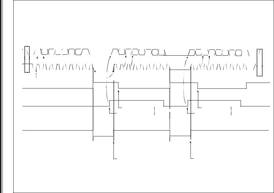
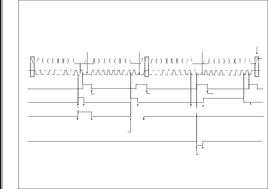
In 10-Bit Address mode, two address bytes need to be received by the slave. The five Most Significant bits (MSbs) of the first address byte specify if this is a 10-bit address. Bit R/W (SSPSTAT<2>) must specify a write so the slave device will receive the second address byte. For a 10-bit address, the first byte would equal ‘11110 A9 A8 0’, where ‘A9’ and ‘A8’ are the two MSbs of the address. The sequence of events for 10-bit address is as follows, with steps 7 through 9 for the slave-transmitter:
1.Receive first (high) byte of address (bits SSPIF, BF and UA (SSPSTAT<1>) are set on address match).
2.Update the SSPADD register with second (low) byte of address (clears bit UA and releases the SCL line).
3.Read the SSPBUF register (clears bit BF) and clear flag bit SSPIF.
4.Receive second (low) byte of address (bits SSPIF, BF and UA are set).
5.Update the SSPADD register with the first (high) byte of address. If match releases SCL line, this will clear bit UA.
6.Read the SSPBUF register (clears bit BF) and clear flag bit SSPIF.
7.Receive Repeated Start condition.
8.Receive first (high) byte of address (bits SSPIF and BF are set).
9.Read the SSPBUF register (clears bit BF) and clear flag bit SSPIF.
♥ 2007 Microchip Technology Inc.
Preliminary
DS39632D-page 207

PIC18F2455/2550/4455/4550
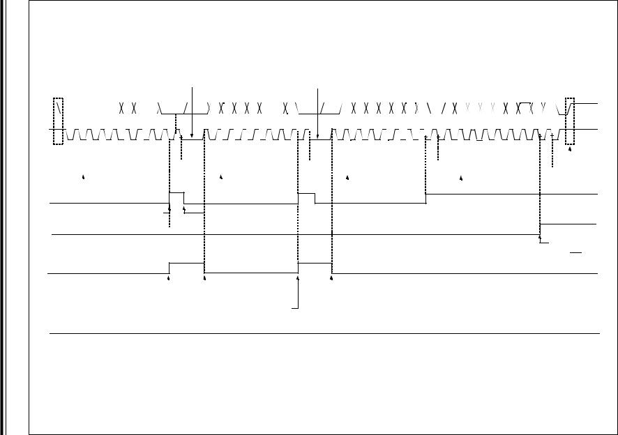
19.4.3.2Address Masking
Masking an address bit causes that bit to become a “don’t care”. When one address bit is masked, two addresses will be Acknowledged and cause an interrupt. It is possible to mask more than one address bit at a time, which makes it possible to Acknowledge up to 31 addresses in 7-bit mode and up to 63 addresses in 10-bit mode (see Example 19-2).
The I2C Slave behaves the same way whether address masking is used or not. However, when address masking is used, the I2C slave can Acknowledge multiple addresses and cause interrupts. When this occurs, it is necessary to determine which address caused the interrupt by checking SSPBUF.
In 7-Bit Address mode, address mask bits ADMSK<5:1> (SSPCON2<5:1>) mask the corresponding address bits in the SSPADD register. For any ADMSK bits that are set (ADMSK<n> = 1), the corresponding address bit is ignored (SSPADD<n> = x). For the module to issue an address Acknowledge, it is sufficient to match only on addresses that do not have an active address mask.
In 10-Bit Address mode, bits ADMSK<5:2> mask the corresponding address bits in the SSPADD register. In addition, ADMSK1 simultaneously masks the two LSbs of the address (SSPADD<1:0>). For any ADMSK bits that are active (ADMSK<n> = 1), the corresponding address bit is ignored (SSPADD<n> = x). Also note that although in 10-Bit Addressing mode, the upper address bits reuse part of the SSPADD register bits, the address mask bits do not interact with those bits. They only affect the lower address bits.
Note 1: ADMSK1 masks the two Least Significant bits of the address.
2:The two Most Significant bits of the address are not affected by address masking.
EXAMPLE 19-2: ADDRESS MASKING EXAMPLES
7-bit addressing:
SSPADD<7:1> = A0h (1010000) (SSPADD<0> is assumed to be ‘0’)
ADMSK<5:1> = 00111
Addresses Acknowledged : A0h, A2h, A4h, A6h, A8h, AAh, ACh, AEh
10-bit addressing:
SSPADD<7:0> = A0h (10100000) (The two MSbs of the address are ignored in this example, since they are not affected by masking)
ADMSK<5:1> = 00111
Addresses Acknowledged: A0h, A1h, A2h, A3h, A4h, A5h, A6h, A7h, A8h, A9h, AAh, ABh, ACh, ADh, AEh, AFh
DS39632D-page 208 |
Preliminary |
♥ 2007 Microchip Technology Inc. |
PIC18F2455/2550/4455/4550
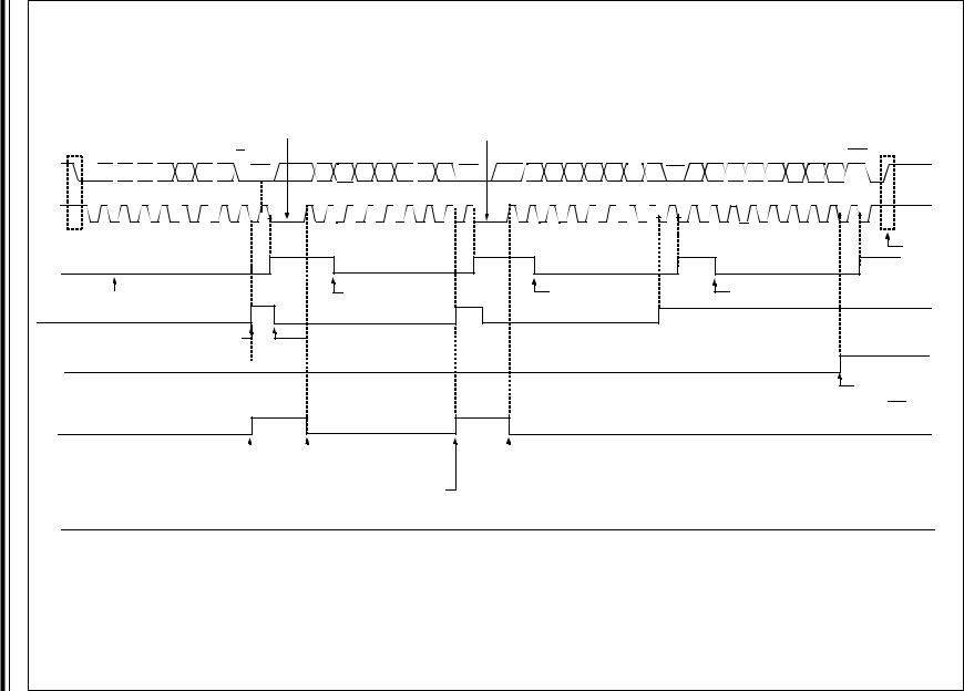
19.4.3.3Reception
When the R/W bit of the address byte is clear and an address match occurs, the R/W bit of the SSPSTAT register is cleared. The received address is loaded into the SSPBUF register and the SDA line is held low (ACK).
When the address byte overflow condition exists, then the no Acknowledge (ACK) pulse is given. An overflow condition is defined as either bit BF (SSPSTAT<0>) is set, or bit SSPOV (SSPCON1<6>) is set.
An MSSP interrupt is generated for each data transfer byte. The Interrupt Flag bit, SSPIF, must be cleared in software. The SSPSTAT register is used to determine the status of the byte.
If SEN is enabled (SSPCON2<0> = 1), RB1/AN10/ INT1/SCK/SCL will be held low (clock stretch) following each data transfer. The clock must be released by setting bit, CKP (SSPCON1<4>). See Section 19.4.4 “Clock Stretching” for more detail.
19.4.3.4Transmission
When the R/W bit of the incoming address byte is set and an address match occurs, the R/W bit of the SSPSTAT register is set. The received address is loaded into the SSPBUF register. The ACK pulse will be sent on the ninth bit and pin RB1/AN10/INT1/SCK/ SCL is held low regardless of SEN (see Section 19.4.4 “Clock Stretching” for more detail). By stretching the clock, the master will be unable to assert another clock pulse until the slave is done preparing the transmit data. The transmit data must be loaded into the SSPBUF register which also loads the SSPSR register. Then pin RB1/AN10/INT1/SCK/SCL should be enabled by setting bit, CKP (SSPCON1<4>). The eight data bits are shifted out on the falling edge of the SCL input. This ensures that the SDA signal is valid during the SCL high time (Figure 19-10).
The ACK pulse from the master-receiver is latched on the rising edge of the ninth SCL input pulse. If the SDA line is high (not ACK), then the data transfer is complete. In this case, when the ACK is latched by the slave, the slave logic is reset (resets SSPSTAT register) and the slave monitors for another occurrence of the Start bit. If the SDA line was low (ACK), the next transmit data must be loaded into the SSPBUF register. Again, pin RB1/AN10/INT1/SCK/SCL must be enabled by setting bit CKP (SSPCON1<4>).
An MSSP interrupt is generated for each data transfer byte. The SSPIF bit must be cleared in software and the SSPSTAT register is used to determine the status of the byte. The SSPIF bit is set on the falling edge of the ninth clock pulse.
♥ 2007 Microchip Technology Inc.
Preliminary
DS39632D-page 209
210 page-DS39632D
Preliminary
.Inc Technology Microchip 2007 ♥
|
|
|
|
|
|
|
|
|
|
|
|
|
|
|
|
|
|
|
|
|
|
|
|
|
|
|
|
|
|
|
|
|
|
|
|
|
|
|
|
|
|
|
|
|
|
|
|
|
|
|
|
|
|
|
|
|
|
|
|
|
|
|
|
|
|
|
|
|
Receiving Address |
R/W = 0 |
|
|
|
|
Receiving Data |
|
|
|
|
|
|
|
|
ACK |
|
|
|
Receiving Data |
|
|
|
|
|
|
ACK |
|
|||||||||||||||||||||||||
|
|
|
|
|
|
|
|
|
|
|
|
|
|
|
|
|
|
|
|
|
|
|
|
|
|
|
|
|
|
|
|
|
|
|
|
|
|
|
|
|
|
|
|
|
|
|
|
|
|
|
|
|
|
|
|
|
|
|
|
|
SDA |
|
|
|
A7 A6 A5 A4 A3 A2 A1 |
|
|
|
|
|
|
|
|
|
|
|
|
|
|
|
|
|
|
|
|
|
|
|
|
|
|
|
|
|
|
|
|
|
|
|
|
|
|
|
|
|
|
|
|
||||||||||||
|
|
|
|
|
|
|
ACK |
|
D7 D6 D5 D4 D3 |
|
D2 D1 D0 |
|
|
D7 |
|
D6 D5 D4 D3 D2 |
|
D1 D0 |
|
|||||||||||||||||||||||||||||||||||||||||
|
|
|
|
|
|
|
|
|
|
|
|
|
|
|
|
|
|
|
|
|
|
|
|
|
|
|
|
|
|
|
|
|
|
|
|
|
|
|
|
|
|
|
|
|
|
|
|
|
|
|
|
|
|
|
|
|
|
|
|
|
SCL |
1 |
2 |
3 |
4 |
5 |
6 |
7 |
8 |
9 |
1 |
2 |
3 |
4 |
5 |
6 |
7 |
8 |
9 |
1 |
2 |
3 |
4 |
5 |
6 |
7 |
8 |
9 |
P |
S |
|
|
|
|
|
|
|
|
|
|
|
|
|
|
|
|
|
|
|
|
|
|
|
|
|
|
|
SSPIF (PIR1<3>)
Bus master terminates transfer
BF (SSPSTAT<0>)
Cleared in software
SSPBUF is read
SSPOV (SSPCON1<6>)
SSPOV is set because SSPBUF is
still full. ACK is not sent.
CKP |
(CKP does not reset to ‘0’ when SEN = 0) |
8:-19 FIGURE |
|
PIC18F2455/2550/4455/4550 |
0=SENWITHTIMINGMODE SLAVE C™ |
|
|
I |
|
|
2 |
|
|
ADDRESS) BIT-7 (RECEPTION, |
|
|
|
|
|
.Inc Technology Microchip 2007 ♥
Preliminary
211 page-DS39632D
|
|
|
|
|
|
|
|
|
|
|
|
|
|
|
|
|
|
|
|
|
|
|
|
|
|
|
|
|
|
|
|
|
|
|
|
|
|
|
|
|
|
|
|
|
|
|
|
|
|
|
|
|
|
|
|
|
|
|
|
|
|
|
|
|
|
|
|
|
|
Receiving Address |
|
|
|
R/W = 0 |
|
|
|
|
Receiving Data |
|
|
|
|
|
|
|
|
ACK |
|
Receiving Data |
|
|
|
|
|
|
ACK |
|
|||||||||||||||||||||||||
SDA |
|
|
|
|
|
|
|
|
|
|
|
|
|
|
|
|
|
|
|
|
|
|
|
|
|
|
|
|
|
|
|
|
|
|
|
|
|
|
|
|
|
|
|
|
|
|
|
|
|
|
|
|
|
|
|
|
|
|
|
|
|
|
|
|
|
|
|
|
|
|
|
|
|
|
|
|
|
|
|
|
|
|
|
|
|
|
|
|
|
|
|
|
|
|
|
|
|
|
|
|
|
|
|
|
|
|
|
|
|
|
|
|
|
|
|
|
|
|
|
|
|
|
|
|
|
|
A7 A6 A5 |
|
X |
|
A3 |
X |
|
X |
|
|
|
|
ACK |
|
D7 D6 D5 D4 D3 |
|
D2 D1 D0 |
|
|
D7 D6 |
|
D5 D4 D3 D2 |
|
D1 D0 |
|
||||||||||||||||||||||||||||||||||
|
|
|
|
|
|
|
|
|
|
|
|
|
|
|
|
|
|
|
|
|
|
|
|
|
|
|
|
|
|
|
|
|
|
|
|
|
|
|
|
|
|
|
|
|
|
|
|
|
|
|
|
|
|
|
|
|
|
|
|
|
|
SCL |
1 |
2 |
3 |
4 |
5 |
6 |
7 |
8 |
9 |
1 |
2 |
3 |
4 |
5 |
6 |
7 |
8 |
9 |
1 |
2 |
3 |
4 |
5 |
6 |
7 |
8 |
9 |
P |
S |
|
|
|
|
|
|
|
|
|
|
|
|
|
|
|
|
|
|
|
|
|
|
|
|
|
|
|
SSPIF (PIR1<3>)
Bus master terminates transfer
BF (SSPSTAT<0>)
Cleared in software
SSPBUF is read
SSPOV (SSPCON1<6>)
SSPOV is set because SSPBUF is
still full. ACK is not sent.
CKP
(CKP does not reset to ‘0’ when SEN = 0)
Note 1: x = Don’t care (i.e., address bit can be either a ‘1’ or a ‘0’).
2:In this example, an address equal to A7.A6.A5.X.A3.X.X will be Acknowledged and cause an interrupt.
|
9:-19 FIGURE |
|
|
ADDRESS) BIT-7 (RECEPTION, |
I |
|
PIC18F2455/2550/4455/4550 |
010110=ADMSK<5:1>AND=SENWITH TIMING MODE SLAVE C™ |
|
||
|
2 |
|
|
|
|
|
|
212 page-DS39632D
Preliminary
.Inc Technology Microchip 2007 ♥
|
|
|
|
|
|
|
|
|
|
|
|
|
|
|
|
|
|
|
|
|
|
|
|
|
|
|
|
|
|
|
|
|
|
|
|
|
|
|
|
|
|
|
|
|
|
|
|
|
|
|
|
|
|
|
|
|
|
|
Transmitting Data |
|
|
|
|
|
|
|
|
|
|
|
|
|
|||||||||||
|
|
|
|
|
|
|
|
|
|
|
|
|
|
Receiving Address |
|
|
|
R/W = 1 |
|
|
|
|
|
|
|
|
|
|
|
|
|
|
|
|
|
|
|
|
|
|
|
|
|
|
|
|
|
|
|
|
|
||||||||||||||||||||||||||||||||
|
|
|
|
|
|
|
|
|
|
|
|
|
|
|
|
|
|
|
|
|
|
|
|
|
|
|
|
|
|
|
|
|
|
|
|
|
|
|
|
|
|
|
|
|
ACK |
||||||||||||||||||||||||||||||||||||||
|
|
|
|
|
|
|
|
|
|
|
|
|
|
|
|
|
|
|
|
|
|
|
|
|
|
|
|
|
|
|
|
|
|
|
|
|
|
|
|
|
|
|
|
|
|
|
|
|
|
|
|
|
|
|
|
|
|
|
|
|
|
|
|
|
|
|
|
|
|
|
|
|
|
|
|
|
|
|
|
||||
SDA |
|
|
|
A7 |
|
A6 |
|
|
|
A4 |
|
A3 |
|
|
|
|
|
|
|
|
|
|
|
|
|
|
|
|
|
D7 |
|
D6 |
|
|
|
|
|
|
|
|
|
|
|
|
|
|
|
|
|
|
|||||||||||||||||||||||||||||||||
|
|
|
|
|
A5 |
|
|
A2 |
A1 |
|
|
|
|
|
|
|
ACK |
|
|
|
|
D5 |
|
D4 |
|
D3 |
|
D2 |
D1 |
|
D0 |
|
|
|
|
||||||||||||||||||||||||||||||||||||||||||||||||
SCL |
|
|
|
|
|
|
|
|
|
|
|
|
|
|
|
|
|
|
|
|
|
|
|
|
|
|
|
|
|
|
|
|
|
|
|
|
|
|
|
|
|
|
|
|
|
|
|
|
|
|
|
|
|
|
|
|
|
|
|
|
|
|
|
|
|
|
|
|
|
|
|
|
|
|
|
|
|
|
|
|
|
|
|
|
|
|
|
|
|
|
|
|
|
|
|
|
|
|
|
|
|
|
|
|
|
|
|
|
|
|
|
|
|
|
|
|
|
|
|
|
|
|
|
|
|
|
|
|
|
|
|
|
|
|
|
|
|
|
|
|
|
|
|
|
|
|
|
|
|
|
|
|
|
|
|
|
|
|
|
|
|
|
|
|
|
|
|
|
|
|
|
|
|
|
|
|
|
|
|
|
|
|
|
|
|
|
|
|
|
|
|
|
|
|
|
|
|
|
|
|
|
|
|
|
|
|
|
|
|
|
|
|
|
|
|
|
|
|
|
|
|
|
|
|
|
|
|
|
|
|
|
|
|
|
|
|
|
|
|
|
|
|
|
|
|
|
|
|
|
|
|
1 |
|
|
2 |
|
3 |
|
4 |
|
5 |
|
|
|
6 |
|
|
|
7 |
|
|
8 |
|
|
|
9 |
|
|
|
|
|
|
1 |
|
|
2 |
|
3 |
|
4 |
|
5 |
|
6 |
|
|
7 |
|
8 |
|
|
|
9 |
|
|
|
|||||||||||||||||||||||||||||
|
S |
|
|
|
|
|
|
|
|
|
|
|
|
|
|
|
|
|
|
|
|
|
|
|
|
|
|
|
|
|
|
|
|
|
|
|
|
|
|
|
|
|
|
|
|
|
|
|
|
|
|
|
|
|
|
|
|
|
|
|
|
|
|
|
|
|
|
|
|
|
|
|
|
|
|
|
|
|
|
|
|
|
|
 Data in
 sampled
SSPIF (PIR1<3>)
BF (SSPSTAT<0>)
 SCL held low
  while CPU
  responds to SSPIF
Cleared in software
 From SSPIF
 ISR
ISR
SSPBUF is written in software
CKP
CKP is set in software
|
|
|
|
|
|
|
|
|
|
|
|
|
|
|
Transmitting Data |
|
|
|
|
|
|
|
|
|
|
|
|
|
|
|
||||||||||||
|
|
|
|
|
|
|
|
|
|
|
|
|
|
|
|
|
|
|
|
ACK |
|
|
|
|
|
|||||||||||||||||
|
|
|
|
|
|
|
|
|
|
|
|
|
|
|
|
|
|
|
|
|
|
|
|
|
|
|
|
|
|
|
|
|
|
|
|
|
|
|||||
D7 |
|
D6 |
|
D5 |
|
D4 |
|
D3 |
|
D2 |
|
D1 |
D0 |
|
|
|
|
|
|
|
|
|
|
|
|
|||||||||||||||||
|
|
|
|
|
|
|
|
|
|
|
|
|
|
|
|
|
|
|
|
|
|
|
|
|
|
|
|
|
|
|
|
|
|
|
|
|
|
|
|
|
|
|
|
|
|
|
|
|
|
|
|
|
|
|
|
|
|
|
|
|
|
|
|
|
|
|
|
|
|
|
|
|
|
|
|
|
|
|
|
|
|
|
|
|
|
1 |
|
2 |
|
3 |
|
4 |
|
5 |
|
6 |
|
7 |
|
|
8 |
|
9 |
|
|
|
|
|
|
|
|
|
||||||||||||||||
|
|
|
|
|
|
|
|
|
|
|
|
|
|
|
|
|
|
|
|
|
|
|
|
|
|
|
|
|
|
|
|
|
|
|
|
|
|
|
|
|
|
|
P
Cleared in software
 From SSPIF ISR
SSPBUF is written in software
CKP is set in software
10:-19 FIGURE |
|
PIC18F2455/2550/4455/4550 |
(TRANSMISSION,TIMINGMODE SLAVE C™ |
|
|
I |
|
|
2 |
|
|
BIT-7 |
|
|
ADDRESS) |
|
|
|
|
|
.Inc Technology Microchip 2007 ♥
Preliminary
213 page-DS39632D
|
|
|
|
|
|
|
|
|
|
|
|
|
|
|
|
|
|
|
|
|
Clock is held low until |
|
Clock is held low until |
|
|
|
|
|
|
|
|
|
|
|
|
|
|
|
|
|
|
|
|
|
|
|
|
|
|||||||||||||||||||||||||||||
|
|
|
|
|
|
|
|
|
|
|
|
|
|
|
|
|
|
|
|
|
update of SSPADD has |
|
update of SSPADD has |
|
|
|
|
|
|
|
|
|
|
|
|
|
|
|
|
|
|
|
|
|
|
|
|
|
|||||||||||||||||||||||||||||
|
|
|
|
|
|
|
|
|
|
|
|
|
|
|
|
|
|
|
|
|
taken place |
|
taken place |
|
|
|
|
|
|
|
|
|
|
|
|
|
|
|
|
|
|
|
|
|
|
|
|
|
|
|
|
|
|
|
|
|
|
|
|
||||||||||||||||||
|
|
|
|
Receive First Byte of Address |
|
|
|
|
Receive Second Byte of Address |
|
|
|
|
|
|
|
|
|
|
Receive Data Byte |
|
|
|
|
|
|
|
|
|
Receive Data Byte |
|
|
|
||||||||||||||||||||||||||||||||||||||||||||
|
|
|
|
|
|
|
|
|
|
|
|
|
|
|
|
R/W = 0 |
|
|
|
|
|
|
|
|
|
|
|
|
|
|
|
|
|
|
|
|
|
|
|
|
|
|
|
|
|
|
|
|
|
|
|
|
|
|
|
|
|
|
|
|
|
|
|
|
|
|
|
|
|
|
|
ACK |
|||||
|
|
|
|
|
|
|
|
|
|
|
|
|
|
|
|
|
|
|
|
|
|
|
|
|
|
|
|
|
|
|
|
|
|
|
|
|
|
|
|
|
|
|
|
|
|
|
|
|
|
|
|
|
|
|
|
|
|
|
|
|
|
|
|
|
|
|
|
|
|
|
|
|
|
|
|
|
|
SDA |
|
|
1 1 1 1 0 A9 A8 |
|
|
ACK |
|
A7 A6 A5 A4 A3 A2 A1 |
A0 ACK |
D7 D6 D5 D4 D3 D2 |
|
D1 D0 ACK D7 D6 D5 D4 D3 D2 D1 D0 |
|
|
|
||||||||||||||||||||||||||||||||||||||||||||||||||||||||||||||
|
|
|
|
|
|
|
|
|
|
|
|
|
|
|
|
|
|
|
|
|
|
|
|
|
|
|
|
|
|
|
|
|
|
|
|
|
|
|
|
|
|
|
|
|
|
|
|
|
|
|
|
|
|
|
|
|
|
|
|
|
|
|
|
|
|
|
|
|
|
|
|
|
|
|
|
|
|
SCL |
S |
1 |
2 |
3 |
4 |
5 |
6 |
7 |
8 |
9 |
1 |
2 |
3 |
4 |
5 |
6 |
7 |
8 |
9 |
1 |
2 |
3 |
4 |
5 |
6 |
7 |
8 |
9 |
1 |
2 |
3 |
4 |
5 |
6 |
7 |
8 |
9 |
P |
|
|
|
|
|
|
|
|
|
|
|
|
|
|
|
|
|
|
|
|
|
|
|
|
|
|
|
|
|
|
|
|
|
|
|
|
|
|
|
|
|
|
|
|
|
|
|
|
|
|
|
|
Bus master |
|
|
|
|
|
|
|
|
|
|
|
|
|
|
|
|
SSPIF (PIR1<3>) |
|
|
|
|
|
|
|
|
|
|
|
|
terminates |
||
|
|
|
|
|
|
|
|
|
|
|
|
transfer |
|||
|
|
|
|
|
|
|
|
|
|
|
|
|
|
|
|
|
|
|
|
|
Cleared in software |
|
|
Cleared in software |
|
|
Cleared in software |
||||
|
|
|
|
|
|
|
|
|
|||||||
|
|
Cleared in software |
|
|
|
||||||||||
|
|
|
|
|
|
|
|
||||||||
|
|
|
|
|
|
|
|
|
|
|
|
|
|
|
|
BF (SSPSTAT<0>)
SSPBUF is written with |
Dummy read of SSPBUF |
contents of SSPSR |
to clear BF flag |
SSPOV (SSPCON1<6>)
UA (SSPSTAT<1>)
UA is set indicating that  the SSPADD needs to be updated
 Cleared by hardware when SSPADD is updated with low byte of address
UA is set indicating that SSPADD needs to be updated
SSPOV is set because SSPBUF is
still full. ACK is not sent.
 Cleared by hardware when SSPADD is updated with high byte of address
CKP |
(CKP does not reset to ‘0’ when SEN = 0) |
11:-19 FIGURE |
|
|
I |
|
|
2 |
|
|
ADDRESS) BIT-10 (RECEPTION, 0 = SEN WITH TIMING MODE SLAVE C™ |
|
PIC18F2455/2550/4455/4550 |
214 page-DS39632D
Preliminary
.Inc Technology Microchip 2007 ♥
Clock is held low until |
Clock is held low until |
update of SSPADD has |
update of SSPADD has |
taken place |
taken place |
|
|
Receive First Byte of Address |
R/W = 0 |
Receive Second Byte of Address |
|
|
|
|
Receive Data Byte |
|
|
|
|
Receive Data Byte |
|
|
ACK |
|
||||||||||||||||||||
|
|
|
|
|
|
|
|
|
|
|
|
|
|
|
|
|
|
|
|
|
|
|
|
|
|
|
|
|
|
|
|
|
|
|
||||
SDA |
|
1 |
1 |
1 |
1 |
0 |
A9 |
A8 |
|
ACK |
A7 |
A6 |
A5 |
X |
A3 |
A2 |
X |
X |
ACK |
D7 |
D6 |
D5 |
D4 |
D3 |
D2 |
D1 |
D0 ACK D7 |
D6 |
D5 |
D4 |
D3 |
D2 |
D1 |
D0 |
|
|
||
SCL |
S |
1 |
2 |
3 |
4 |
5 |
6 |
7 |
8 |
9 |
1 |
2 |
3 |
4 |
5 |
6 |
7 |
8 |
9 |
1 |
2 |
3 |
4 |
5 |
6 |
7 |
8 |
9 |
1 |
2 |
3 |
4 |
5 |
6 |
7 |
8 |
9 |
P |
|
|
|
|
|
|
|
|
|
|
|
|
|
|
|
|
|
|
|
|
|
|
|
|
|
|
|
|
|
|
|
|
|
|
|
|
|
||
|
|
|
|
|
|
|
|
|
|
|
|
|
|
|
|
|
|
|
|
|
|
|
|
|
|
|
|
|
|
|
|
|
|
|
|
|
|
Bus master |
SSPIF (PIR1<3>) |
|
|
|
|
|
|
|
|
|
|
|
|
|
|
|
|
|
|
|
|
|
|
|
|
|
|
|
|
|
|
|
|
|
|
|
terminates |
||
|
|
|
|
|
|
|
|
|
|
|
|
|
|
|
|
|
|
|
|
|
|
|
|
|
|
|
|
|
|
|
|
|
|
|
transfer |
|||
|
|
|
|
|
|
|
|
|
|
|
|
|
|
|
|
|
|
|
|
|
|
|
|
|
|
|
|
|
|
|
|
|
|
|
|
|
|
|
|
|
|
Cleared in software |
|
|
|
|
|
|
Cleared in software |
|
|
|
|
Cleared in software |
|
|
|
|
|
Cleared in software |
|
|
|
|
|||||||||||||
|
|
|
|
|
|
|
|
|
|
|
|
|
|
|
|
|
|
|
|
|
|
|
|
|
|
|
|
|
|
|
|
|
|
|
||||
BF (SSPSTAT<0>)
SSPBUF is written with |
Dummy read of SSPBUF |
contents of SSPSR |
to clear BF flag |
SSPOV (SSPCON1<6>)
SSPOV is set because SSPBUF is
still full. ACK is not sent.
UA (SSPSTAT<1>)
UA is set indicating that  the SSPADD needs to be updated
 Cleared by hardware when SSPADD is updated with low byte of address
UA is set indicating that SSPADD needs to be updated
 Cleared by hardware when SSPADD is updated with high byte of address
CKP
(CKP does not reset to ‘0’ when SEN = 0)
Note 1: x = Don’t care (i.e., address bit can be either a ‘1’ or a ‘0’).
2:In this example, an address equal to A9.A8.A7.A6.A5.X.A3.A2.X.X will be Acknowledged and cause an interrupt.
3:Note that the Most Significant bits of the address are not affected by the bit masking.
12:-19 FIGURE |
|
PIC18F2455/2550/4455/4550 |
0=SENWITHTIMINGMODE SLAVE C™ ADDRESS)BIT-10 (RECEPTION, |
|
|
I |
|
|
2 |
|
|
01001 = ADMSK<5:1> AND |
|
|
|
|
|
.Inc Technology Microchip 2007 ♥
Preliminary
215 page-DS39632D
|
|
Bus master |
Clock is held low until |
Clock is held low until |
terminates |
transfer |
|
|
|
|
|
|
|
|
|
|
|
|
|
|
|
|
|
|
|
|
|
update of SSPADD has |
|
update of SSPADD has |
|
|
|
|
Clock is held low until |
|
|
|
|
|
|||||||||||||||||||||||||||||||||||||||||||||||
|
|
|
|
|
|
|
|
|
|
|
|
|
|
|
|
|
|
|
|
|
taken place |
|
taken place |
|
|
|
|
|
|
|
|
|
|
|
|
|
|
|
|
|
CKP is set to ‘1’ |
|
|
|
|
|
||||||||||||||||||||||||||||||||||
|
|
|
|
Receive First Byte of Address |
|
|
|
|
|
|
|
|
|
|
|
|
|
|
|
|
|
|
|
|
|
|
|
|
|
|
|
|
|
|
|
|
|
|
|
|
|
|
|
|
|
|
|
|
|
|
|
|
|
|
|
|
|
|
|
|
|
|
|
|
|
|
|
|
||||||||||||
|
|
|
|
R/W |
= 0 |
|
Receive Second Byte of Address |
|
|
|
|
|
|
|
Receive First Byte of Address |
R/W |
= 1 |
|
|
|
Transmitting Data Byte |
|
|
|
ACK |
|||||||||||||||||||||||||||||||||||||||||||||||||||||||
|
|
|
|
|
|
|
|
|
|
|
|
|
|
|
|
|
|
|
|
|
|
|
|
|
|
|
|
|
|
|
|
|
|
|
|
|
|
|
|
|
|
|
|
|
|
|
|
|
|
|
|
|
|
|
|
|
|
|
|
|
|
|
|
|
|
|
|
|
|
|
|
|
|
|
|
|
|
|||
SDA |
|
|
|
|
|
|
|
|
|
|
|
|
|
|
|
|
|
|
|
|
A7 A6 A5 A4 A3 A2 A1 A0 |
|
|
|
|
|
|
|
1 1 1 1 0 A9 A8 |
|
|
|
|
|
|
D7 D6 D5 D4 D3 D2 D1 |
|
D0 |
||||||||||||||||||||||||||||||||||||||||||
|
|
1 1 1 1 0 A9 A8 |
|
|
|
|
|
|
ACK |
|
|
|
|
|
|
|
|
ACK |
|
|||||||||||||||||||||||||||||||||||||||||||||||||||||||||||||
|
|
ACK |
|
|
|
|
|
|
|
|
|
|
||||||||||||||||||||||||||||||||||||||||||||||||||||||||||||||||||||
|
|
|
|
|
|
|
|
|
|
|
|
|
|
|
|
|
|
|
|
|
|
|
|
|
|
|
|
|
|
|
|
|
|
|
|
|
|
|
|
|
|
|
|
|
|
|
|
|
|
|
|
|
|
|
|
|
|
|
|
|
|
|
|
|
|
|
|
|
|
|
|
|
|
|
|
|
|
|
|
|
SCL |
S |
1 |
2 |
3 |
4 |
5 |
6 |
7 |
8 |
9 |
1 |
2 |
3 |
4 |
5 |
6 |
7 |
8 |
9 |
1 |
2 |
3 |
4 |
5 |
6 |
7 |
8 |
9 |
1 |
2 |
3 |
4 |
5 |
6 |
7 |
8 |
9 |
P |
|
|
|
|
|
|
|
|
|
|
|
|
|
|
|
|
|
|
|
Sr |
|
|
|
|
|
|
|
|
|
|
|
|
|
|
|
|
|
||
|
|
|
|
|
|
|
|
|
|
|
|
|
|
|
|
|
|
|
|
|
|
|
|
|
|
|
|
|
|
|
|
|
|
|
|
|
|
SSPIF (PIR1<3>)
Cleared in software |
Cleared in software |
Cleared in software |
BF (SSPSTAT<0>)
SSPBUF is written with  contents of SSPSR
UA (SSPSTAT<1>)
UA is set indicating that  the SSPADD needs to be updated
CKP (SSPCON1<4>)
 Dummy read of SSPBUF to clear BF flag
 Cleared by hardware when SSPADD is updated with low byte of address
UA is set indicating that SSPADD needs to be updated
|
|
|
Dummy read of SSPBUF |
|
|
|
|
|
|
|
|
|
|
|
BF flag is clear |
|
|
Write of SSPBUF |
Completion of |
||||
|
|
|
to clear BF flag |
|
|
||||||
|
|
|
at the end of the |
|
|
initiates transmit |
data transmission |
||||
|
|
|
|
|
|
|
|||||
|
|
|
|
|
third address sequence |
clears BF flag |
|||||
|
|
|
|
|
|
|
|
|
|
|
|
 Cleared by hardware when SSPADD is updated with high byte of address.
 CKP is set in software
CKP is automatically cleared in hardware, holding SCL low
13:-19 FIGURE |
|
|
I |
|
|
2 |
|
|
ADDRESS) BIT-10 (TRANSMISSION, TIMING MODE SLAVE C™ |
|
PIC18F2455/2550/4455/4550 |