

Архив4 / Proshin_polnostyu_ves_kursach / EPM570Z
.pdf
|
|
Dedicated Pin Information for the MAX® IIZ |
|
|
|
|
EPM570Z Devices |
|
|
|
Version 1.0 |
|
|
|
|
Dedicated Pin |
100-Pin MBGA |
144-Pin MBGA |
256-Pin MBGA |
IO/GCLK0 |
F2 |
A8 |
K1 |
IO/GCLK1 |
E1 |
B6 |
L1 |
IO/GCLK2 |
F10 |
N7 |
M20 |
IO/GCLK3 |
G11 |
N8 |
L20 |
IO/DEV_OE |
L8 |
J4 |
W12 |
IO/DEV_CLRn |
K8 |
K1 |
Y13 |
TDI |
J2 |
A3 |
U2 |
TMS |
J1 |
B3 |
T3 |
TCK |
K1 |
A1 |
W2 |
TDO |
K2 |
A2 |
V2 |
|
|
C6, C7, C8, F3. F11, G3, G11, H3, H11, |
J4, U12, M17, D12, H3, J3, M4, N3, U9, |
|
|
V8, V9, V13, H18, J17, N18, C8, D9, C12, |
|
GND(3) |
E4, G4, H5, J5. H7. G8, E8, D7, C5, D5 |
L6, L7, L8 |
C13, M18 |
VCCINT (1) |
G3, J7, E9, C7 |
D7, G4, G10, K7 |
K4, U11, L17, D11 |
VCCIO1 (2) |
E3, J4, J8 |
D6, D8, F4, H4 |
K3, L3, L4, M3, U10, V10, V11, V12 |
VCCIO2 (2) |
G9, C8, C4 |
F10, J10, K6, K8 |
J18, K17, K18, L18, C9, C10, D10, C11 |
|
|
|
D5, C7, D8, D14, C14, C4, D6, C6, B10, |
|
|
|
B11, D16, D15, F18, D4, H4, G4, D7, |
|
|
|
D13, G17, D17, E4, G3, F4, H17, G18, |
|
|
|
F17, K2, K19, L2, L19, R4, P4, N4, N17, |
|
|
|
P18, R17, P3, U8, U16, T17, P17, U6, U7, |
|
|
|
U13, U14, U15, U5, V7, W9, W10, V15, |
No Connect (N.C.) |
- |
- |
V14, |
Total User I/O Pins |
76 |
116 |
160 |
Notes:
(1)All VCCINT pins must be connected to 1.8 V.
(2)Each set of VCCIO pins (VCCIO1 or VCCIO2) can be connected to 3.3 V, 2.5 V, 1.8 V, or 1.5 V.
(3)MAXII and MAXIIG devices separate out I/O ground (GNDIO) and core ground (GNDINT), but MAXII Z devices unify ground to GND only.
PT-EPM570Z-1.0 |
EPM570Z Dedicated |
Page 1 of 9 |
Copyright © 2008 Altera Corp. |

|
|
|
|
|
I/O Pin Information for the MAX® IIZ |
|
|
|
|
|
|
|
EPM570Z Devices |
|
|
|
|
|
|
Version 1.0 |
|
|
|
|
|
|
|
Bank |
Pad Number |
Pin/Pad |
Optional |
100-Pin MBGA |
144-Pin MBGA |
256-Pin MBGA |
Number |
Orientation |
Function |
Function(s) |
|
|
|
B1 |
1 |
VCCIO1 |
|
|
|
|
B1 |
2 |
GND |
|
|
|
|
B1 |
3 |
IO |
|
|
|
D3 |
B1 |
4 |
IO |
|
|
B11 |
C2 |
B1 |
5 |
IO |
|
B1 |
C10 |
E3 |
B1 |
6 |
IO |
|
|
|
C1 |
B1 |
7 |
IO |
|
C2 |
C11 |
D2 |
B1 |
8 |
IO |
|
|
|
D1 |
B1 |
9 |
IO |
|
C1 |
B10 |
C3 |
B1 |
10 |
IO |
|
|
|
F2 |
B1 |
11 |
IO |
|
D3 |
C9 |
H2 |
B1 |
12 |
IO |
|
D2 |
A12 |
E1 |
B1 |
13 |
IO |
|
D1 |
B9 |
B1 |
B1 |
14 |
IO |
|
E2 |
A11 |
G2 |
B1 |
15 |
IO |
|
|
|
F3 |
B1 |
16 |
IO |
|
|
|
E2 |
B1 |
17 |
VCCIO1 |
|
|
|
|
B1 |
18 |
GND |
|
|
|
|
B1 |
19 |
IO |
|
|
D10 |
J2 |
B1 |
20 |
IO |
|
|
A10 |
G1 |
B1 |
21 |
IO |
|
|
B8 |
F1 |
B1 |
22 |
IO |
|
|
B7 |
H1 |
B1 |
23 |
IO |
|
|
D9 |
M2 |
B1 |
24 |
IO |
|
|
A9 |
J1 |
|
25 |
GND |
|
|
|
|
B1 |
26 |
IO |
GCLK0 |
F2 |
A8 |
K1 |
|
27 |
VCCINT |
|
|
|
|
B1 |
28 |
IO |
GCLK1 |
E1 |
B6 |
L1 |
B1 |
29 |
IO |
|
F1 |
C3 |
N2 |
B1 |
30 |
IO |
|
G1 |
A7 |
M1 |
B1 |
31 |
IO |
|
G2 |
C4 |
T4 |
B1 |
32 |
IO |
|
F3 |
A6 |
N1 |
B1 |
33 |
VCCIO1 |
|
|
|
|
B1 |
34 |
GND |
|
|
|
|
B1 |
35 |
IO |
|
|
|
R3 |
B1 |
36 |
IO |
|
|
A5 |
P1 |
B1 |
37 |
IO |
|
|
|
U1 |
B1 |
38 |
IO |
|
|
A4 |
R1 |
B1 |
39 |
IO |
|
|
D5 |
R2 |
B1 |
40 |
IO |
|
|
|
P2 |
B1 |
41 |
IO |
|
H1 |
B5 |
V3 |
B1 |
42 |
IO |
|
|
|
T1 |
B1 |
43 |
IO |
|
H3 |
C5 |
W1 |
B1 |
44 |
IO |
|
|
|
V1 |
B1 |
45 |
IO |
|
H2 |
B4 |
T2 |
B1 |
46 |
IO |
|
|
|
U3 |
B1 |
47 |
TMS |
|
J1 |
B3 |
T3 |
B1 |
48 |
TDI |
|
J2 |
A3 |
U2 |
B1 |
49 |
TCK |
|
K1 |
A1 |
W2 |
B1 |
50 |
TDO |
|
K2 |
A2 |
V2 |
B1 |
51 |
VCCIO1 |
|
|
|
|
B1 |
52 |
GND |
|
|
|
|
B1 |
53 |
NC(1) |
|
|
|
|
B1 |
54 |
IO |
|
|
D2 |
W4 |
B1 |
55 |
IO |
|
|
C2 |
W3 |
B1 |
56 |
IO |
|
|
|
V4 |
B1 |
57 |
IO |
|
|
B2 |
Y1 |
B1 |
58 |
IO |
|
|
|
Y2 |
B1 |
59 |
IO |
|
L1 |
B1 |
W6 |
B1 |
60 |
IO |
|
L2 |
E2 |
W5 |
B1 |
61 |
IO |
|
|
|
Y4 |
B1 |
62 |
IO |
|
K3 |
E3 |
V5 |
B1 |
63 |
IO |
|
L3 |
C1 |
W7 |
B1 |
64 |
IO |
|
K4 |
D3 |
Y3 |
B1 |
65 |
IO |
|
|
|
Y5 |
B1 |
66 |
IO |
|
|
|
U4 |
B1 |
67 |
IO |
|
|
D1 |
Y6 |
B1 |
68 |
VCCIO1 |
|
|
|
|
B1 |
69 |
GND |
|
|
|
|
B1 |
70 |
IO |
|
|
D4 |
V6 |
B1 |
71 |
IO |
|
|
E1 |
Y7 |
B1 |
72 |
IO |
|
L4 |
E4 |
W8 |
B1 |
73 |
IO |
|
K5 |
F1 |
Y8 |
PT-EPM570Z-1.0 |
EPM570Z IO |
Page 2 of 9 |
Copyright © 2008 Altera Corp. |

I/O Pin Information for the MAX® IIZ
EPM570Z Devices
Version 1.0
Bank |
Pad Number |
Pin/Pad |
Optional |
100-Pin MBGA |
144-Pin MBGA |
256-Pin MBGA |
Number |
Orientation |
Function |
Function(s) |
|
|
|
B1 |
74 |
IO |
|
L5 |
F2 |
W11 |
B1 |
75 |
IO |
|
L6 |
G2 |
Y9 |
|
76 |
GND |
|
|
|
|
B1 |
77 |
IO |
|
K6 |
G1 |
Y10 |
|
78 |
VCCINT |
|
|
|
|
B1 |
79 |
IO |
|
J6 |
H1 |
Y11 |
B1 |
80 |
IO |
|
L7 |
H2 |
W14 |
B1 |
81 |
IO |
|
K7 |
J1 |
Y12 |
B1 |
82 |
IO |
DEV_OE |
L8 |
J4 |
W12 |
B1 |
83 |
IO |
DEV_CLRn |
K8 |
K1 |
Y13 |
B1 |
84 |
IO |
|
|
K4 |
W13 |
B1 |
85 |
IO |
|
|
L1 |
Y14 |
B1 |
86 |
VCCIO1 |
|
|
|
|
B1 |
87 |
GND |
|
|
|
|
B1 |
88 |
IO |
|
|
|
W16 |
B1 |
89 |
IO |
|
L9 |
J2 |
Y15 |
B1 |
90 |
IO |
|
K9 |
J3 |
V17 |
B1 |
91 |
IO |
|
L10 |
L2 |
Y16 |
B1 |
92 |
IO |
|
|
|
V16 |
B1 |
93 |
IO |
|
K10 |
K2 |
W15 |
B1 |
94 |
VCCIO1 |
|
|
|
|
B1 |
95 |
GND |
|
|
|
|
B1 |
96 |
IO |
|
|
K3 |
Y18 |
B1 |
97 |
IO |
|
|
|
Y17 |
B1 |
98 |
IO |
|
|
|
V18 |
B1 |
99 |
IO |
|
L11 |
M1 |
W17 |
B1 |
100 |
IO |
|
|
|
Y19 |
B1 |
101 |
IO |
|
|
N1 |
W18 |
B1 |
102 |
VCCIO1 |
|
|
|
|
B1 |
103 |
GND |
|
|
|
|
B2 |
104 |
VCCIO2 |
|
|
|
|
B2 |
105 |
GND |
|
|
|
|
B2 |
106 |
IO |
|
|
L3 |
W19 |
B2 |
107 |
IO |
|
K11 |
M2 |
Y20 |
B2 |
108 |
IO |
|
J10 |
M3 |
V19 |
B2 |
109 |
IO |
|
|
|
T19 |
B2 |
110 |
IO |
|
J11 |
M4 |
U18 |
B2 |
111 |
IO |
|
|
|
V20 |
B2 |
112 |
IO |
|
|
|
U19 |
B2 |
113 |
IO |
|
H9 |
N2 |
R19 |
B2 |
114 |
IO |
|
|
|
R18 |
B2 |
115 |
IO |
|
H10 |
N3 |
U20 |
B2 |
116 |
IO |
|
H11 |
L5 |
T18 |
B2 |
117 |
IO |
|
G10 |
N4 |
T20 |
B2 |
118 |
IO |
|
|
L4 |
U17 |
B2 |
119 |
IO |
|
|
|
P19 |
B2 |
120 |
VCCIO2 |
|
|
|
|
B2 |
121 |
GND |
|
|
|
|
B2 |
122 |
IO |
|
|
M5 |
W20 |
B2 |
123 |
IO |
|
|
N5 |
R20 |
B2 |
124 |
IO |
|
F9 |
M6 |
N19 |
B2 |
125 |
IO |
|
|
N6 |
P20 |
B2 |
126 |
IO |
|
|
M7 |
M19 |
B2 |
127 |
IO |
GCLK2 |
F10 |
N7 |
M20 |
|
128 |
VCCINT |
|
|
|
|
B2 |
129 |
IO |
GCLK3 |
G11 |
N8 |
L20 |
|
130 |
GND |
|
|
|
|
B2 |
131 |
IO |
|
F11 |
N9 |
N20 |
B2 |
132 |
IO |
|
E11 |
K5 |
J19 |
B2 |
133 |
IO |
|
E10 |
N10 |
K20 |
B2 |
134 |
IO |
|
|
M8 |
E17 |
B2 |
135 |
IO |
|
|
N11 |
J20 |
B2 |
136 |
IO |
|
|
K9 |
H19 |
B2 |
137 |
GND |
|
|
|
|
B2 |
138 |
VCCIO2 |
|
|
|
|
B2 |
139 |
IO |
|
|
N12 |
H20 |
B2 |
140 |
IO |
|
|
|
C18 |
B2 |
141 |
IO |
|
D9 |
N13 |
G20 |
B2 |
142 |
IO |
|
D11 |
L9 |
D18 |
B2 |
143 |
IO |
|
|
|
G19 |
B2 |
144 |
IO |
|
|
|
E18 |
B2 |
145 |
IO |
|
D10 |
M12 |
F20 |
B2 |
146 |
IO |
|
C11 |
M9 |
B20 |
PT-EPM570Z-1.0 |
EPM570Z IO |
Page 3 of 9 |
Copyright © 2008 Altera Corp. |

I/O Pin Information for the MAX® IIZ
EPM570Z Devices
Version 1.0
Bank |
Pad Number |
Pin/Pad |
Optional |
100-Pin MBGA |
144-Pin MBGA |
256-Pin MBGA |
Number |
Orientation |
Function |
Function(s) |
|
|
|
B2 |
147 |
IO |
|
|
|
E20 |
B2 |
148 |
IO |
|
C10 |
L10 |
C19 |
B2 |
149 |
IO |
|
|
|
F19 |
B2 |
150 |
IO |
|
B11 |
M10 |
E19 |
B2 |
151 |
IO |
|
|
|
D20 |
B2 |
152 |
IO |
|
B10 |
M11 |
D19 |
B2 |
153 |
IO |
|
|
|
C20 |
B2 |
154 |
NC(1) |
|
|
|
|
B2 |
155 |
VCCIO2 |
|
|
|
|
B2 |
156 |
GND |
|
|
|
|
B2 |
157 |
IO |
|
|
|
A19 |
B2 |
158 |
IO |
|
A11 |
L12 |
A20 |
B2 |
159 |
IO |
|
A10 |
K10 |
C16 |
B2 |
160 |
IO |
|
B9 |
L11 |
B17 |
B2 |
161 |
IO |
|
|
|
A18 |
B2 |
162 |
IO |
|
|
M13 |
A17 |
B2 |
163 |
IO |
|
|
|
B16 |
B2 |
164 |
IO |
|
|
K12 |
B15 |
B2 |
165 |
IO |
|
|
|
C15 |
B2 |
166 |
IO |
|
|
K11 |
B14 |
B2 |
167 |
IO |
|
|
|
B18 |
B2 |
168 |
GND |
|
|
|
|
B2 |
169 |
VCCIO2 |
|
|
|
|
B2 |
170 |
IO |
|
A9 |
L13 |
A16 |
B2 |
171 |
IO |
|
B8 |
J11 |
B19 |
B2 |
172 |
IO |
|
|
K13 |
B13 |
B2 |
173 |
IO |
|
|
J12 |
C17 |
B2 |
174 |
IO |
|
A8 |
J13 |
A15 |
B2 |
175 |
IO |
|
B7 |
H10 |
B12 |
B2 |
176 |
IO |
|
A7 |
H12 |
A14 |
B2 |
177 |
IO |
|
C6 |
E10 |
B9 |
B2 |
178 |
IO |
|
B6 |
H13 |
A13 |
|
179 |
VCCINT |
|
|
|
|
B2 |
180 |
IO |
|
A6 |
G13 |
A12 |
|
181 |
GND |
|
|
|
|
B2 |
182 |
IO |
|
|
G12 |
A11 |
B2 |
183 |
IO |
|
|
D11 |
B8 |
B2 |
184 |
IO |
|
|
F13 |
A10 |
B2 |
185 |
IO |
|
|
F12 |
B2 |
B2 |
186 |
IO |
|
A5 |
E13 |
A9 |
B2 |
187 |
IO |
|
B5 |
E11 |
A5 |
B2 |
188 |
GND |
|
|
|
|
B2 |
189 |
VCCIO2 |
|
|
|
|
B2 |
190 |
IO |
|
A4 |
E12 |
A8 |
B2 |
191 |
IO |
|
B4 |
D12 |
B3 |
B2 |
192 |
IO |
|
A3 |
D13 |
A7 |
B2 |
193 |
IO |
|
|
|
C5 |
B2 |
194 |
IO |
|
B3 |
C13 |
B7 |
B2 |
195 |
IO |
|
A2 |
C12 |
B6 |
B2 |
196 |
IO |
|
|
|
A6 |
B2 |
197 |
IO |
|
B2 |
B12 |
A3 |
B2 |
198 |
GND |
|
|
|
|
B2 |
199 |
VCCIO2 |
|
|
|
|
B2 |
200 |
IO |
|
|
|
A4 |
B2 |
201 |
IO |
|
|
|
B4 |
B2 |
202 |
IO |
|
A1 |
B13 |
B5 |
B2 |
203 |
IO |
|
|
|
A2 |
B2 |
204 |
IO |
|
|
A13 |
A1 |
B2 |
205 |
VCCIO2 |
|
|
|
|
B2 |
206 |
GND |
|
|
|
|
Note:
1. No connect.
PT-EPM570Z-1.0 |
EPM570Z IO |
Page 4 of 9 |
Copyright © 2008 Altera Corp. |

Pin Definitions for the MAX® IIZ
EPM570Z Devices
Version 1.0
Pin Name |
Pin Type |
Pin Description |
|
|
Supply and Reference pins |
|
|
I/O supply voltage pins for banks 1 through 2 respectively. Each VCCIO bank supports a different voltage level with |
|
|
the VCCIO pins providing power for the input and output buffers within that particular I/O bank. Each VCCIO bank |
VCCIO[1..2] |
Power |
can be powered with either 3.3 V, 2.5 V, 1.8 V, or 1.5 V. |
|
|
Device ground pins. Ground pins for all the I/O banks and internal supply. All GND pins should be connected to |
GND(1) |
Ground |
the board GND plane. |
VCCINT |
Power |
Voltage supply pins for the device. |
|
|
Programming and JTAG pins |
|
|
Dual-purpose pin that can override all clears on all device registers. All registers are cleared when the pin is driven |
|
|
low and all registers behave as defined in the design when this pin is driven high. If not used for its dual-purpose |
DEV_CLRn |
I/O |
function, this pin is a regular I/O. |
|
|
Dual-purpose pin that can override all tri-states on the device. All output pins are tristated when the pin is driven |
|
|
low and all output pins behave as defined in the design when this pin is driven high. If not used for its dual-purpose |
DEV_OE |
I/O |
function, this pin is a regular I/O. |
|
||
TCK |
Input |
Dedicated JTAG input pin. |
TDI |
Input |
Dedicated JTAG input pin. |
TMS |
Input |
Dedicated JTAG input pin. |
TDO |
Output |
Dedicated JTAG output pin. |
|
|
Clock Pins |
|
|
Dual-purpose clock pins that connect to the global clock network. If not used for |
GCLK [0..3] |
I/O |
its dual-purpose function, this pin is a regular I/O. |
Note:
1. MAXII and MAXIIG devices separate out I/O ground (GNDIO) and core ground (GNDINT), but MAXII Z devices unify ground to GND only.
PT-EPM570Z-1.0 |
Pin Definitions |
Page 5 of 9 |
Copyright © 2008 Altera Corp. |
Package Diagram and Bank Information for the MAX® IIZ
EPM570Z Devices
Version 1.0
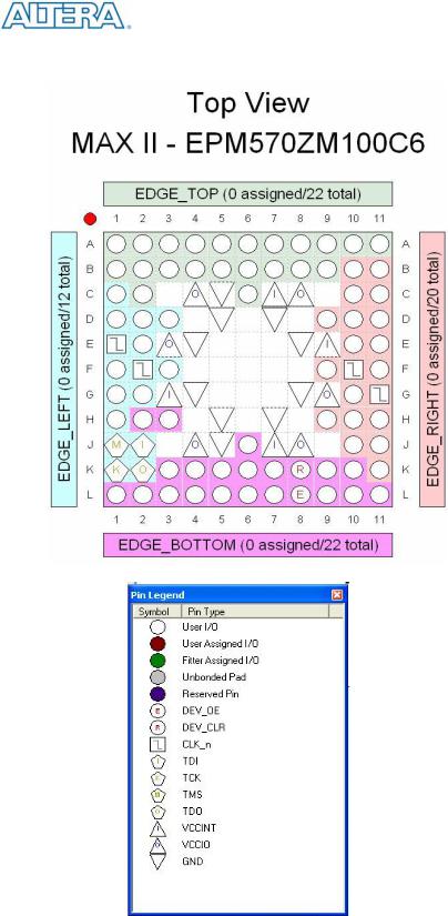
Figure 1. MAX IIZ EPM570Z M100 Device Top View Package Diagram and Bank Information
PT-EPM570Z-1.0 |
EPM570Z M100 |
Page 6 of 9 |
Copyright © 2008 Altera Corp. |

PT-EPM570Z-1.0
Copyright © 2008 Altera Corp.
Package Diagram and Bank Information for the MAX® IIZ
EPM570Z Devices
Version 1.0
Figure 2. MAX IIZ EPM570Z M144 Device Top View Package Diagram and Bank Information
PT-EPM570Z-1.0 |
EPM570Z M144 |
Page 7 of 9 |
Copyright © 2008 Altera Corp. |
Package Diagram and Bank Information for the MAX® IIZ
EPM570Z Devices
Version 1.0
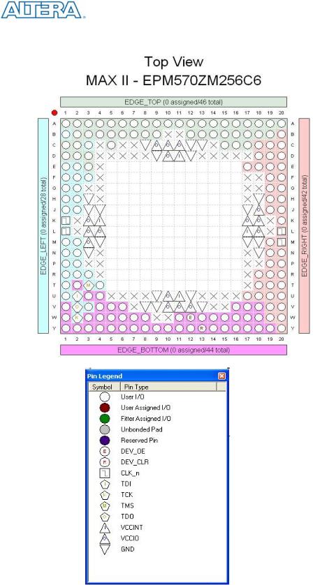
Figure 3. MAX IIZ EPM570Z M256 Device Top View Package Diagram and Bank Information
PT-EPM570Z-1.0 |
EPM570Z M256 |
Page 8 of 9 |
Copyright © 2008 Altera Corp. |

|
|
Revision History for the MAX® IIZ |
|
|
EPM570Z Devices |
|
|
Version 1.0 |
|
|
|
Date |
Version |
Changes Made |
Feb-08 |
1.0 |
Initial release |
|
|
|
|
|
|
|
|
|
|
|
|
PT-EPM570Z-1.0 |
Revision History |
Page 9 of 9 |
Copyright © 2008 Altera Corp. |